 | –≠–ª–µ–∫—Ç—Ä–æ–Ω–Ω—ã–π –∫–æ–º–ø–æ–Ω–µ–Ω—Ç: Le58QL02 | –°–∫–∞—á–∞—Ç—å:  PDF PDF  ZIP ZIP |

TM
Document ID# 080753
Date:
May 24, 2006
Rev:
F
Version: 1
Distribution:
Public Document
Le58QL02/021/031
Quad Low Voltage Subscriber Line Audio-Processing Circuit
VE580 Series
APPLICATIONS
Codec function on telephone switch line cards
FEATURES
Low-power, 3.3 V CMOS technology with 5-V tolerant
digital inputs
Software and coefficient compatible to the Le79Q02/
021/031 QSLACTM device
Performs the functions of four codec/filters
Software programmable:
-- SLIC device input impedance
-- Transhybrid balance
-- Transmit and receive gains
-- Equalization (frequency response)
-- Digital I/O pins
-- Programmable debouncing on one input
-- Time slot assigner
-- Programmable clock slot and PCM transmit clock edge
options
Standard microprocessor interface
A-law, µ-law, or linear coding
Single or Dual PCM ports available
-- Up to 128 channels (PCLK at 8.192 MHz) per PCM port
-- Optional supervision on the PCM highway
1.536, 1.544, 2.048, 3.072, 3.088, 4.096, 6.144, 6.176, or
8.192 MHz master clock derived from MCLK or PCLK
Built-in test modes with loopback, tone generation,
and µP access to PCM data
Mixed state (analog and digital) impedance scaling
Performance guaranteed over a 12 dB gain range
Real Time Data register with interrupt (open drain or
TTL output)
Supports multiplexed SLIC device outputs
Broadcast state
256 kHz or 293 kHz chopper clock for Legerity SLIC
devices with switching regulator
Maximum channel bandwidth for V.90 modems
ORDERING INFORMATION
1.
The green package meets RoHS Directive 2002/95/EC of the
European Council to minimize the environmental impact of
electrical equipment.
2.
For delivery using a tape and reel packing system, add a "T" suffix
to the OPN (Ordering Part Number) when placing an order.
Device
Package (Green)
1
Packing
2
Le58QL02FJC
44-pin PLCC
Tube
Le58QL021FJC
44-pin PLCC
Tube
Le58QL021BVC
44-pin TQFP
Tray
Le58QL031DJC
32-pin PLCC
Tube
RELATED LITERATURE
080754 Le58QL061/063 QLSLACTM Device Data Sheet
080761 QSLACTM to QLSLACTM Device Design
Conversion Guide
080758 QSLACTM to QLSLACTM Guide to New Designs
DESCRIPTION
The Le58QL02/021/031 Quad Low Voltage Subscriber Line
Audio-Processing Circuit (QLSLACTM) devices integrate the
key functions of analog line cards into high-performance, very-
programmable, four-channel codec-filter devices. The
QLSLAC devices are based on the proven design of Legerity's
reliable SLACTM device families. The advanced architecture of
the QLSLAC devices implements four independent channels
and employs digital filters to allow software control of
transmission, thus providing a cost-effective solution for the
audio-processing function of programmable line cards. The
QLSLAC devices are software and coefficient compatible to the
QSLAC devices.
Advanced submicron CMOS technology makes the Le58QL02/
021/031 QLSLAC devices economical, with both the
functionality and the low power consumption needed in line
card designs to maximize line card density at minimum cost.
When used with four Legerity SLIC devices, a QLSLAC device
provides a complete software-configurable solution to the
BORSCHT functions.
BLOCK DIAGRAM
Signal Processing
Channel 1 (CH 1)
Signal Processing
Channel 2 (CH 2)
Signal Processing
Channel 3 (CH 3)
Signal Processing
Channel 4 (CH 4)
VIN
1
VOUT
1
VIN
2
VOUT
2
VIN
3
VOUT
3
VIN
4
VOUT
4
Analog
SLIC
Clock
&
Reference
Circuits
SLIC
Interface
(SLI)
VREF
CD1
1
CD2
1
C3
1
C4
1
C5
1
CD1
2
CD2
2
C3
2
C4
2
C5
2
CD1
3
CD2
3
C3
3
C4
3
C5
3
CD1
4
CD2
4
C3
4
C4
4
C5
4
Time Slot Assigner
(TSA)
DXA
DRA
TSCA
DXB
DRB
TSCB
Microprocessor Interface
(MPI)
INT
CS
DIO
DCLK
RST
FS
PCLK
MCLK/E1
Dual/Single
PCM
Highway
Microprocessor
CHCLK

2
Le58QL02/021/031 VE580 Series Data Sheet
Table of Contents
APPLICATIONS . . . . . . . . . . . . . . . . . . . . . . . . . . . . . . . . . . . . . . . . . . . . . . . . . . . . . . . . . . . . . . . . . . . .1
FEATURES . . . . . . . . . . . . . . . . . . . . . . . . . . . . . . . . . . . . . . . . . . . . . . . . . . . . . . . . . . . . . . . . . . . . . . . .1
ORDERING INFORMATION. . . . . . . . . . . . . . . . . . . . . . . . . . . . . . . . . . . . . . . . . . . . . . . . . . . . . . . . . . .1
RELATED LITERATURE . . . . . . . . . . . . . . . . . . . . . . . . . . . . . . . . . . . . . . . . . . . . . . . . . . . . . . . . . . . . .1
DESCRIPTION . . . . . . . . . . . . . . . . . . . . . . . . . . . . . . . . . . . . . . . . . . . . . . . . . . . . . . . . . . . . . . . . . . . . .1
BLOCK DIAGRAM . . . . . . . . . . . . . . . . . . . . . . . . . . . . . . . . . . . . . . . . . . . . . . . . . . . . . . . . . . . . . . . . . .1
PRODUCT DESCRIPTION . . . . . . . . . . . . . . . . . . . . . . . . . . . . . . . . . . . . . . . . . . . . . . . . . . . . . . . . . . . .5
BLOCK DESCRIPTIONS . . . . . . . . . . . . . . . . . . . . . . . . . . . . . . . . . . . . . . . . . . . . . . . . . . . . . . . . . . . . .5
Clock and Reference Circuits . . . . . . . . . . . . . . . . . . . . . . . . . . . . . . . . . . . . . . . . . . . . . . . . . . . . .5
Microprocessor Interface (MPI) . . . . . . . . . . . . . . . . . . . . . . . . . . . . . . . . . . . . . . . . . . . . . . . . . . . .5
Time Slot Assigner (TSA) . . . . . . . . . . . . . . . . . . . . . . . . . . . . . . . . . . . . . . . . . . . . . . . . . . . . . . . .5
Signal Processing Channels (CHx) . . . . . . . . . . . . . . . . . . . . . . . . . . . . . . . . . . . . . . . . . . . . . . . . .5
SLIC Device Interface (SLI) . . . . . . . . . . . . . . . . . . . . . . . . . . . . . . . . . . . . . . . . . . . . . . . . . . . . . . .5
CONNECTION DIAGRAMS . . . . . . . . . . . . . . . . . . . . . . . . . . . . . . . . . . . . . . . . . . . . . . . . . . . . . . . . . . .6
PIN DESCRIPTIONS. . . . . . . . . . . . . . . . . . . . . . . . . . . . . . . . . . . . . . . . . . . . . . . . . . . . . . . . . . . . . . . . .9
ABSOLUTE MAXIMUM RATINGS . . . . . . . . . . . . . . . . . . . . . . . . . . . . . . . . . . . . . . . . . . . . . . . . . . . . .11
OPERATING RANGES. . . . . . . . . . . . . . . . . . . . . . . . . . . . . . . . . . . . . . . . . . . . . . . . . . . . . . . . . . . . . .11
Environmental Ranges . . . . . . . . . . . . . . . . . . . . . . . . . . . . . . . . . . . . . . . . . . . . . . . . . . . . . . . . .11
Electrical Ranges. . . . . . . . . . . . . . . . . . . . . . . . . . . . . . . . . . . . . . . . . . . . . . . . . . . . . . . . . . . . . .11
ELECTRICAL CHARACTERISTICS . . . . . . . . . . . . . . . . . . . . . . . . . . . . . . . . . . . . . . . . . . . . . . . . . . .12
Transmission Characteristics. . . . . . . . . . . . . . . . . . . . . . . . . . . . . . . . . . . . . . . . . . . . . . . . . . . . .13
Attenuation Distortion . . . . . . . . . . . . . . . . . . . . . . . . . . . . . . . . . . . . . . . . . . . . . . . . . . . . . . . . . .14
Group Delay Distortion . . . . . . . . . . . . . . . . . . . . . . . . . . . . . . . . . . . . . . . . . . . . . . . . . . . . . . . . .15
Gain Linearity. . . . . . . . . . . . . . . . . . . . . . . . . . . . . . . . . . . . . . . . . . . . . . . . . . . . . . . . . . . . . . . . .16
Total Distortion Including Quantizing Distortion . . . . . . . . . . . . . . . . . . . . . . . . . . . . . . . . . . . . . . .17
Discrimination Against Out-of-Band Input Signals . . . . . . . . . . . . . . . . . . . . . . . . . . . . . . . . . . . . .18
Discrimination Against 12- and 16-kHz Metering Signals . . . . . . . . . . . . . . . . . . . . . . . . . . . . . . .18
Spurious Out-of-Band Signals at the Analog Output . . . . . . . . . . . . . . . . . . . . . . . . . . . . . . . . . . .19
Overload Compression . . . . . . . . . . . . . . . . . . . . . . . . . . . . . . . . . . . . . . . . . . . . . . . . . . . . . . . . .20
SWITCHING CHARACTERISTICS. . . . . . . . . . . . . . . . . . . . . . . . . . . . . . . . . . . . . . . . . . . . . . . . . . . . .21
SWITCHING WAVEFORMS . . . . . . . . . . . . . . . . . . . . . . . . . . . . . . . . . . . . . . . . . . . . . . . . . . . . . . . . . .23
OPERATING THE QLSLAC DEVICE. . . . . . . . . . . . . . . . . . . . . . . . . . . . . . . . . . . . . . . . . . . . . . . . . . .26
Power-Up Sequence . . . . . . . . . . . . . . . . . . . . . . . . . . . . . . . . . . . . . . . . . . . . . . . . . . . . . . . . . . .26
Channel Enable (EC) Register . . . . . . . . . . . . . . . . . . . . . . . . . . . . . . . . . . . . . . . . . . . . . . . . . . .26
SLIC Device Control and Data Lines . . . . . . . . . . . . . . . . . . . . . . . . . . . . . . . . . . . . . . . . . . . . . . .26
Clock Mode Operation . . . . . . . . . . . . . . . . . . . . . . . . . . . . . . . . . . . . . . . . . . . . . . . . . . . . . . . . . .26
E1 Multiplex Operation . . . . . . . . . . . . . . . . . . . . . . . . . . . . . . . . . . . . . . . . . . . . . . . . . . . . . . . . .27
Debounce Filters Operation . . . . . . . . . . . . . . . . . . . . . . . . . . . . . . . . . . . . . . . . . . . . . . . . . . . . . .29
Real-Time Data Register Operation . . . . . . . . . . . . . . . . . . . . . . . . . . . . . . . . . . . . . . . . . . . . . . .30
Interrupt . . . . . . . . . . . . . . . . . . . . . . . . . . . . . . . . . . . . . . . . . . . . . . . . . . . . . . . . . . . . . . . . . . . . .30
Interrupt Mask Register . . . . . . . . . . . . . . . . . . . . . . . . . . . . . . . . . . . . . . . . . . . . . . . . . . . . . . . . .31
Active State . . . . . . . . . . . . . . . . . . . . . . . . . . . . . . . . . . . . . . . . . . . . . . . . . . . . . . . . . . . . . . . . . .31
Inactive State . . . . . . . . . . . . . . . . . . . . . . . . . . . . . . . . . . . . . . . . . . . . . . . . . . . . . . . . . . . . . . . . .31
Chopper Clock . . . . . . . . . . . . . . . . . . . . . . . . . . . . . . . . . . . . . . . . . . . . . . . . . . . . . . . . . . . . . . . .31
Reset States . . . . . . . . . . . . . . . . . . . . . . . . . . . . . . . . . . . . . . . . . . . . . . . . . . . . . . . . . . . . . . . . .31
SIGNAL PROCESSING . . . . . . . . . . . . . . . . . . . . . . . . . . . . . . . . . . . . . . . . . . . . . . . . . . . . . . . . . . . . .32
Overview of Digital Filters . . . . . . . . . . . . . . . . . . . . . . . . . . . . . . . . . . . . . . . . . . . . . . . . . . . . . . .32
Two-Wire Impedance Matching . . . . . . . . . . . . . . . . . . . . . . . . . . . . . . . . . . . . . . . . . . . . . . . . . . .32
Frequency Response Correction and Equalization . . . . . . . . . . . . . . . . . . . . . . . . . . . . . . . . . . . .32
Transhybrid Balancing . . . . . . . . . . . . . . . . . . . . . . . . . . . . . . . . . . . . . . . . . . . . . . . . . . . . . . . . . .32

Le58QL02/021/031 VE580 Series Data Sheet
3
Gain Adjustment . . . . . . . . . . . . . . . . . . . . . . . . . . . . . . . . . . . . . . . . . . . . . . . . . . . . . . . . . . . . . .33
Transmit Signal Processing . . . . . . . . . . . . . . . . . . . . . . . . . . . . . . . . . . . . . . . . . . . . . . . . . . . . . .33
Transmit PCM Interface . . . . . . . . . . . . . . . . . . . . . . . . . . . . . . . . . . . . . . . . . . . . . . . . . . . . . . . . .33
Receive Signal Processing . . . . . . . . . . . . . . . . . . . . . . . . . . . . . . . . . . . . . . . . . . . . . . . . . . . . . .33
Receive PCM Interface . . . . . . . . . . . . . . . . . . . . . . . . . . . . . . . . . . . . . . . . . . . . . . . . . . . . . . . . .34
Analog Impedance Scaling Network (AISN) . . . . . . . . . . . . . . . . . . . . . . . . . . . . . . . . . . . . . . . . .34
Speech Coding . . . . . . . . . . . . . . . . . . . . . . . . . . . . . . . . . . . . . . . . . . . . . . . . . . . . . . . . . . . . . . .34
Signaling on the PCM Highway . . . . . . . . . . . . . . . . . . . . . . . . . . . . . . . . . . . . . . . . . . . . . . . . . . .35
Robbed-Bit Signaling Compatibility . . . . . . . . . . . . . . . . . . . . . . . . . . . . . . . . . . . . . . . . . . . . . . . .35
Default Filter Coefficients. . . . . . . . . . . . . . . . . . . . . . . . . . . . . . . . . . . . . . . . . . . . . . . . . . . . . . . .36
COMMAND DESCRIPTION AND FORMATS . . . . . . . . . . . . . . . . . . . . . . . . . . . . . . . . . . . . . . . . . . . .37
Command Field Summary . . . . . . . . . . . . . . . . . . . . . . . . . . . . . . . . . . . . . . . . . . . . . . . . . . . . . . .37
Microprocessor Interface Description . . . . . . . . . . . . . . . . . . . . . . . . . . . . . . . . . . . . . . . . . . . . . .38
SUMMARY OF MPI COMMANDS . . . . . . . . . . . . . . . . . . . . . . . . . . . . . . . . . . . . . . . . . . . . . . . . . . . . .39
MPI COMMAND STRUCTURE. . . . . . . . . . . . . . . . . . . . . . . . . . . . . . . . . . . . . . . . . . . . . . . . . . . . . . . .39
00h Deactivate (Standby State). . . . . . . . . . . . . . . . . . . . . . . . . . . . . . . . . . . . . . . . . . . . . . . . . . .40
02h Software Reset . . . . . . . . . . . . . . . . . . . . . . . . . . . . . . . . . . . . . . . . . . . . . . . . . . . . . . . . . . . .40
04h Hardware Reset . . . . . . . . . . . . . . . . . . . . . . . . . . . . . . . . . . . . . . . . . . . . . . . . . . . . . . . . . . .40
06h No Operation . . . . . . . . . . . . . . . . . . . . . . . . . . . . . . . . . . . . . . . . . . . . . . . . . . . . . . . . . . . . .40
0Eh Activate Channel (Operational State). . . . . . . . . . . . . . . . . . . . . . . . . . . . . . . . . . . . . . . . . . .40
40/41h Write/Read Transmit Time Slot and PCM Highway Selection . . . . . . . . . . . . . . . . . . . . . .41
42/43h Write/Read Receive Time Slot and PCM Highway Selection . . . . . . . . . . . . . . . . . . . . . .41
44/45h Write/Read Transmit Clock Slot, Receive Clock Slot, and Transmit Clock Edge . . . . . . .41
46/47h Write/Read Chip Configuration Register . . . . . . . . . . . . . . . . . . . . . . . . . . . . . . . . . . . . . .42
4A/4Bh Write/Read Channel Enable and Operating Mode Register . . . . . . . . . . . . . . . . . . . . . . .43
4D/4Fh Read Real-Time Data Register . . . . . . . . . . . . . . . . . . . . . . . . . . . . . . . . . . . . . . . . . . . . .43
50/51h Write/Read AISN and Analog Gains . . . . . . . . . . . . . . . . . . . . . . . . . . . . . . . . . . . . . . . . .44
52/53h Write/Read SLIC Device Input/Output Register. . . . . . . . . . . . . . . . . . . . . . . . . . . . . . . . .44
54/55h Write/Read SLIC Input/Output Direction, Read Status Bits . . . . . . . . . . . . . . . . . . . . . . . .44
60/61h Write/Read Operating Functions . . . . . . . . . . . . . . . . . . . . . . . . . . . . . . . . . . . . . . . . . . . .45
6C/6Dh Write/Read Interrupt Mask Register . . . . . . . . . . . . . . . . . . . . . . . . . . . . . . . . . . . . . . . . .46
70/71h Write/Read Operating Conditions . . . . . . . . . . . . . . . . . . . . . . . . . . . . . . . . . . . . . . . . . . .46
73h Read Revision Code Number (RCN) . . . . . . . . . . . . . . . . . . . . . . . . . . . . . . . . . . . . . . . . . . .47
80/81h Write/Read GX Filter Coefficients . . . . . . . . . . . . . . . . . . . . . . . . . . . . . . . . . . . . . . . . . . .47
82/83h Write/Read GR Filter Coefficients . . . . . . . . . . . . . . . . . . . . . . . . . . . . . . . . . . . . . . . . . . .47
84/85h Write/Read Z Filter Coefficients (FIR and IIR) . . . . . . . . . . . . . . . . . . . . . . . . . . . . . . . . . .48
86/87h Write/Read B1 Filter Coefficients. . . . . . . . . . . . . . . . . . . . . . . . . . . . . . . . . . . . . . . . . . . .49
88/89h Write/Read X Filter Coefficients. . . . . . . . . . . . . . . . . . . . . . . . . . . . . . . . . . . . . . . . . . . . .50
8A/8Bh Write/Read R Filter Coefficients . . . . . . . . . . . . . . . . . . . . . . . . . . . . . . . . . . . . . . . . . . . .51
96/97h Write/Read B2 Filter Coefficients (IIR). . . . . . . . . . . . . . . . . . . . . . . . . . . . . . . . . . . . . . . .52
98/99h Write/Read FIR Z Filter Coefficients (FIR only) . . . . . . . . . . . . . . . . . . . . . . . . . . . . . . . . .52
9A/9Bh Write/Read IIR Z Filter Coefficients (IIR only) . . . . . . . . . . . . . . . . . . . . . . . . . . . . . . . . . .53
C8/C9h Write/Read Debounce Time Register . . . . . . . . . . . . . . . . . . . . . . . . . . . . . . . . . . . . . . . .53
CDh Read Transmit PCM Data . . . . . . . . . . . . . . . . . . . . . . . . . . . . . . . . . . . . . . . . . . . . . . . . . . .54
E8/E9h Write/Read Ground Key Filter . . . . . . . . . . . . . . . . . . . . . . . . . . . . . . . . . . . . . . . . . . . . . .54
PROGRAMMABLE FILTERS . . . . . . . . . . . . . . . . . . . . . . . . . . . . . . . . . . . . . . . . . . . . . . . . . . . . . . . . .55
General Description of CSD Coefficients. . . . . . . . . . . . . . . . . . . . . . . . . . . . . . . . . . . . . . . . . . . .55
User Test States and Operating Conditions . . . . . . . . . . . . . . . . . . . . . . . . . . . . . . . . . . . . . . . . .56
A-Law and µ-Law Companding . . . . . . . . . . . . . . . . . . . . . . . . . . . . . . . . . . . . . . . . . . . . . . . . . . .56
APPLICATIONS . . . . . . . . . . . . . . . . . . . . . . . . . . . . . . . . . . . . . . . . . . . . . . . . . . . . . . . . . . . . . . . . . . .59
Controlling the SLIC Device. . . . . . . . . . . . . . . . . . . . . . . . . . . . . . . . . . . . . . . . . . . . . . . . . . . . . .59
Calculating Coefficients with WinSLAC Software . . . . . . . . . . . . . . . . . . . . . . . . . . . . . . . . . . . . .59
APPLICATION CIRCUIT. . . . . . . . . . . . . . . . . . . . . . . . . . . . . . . . . . . . . . . . . . . . . . . . . . . . . . . . . . . . .60
LINE CARD PARTS LIST . . . . . . . . . . . . . . . . . . . . . . . . . . . . . . . . . . . . . . . . . . . . . . . . . . . . . . . . . . . .60
PHYSICAL DIMENSIONS. . . . . . . . . . . . . . . . . . . . . . . . . . . . . . . . . . . . . . . . . . . . . . . . . . . . . . . . . . . .61

4
Le58QL02/021/031 VE580 Series Data Sheet
32-Pin PLCC . . . . . . . . . . . . . . . . . . . . . . . . . . . . . . . . . . . . . . . . . . . . . . . . . . . . . . . . . . . . . . . . .61
44-Pin PLCC . . . . . . . . . . . . . . . . . . . . . . . . . . . . . . . . . . . . . . . . . . . . . . . . . . . . . . . . . . . . . . . . .62
44-Pin TQFP . . . . . . . . . . . . . . . . . . . . . . . . . . . . . . . . . . . . . . . . . . . . . . . . . . . . . . . . . . . . . . . . .63
REVISION HISTORY . . . . . . . . . . . . . . . . . . . . . . . . . . . . . . . . . . . . . . . . . . . . . . . . . . . . . . . . . . . . . . .64
Revision A1 to A2 . . . . . . . . . . . . . . . . . . . . . . . . . . . . . . . . . . . . . . . . . . . . . . . . . . . . . . . . . . . . .64
Revision A2 to B1 . . . . . . . . . . . . . . . . . . . . . . . . . . . . . . . . . . . . . . . . . . . . . . . . . . . . . . . . . . . . .64
Revision B1 to C1 . . . . . . . . . . . . . . . . . . . . . . . . . . . . . . . . . . . . . . . . . . . . . . . . . . . . . . . . . . . . .64
Revision C1 to D1 . . . . . . . . . . . . . . . . . . . . . . . . . . . . . . . . . . . . . . . . . . . . . . . . . . . . . . . . . . . . .64
Revision D1 to E1 . . . . . . . . . . . . . . . . . . . . . . . . . . . . . . . . . . . . . . . . . . . . . . . . . . . . . . . . . . . . .64
Revision E1 to F1 . . . . . . . . . . . . . . . . . . . . . . . . . . . . . . . . . . . . . . . . . . . . . . . . . . . . . . . . . . . . .64
List of Figures
Figure 1. Le58QL02JC 44-Pin PLCC . . . . . . . . . . . . . . . . . . . . . . . . . . . . . . . . . . . . . . . . . . . . . . . . . . . . . .6
Figure 2. Le58QL021JC 44-Pin PLCC . . . . . . . . . . . . . . . . . . . . . . . . . . . . . . . . . . . . . . . . . . . . . . . . . . . . .7
Figure 3. Le58QL031JC 32-Pin PLCC . . . . . . . . . . . . . . . . . . . . . . . . . . . . . . . . . . . . . . . . . . . . . . . . . . . . .7
Figure 4. Le58QL021VC 44-Pin PLCC . . . . . . . . . . . . . . . . . . . . . . . . . . . . . . . . . . . . . . . . . . . . . . . . . . . .8
Figure 5. Transmit Path Attenuation vs. Frequency . . . . . . . . . . . . . . . . . . . . . . . . . . . . . . . . . . . . . . . . . .14
Figure 6. Receive Path Attenuation vs. Frequency . . . . . . . . . . . . . . . . . . . . . . . . . . . . . . . . . . . . . . . . . . .14
Figure 7. Group Delay Distortion . . . . . . . . . . . . . . . . . . . . . . . . . . . . . . . . . . . . . . . . . . . . . . . . . . . . . . . . .15
Figure 8. A-law Gain Linearity with Tone Input (Both Paths). . . . . . . . . . . . . . . . . . . . . . . . . . . . . . . . . . . .16
Figure 9. µ-law Gain Linearity with Tone Input (Both Paths). . . . . . . . . . . . . . . . . . . . . . . . . . . . . . . . . . . .16
Figure 10. Total Distortion with Tone Input (Both Paths). . . . . . . . . . . . . . . . . . . . . . . . . . . . . . . . . . . . . . .17
Figure 11. Discrimination Against Out-of-Band Signals . . . . . . . . . . . . . . . . . . . . . . . . . . . . . . . . . . . . . . .18
Figure 12. Spurious Out-of-Band Signals . . . . . . . . . . . . . . . . . . . . . . . . . . . . . . . . . . . . . . . . . . . . . . . . . .19
Figure 13. Analog-to-Analog Overload Compression . . . . . . . . . . . . . . . . . . . . . . . . . . . . . . . . . . . . . . . . .20
Figure 14. Input and Output Waveforms for AC Tests . . . . . . . . . . . . . . . . . . . . . . . . . . . . . . . . . . . . . . . .23
Figure 15. Microprocessor Interface (Input Mode) . . . . . . . . . . . . . . . . . . . . . . . . . . . . . . . . . . . . . . . . . . .23
Figure 16. Microprocessor Interface (Output Mode) . . . . . . . . . . . . . . . . . . . . . . . . . . . . . . . . . . . . . . . . . .24
Figure 17. PCM Highway Timing for XE = 0 (Transmit on Negative PCLK Edge) . . . . . . . . . . . . . . . . . . .24
Figure 18. PCM Highway Timing for XE = 1 (Transmit on Positive PCLK Edge) . . . . . . . . . . . . . . . . . . . .25
Figure 19. Master Clock Timing . . . . . . . . . . . . . . . . . . . . . . . . . . . . . . . . . . . . . . . . . . . . . . . . . . . . . . . . .25
Figure 20. Clock Mode Options. . . . . . . . . . . . . . . . . . . . . . . . . . . . . . . . . . . . . . . . . . . . . . . . . . . . . . . . . .27
Figure 21. SLIC Device I/O E1 Multiplex and Real-Time Data Register Operation. . . . . . . . . . . . . . . . . . .28
Figure 22. E1 Multiplex Internal Timing . . . . . . . . . . . . . . . . . . . . . . . . . . . . . . . . . . . . . . . . . . . . . . . . . . . .29
Figure 23. MPI Real-Time Data Register . . . . . . . . . . . . . . . . . . . . . . . . . . . . . . . . . . . . . . . . . . . . . . . . . .30
Figure 24. QLSLAC Device Transmission Block Diagram . . . . . . . . . . . . . . . . . . . . . . . . . . . . . . . . . . . . .32
Figure 25. Robbed-Bit Frame . . . . . . . . . . . . . . . . . . . . . . . . . . . . . . . . . . . . . . . . . . . . . . . . . . . . . . . . . . .36
Figure 26. Le7920 SLIC/QLSLAC Device Application Circuit . . . . . . . . . . . . . . . . . . . . . . . . . . . . . . . . . . .60
List of Tables
Table 1. QLSLAC Device Configurations . . . . . . . . . . . . . . . . . . . . . . . . . . . . . . . . . . . . . . . . . . . . . . . . . . .5
Table 2. 0 dBm0 Voltage Definitions with Unity Gain in X, R, GX, GR, AX, and AR . . . . . . . . . . . . . . . . .13
Table 3. Channel Parameters . . . . . . . . . . . . . . . . . . . . . . . . . . . . . . . . . . . . . . . . . . . . . . . . . . . . . . . . . . .37
Table 4. Channel Monitors . . . . . . . . . . . . . . . . . . . . . . . . . . . . . . . . . . . . . . . . . . . . . . . . . . . . . . . . . . . . .38
Table 5. Global Chip Parameters . . . . . . . . . . . . . . . . . . . . . . . . . . . . . . . . . . . . . . . . . . . . . . . . . . . . . . . .38
Table 6. Global Chip Status Monitors . . . . . . . . . . . . . . . . . . . . . . . . . . . . . . . . . . . . . . . . . . . . . . . . . . . . .38
Table 7. A-Law: Positive Input Values. . . . . . . . . . . . . . . . . . . . . . . . . . . . . . . . . . . . . . . . . . . . . . . . . . . . .57
Table 8. µ-Law: Positive Input Values . . . . . . . . . . . . . . . . . . . . . . . . . . . . . . . . . . . . . . . . . . . . . . . . . . . . .58

Le58QL02/021/031 VE580 Series Data Sheet
5
PRODUCT DESCRIPTION
The QLSLAC device performs the codec/filter and two-to-four-wire conversion functions required of the subscriber line interface
circuitry in telecommunications equipment. These functions involve converting audio signals into digital PCM samples and
converting digital PCM samples back into audio signals. During conversion, digital filters are used to band limit the voice signals.
All of the digital filtering is performed in digital signal processors operating from a master clock, which can be derived either from
PCLK or MCLK.
Four independent channels allow the QLSLAC device to function as four SLACTM devices. For programming information, each
channel has its own enable bit (EC1, EC2, EC3, and EC4) to allow individual channel programming. If more than one Channel
Enable bit is High or if all Channel Enable bits are High, all channels enabled will receive the programming information written;
therefore, a Broadcast mode can be implemented by simply enabling all channels in the device to receive the information. The
Channel Enable bits are contained in the Channel Enable (EC) register, which is written and read using Command 4A/4Bh. The
Broadcast mode is useful in initializing QLSLAC devices in a large system.
The user-programmable filters set the receive and transmit gain, perform the transhybrid balancing function, permit adjustment
of the two-wire termination impedance, and provide equalization of the receive and transmit paths. All programmable digital filter
coefficients can be calculated using the WinSLACTM software.
Data transmitted or received on the PCM highway can be 8-bit companded code (with an optional 8-bit signaling byte in the
transmit direction) or 16-bit linear code. The 8-bit codes appear 1 byte per time slot, while the 16-bit code appears in two
consecutive time slots. The compressed PCM codes can be either 8-bit companded A-law or µ-law. The PCM data is read from
and written to the PCM highway in user-programmable time slots at rates of 128 kHz to 8.192 MHz. The transmit clock edge and
clock slot can be selected for compatibility with other devices that can be connected to the PCM highway.
Three configurations of the QLSLAC device are offered with single or dual PCM highways. The Le58QL02 and Le58QL021
QLSLAC devices with dual and single PCM highways respectively are available in the 44-pin packages. The Le58QL031JC
QLSLAC device is a single PCM highway version in a 32-pin PLCC package.
BLOCK DESCRIPTIONS
Clock and Reference Circuits
This block generates a master clock and a frame sync signal for the digital circuits. It also generates an analog reference voltage
for the analog circuits.
Microprocessor Interface (MPI)
This block communicates with the external control microprocessor over a serial interface. It passes user control information to
the other blocks, and it passes status information from the blocks to the user. In addition, this block contains the reset circuitry.
Time Slot Assigner (TSA)
This block communicates with the PCM highway, where the PCM highway is a time division mutiplexed bus carrying the digitized
voice samples. The block implements programmable time slots and clocking arrangements in order to achieve a first layer of
switching. Internally, this block communicates with the Signal Processing Channels (CHx).
Signal Processing Channels (CHx)
These blocks do the transmission processing for the voice channels. Part of the processing is analog and is interfaced to the VIN
and VOUT pins. The remainder of the processing is digital and is interfaced to the Time Slot Assigner (TSA) block.
SLIC Device Interface (SLI)
This block communicates digitally with the SLIC device circuits. It sends control bits to the SLIC devices to control modes and to
operate LEDs and optocouplers. It also accepts supervision information from the SLIC devices and performs some filtering.
Table 1. QLSLAC Device Configurations
PCM Highway
Programmable I/O
per Channel
Chopper Clock
Package
Part Number
Dual
Four I/O
Yes
44 PLCC
Le58QL02JC
Single
Five I/O
No
44 PLCC/TQFP
Le58QL021JC (or VC)
Single
Two I/O
No
32 PLCC
Le58QL031JC

6
Le58QL02/021/031 VE580 Series Data Sheet
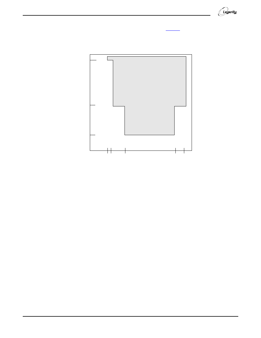
CONNECTION DIAGRAMS
Figure 1. Le58QL02JC 44-Pin PLCC
CD1
3
CD2
3
C3
3
C4
3
CD1
4
CD2
4
C3
4
C4
4
DRB
DRA
VOUT
1
VIN
1
VOUT
2
VIN
2
VCCA
VREF
AGND
VIN
3
VOUT
3
VIN
4
VOUT
4
CD1
2
CD2
2
C3
2
C4
2
CD1
1
CD2
1
C3
1
C4
1
CHCLK
Le58QL02JC
44-Pin PLCC
6
5
4
3
2
1
44
43
42
41 40
29
30
31
32
33
34
35
36
37
38
39
18
19
20
21
22
23
24
25
26
27 28
17
16
15
14
13
12
11
10
9
8
7
MCLK/E1
CS
DCLK
DIO
TSCA
RST
FS
TSCB
DXA
DGND
VCCD
PCLK
DXB
INT

Le58QL02/021/031 VE580 Series Data Sheet
7
Figure 2. Le58QL021JC 44-Pin PLCC
Figure 3. Le58QL031JC 32-Pin PLCC
CD1
3
CD2
3
C3
3
C4
3
C5
3
CD1
4
CD2
4
C3
4
C4
4
C5
4
DRA
VOUT
1
VIN
1
VOUT
2
VIN
2
VCCA
VREF
AGND
VIN
3
VOUT
3
VIN
4
VOUT
4
CD1
2
CD2
2
C3
2
C4
2
C5
2
CD1
1
CD2
1
C3
1
C4
1
Le58QL021JC
44-Pin PLCC
6
5
4
3
2
1
44
43
42
41 40
29
30
31
32
33
34
35
36
37
38
39
18
19
20
21
22
23
24
25
26
27 28
17
16
15
14
13
12
11
10
9
8
7
C5
1
MCLK/E1
CS
DCLK
DIO
RST
TSCA
DXA
DGND
VCCD
PCLK
FS
INT
CD1
2
CD2
2
CD1
1
CD2
1
MCLK/E1
4
3
2
1
32
31
30
29
28
27
26
25
24
23
22
21
5
6
7
8
9
10
11
12
13
14
15
16
17
18
19
20
CD1
3
CD2
3
CD1
4
CD2
4
DRA
VIN
4
VOUT
3
VIN
3
VREF
AGND
VIN
2
VOUT
2
VIN
1
Le58QL031JC
32-Pin PLCC
VOUT
4
VOUT
1
VCCA
CS
INT
DXA
DGND
VCCD
FS
PCLK
DCLK
DIO
TSCA
RST

8
Le58QL02/021/031 VE580 Series Data Sheet
Figure 4. Le58QL021VC 44-Pin PLCC
Le58QL021VC
44-Pin TQFP
12 13 14 15 16 17 18 19 20 21 22
23
24
25
26
27
28
29
30
31
32
33
44 43 42 41 40 39 38 37 36 35 34
5
6
7
8
9
10
11
4
3
2
1
DIO
DCLK
CS
TSCA
DGND
PCLK
VCCD
DXA
FS
RST
INT
VOUT
2
VIN
1
VOUT
1
VIN
2
VCCA
VREF
AGND
VIN
3
VOUT
3
VIN
4
VOUT
4
C3
3
CD2
3
CD1
3
C4
3
C5
3
CD1
4
CD2
4
C3
4
C4
4
C5
4
DRA
C3
2
CD2
2
CD1
2
C4
2
C5
2
CD1
1
CD2
1
C3
1
C4
1
C5
1
MCLK/E1

Le58QL02/021/031 VE580 Series Data Sheet
9
PIN DESCRIPTIONS
Pin Names
Type
Description
AGND, DGND
Power
Separate analog and digital grounds are provided to allow noise isolation; however, the two
grounds are connected inside the part, and the grounds must also be connected together on
the circuit board.
CD1
1
≠CD1
4
,
CD2
1
≠CD2
4
Inputs/Outputs
Control and Data. CD1 and CD2 are TTL compatible programmable Input or Output (I/O)
ports. They can be used to monitor or control the state of the SLIC drivce or any other device
associated with the subscriber line interface. The direction, input or output, is programmed
using MPI Command 54/55h. As outputs, CD1 and CD2 can be used to control relays,
illuminate LEDs, or perform any other function requiring a latched TTL compatible signal for
control. The output state of CD1 and CD2 is written using MPI Command 52h. As inputs, CD1
and CD2 can be processed by the QLSLAC device (if programmed to do so). CD1 can be
debounced before it is made available to the system. The debounce time is programmable
from 0 to 15 ms in 1 ms increments using MPI Command C8/C9h. CD2 can be filtered using
the up/down counter facility and programming the sampling interval using MPI Command E8/
E9h.
Additionally, CD1 can be demultiplexed into two separate inputs using the E1 demultiplexing
function. The E1 demultiplexing function of the QLSLAC device was designed to interface
directly to Legerity SLIC devices supporting the ground key function. With the proper Legerity
SLIC device and the E1 function of the QLSLAC device enabled, the CD1 bit can be
demultiplexed into an Off-Hook/Ring Trip signal and Ground Key signal. In the demultiplex
mode, the second bit, Ground Key, takes the place of the CD2 as an input. The demultiplexed
bits can be debounced (CD1) or filtered (CD2) as explained previously. A more complete
description of CD1, CD2, debouncing, and filtering functions is contained in
Operating the
QLSLAC Device, on page 26
.
Once the CD1 and CD2 inputs are processed (Debounced, Filtered and/or Demultiplexed) by
the QLSLAC device, the information can be accessed by the system in two ways: 1) on a per
channel basis along with C3, C4, and C5 of the specific channel using MPI Command 53h, or
2) by using MPI Command 4D/4Fh, which obtain the CD1 and CD2 bits from all four channels
simultaneously. This feature reduces the processor overhead and the time required to retrieve
time-critical signals from the line circuits, such as off-hook and ring trip. With this feature,
hookswitch status and ring trip information, for example, can be obtained from all four
channels of a QLSLAC device with one read command.
C3
1
≠C3
4
,
C4
1
≠C4
4,
C5
1
≠C5
4
Inputs/Outputs
Control. C3, C4, and C5 are TTL-compatible programmable Input or Output (I/O) ports. They
can be used to monitor or control the state of the SLIC device or any other device associated
with subscriber line interface. The direction, input or output, is programmed using MPI
Command 54/55h. As outputs, C3, C4, and C5 can be used to control relays, illuminate LEDs,
or perform any other function requiring a latched TTL compatible signal for control. The output
state of C3, C4, and C5 is written using MPI Command 52h. As inputs, C3, C4, and C5 can
be accessed by the system by using MPI Command 53h.
The Le58QL021 QLSLAC device contains a single PCM highway and five programmable I/
Os per channel (CD1, CD2, C3, C4, and C5) in a 44-pin PLCC or TQFP package. In the
Le58QL02 QLSLAC device, the C5
1
, C5
2
, C5
3
, and C5
4
I/Os are eliminated, enabling dual
PCM highways and a chopper clock output in a 44-pin PLCC or TQFP package. In the
Le58QL031 QLSLAC device, the C3
1
≠C5
1
, C3
2
≠C5
2
, C3
3
≠C5
3
, and C3
4
≠C5
4
I/Os are
eliminated, enabling a single PCM highway and two control and data I/Os (CD1, CD2) per
channel in a 32-pin PLCC package.
CHCLK
Output
Chopper Clock. This output provides a 256 kHz or a 292.57 kHz, 50% duty cycle, TTL-
compatible clock for use by up to four SLIC devices with built-in switching regulators. The
CHCLK frequency is synchronous to the master clock, but the phase relationship to the master
clock is random. The chopper clock is not available in all package types.
CS
Input
Chip Select. The Chip Select input (active Low) enables the device so that control data can
be written to or read from the part. The channels selected for the write or read operation are
enabled by writing 1 s to the appropriate bits in the Channel Enable Register of the QLSLAC
device prior to the command. See EC1, EC2, EC3, and EC4 of the Command
4A/4Bh Write/
Read Channel Enable and Operating Mode Register, on page 43
for more information. If Chip
Select is held Low for 16 rising edges of DCLK, a hardware reset is executed when Chip
Select returns High.
DCLK
Input
Data Clock. The Data Clock input shifts data into and out of the microprocessor interface of
the QLSLAC device. The maximum clock rate is 8.192 MHz.
DIO
Input/Output
Data. Control data is serially written into and read out of the QLSLAC device via the DIO pin,
with the most significant bit first. The Data Clock determines the data rate. DIO is high
impedance except when data is being transmitted from the QLSLAC device.
10
Le58QL02/021/031 VE580 Series Data Sheet
DRA, DRB
Inputs
PCM Data Receive A/B. The PCM data for channels 1, 2, 3, and 4 is serially received on either
the DRA or DRB port during user-programmed time slots. Data is always received with the
most significant bit first. For compressed signals, 1 byte of data for each channel is received
every 125 µs at the PCLK rate. In the Linear state, two consecutive bytes of data for each
channel are received every 125 µs at the PCLK rate. DRB is not available on all package
types.
DXA, DXB
Outputs
PCM Data Transmit. The transmit data from channels 1, 2, 3, and 4 is sent serially out on
either the DXA or DXB port or both ports during user-programmed time slots. Data is always
transmitted with the most significant bit first. The output is available every 125 µs and the data
is shifted out in 8-bit (16-bit in Linear or PCM Signaling state) bursts at the PCLK rate. DXA
and DXB are High impedance between time slots, while the device is in the Inactive state with
no PCM signaling, or while the Cutoff Transmit Path bit (CTP) is on. DXB is not available on
all package types.
FS
Input
Frame Sync. The Frame Sync pulse is an 8 kHz signal that identifies Time Slot 0, Clock Slot
0 of a system's PCM frame. The QLSLAC device references individual time slots with respect
to this input, which must be synchronized to PCLK.
INT
Output
Interrupt. INT is an active Low output signal which is programmable as either TTL compatible
or open drain. The INT output goes Low any time one of the input bits in the Real Time Data
register changes state and is not masked. It also goes Low any time new transmit data
appears if this interrupt is armed. INT remains Low until the appropriate register is read via
the microprocessor interface, or the QLSLAC device receives either a software or hardware
reset. The individual CD
xy
bits in the Real Time Data register can be masked from causing an
interrupt by using MPI Command 6C/6Dh. The transmit data interrupt must be armed with a
bit in the Operating Conditions register.
MCLK/E1
Input/Output
Master Clock (Input)/Enable CD1 Multiplex (Output). The Master Clock can be a 1.536 MHz,
1.544 MHz, or 2.048 MHz (times 1, 2, or 4) clock for use by the digital signal processor. If the
internal clock is derived from the PCM Clock Input (PCLK), this pin can be used as an E1
output to control Legerity SLIC devices having multiplexed hookswitch and ground-key
detector outputs.
PCLK
Input
PCM Clock. The PCM clock determines the rate at which PCM data is serially shifted into or
out of the PCM ports. PCLK is an integer multiple of the frame sync frequency. The maximum
clock frequency is 8.192 MHz and the minimum clock frequency is 128 kHz for dual PCM
highway versions and 256 kHz for single PCM highway versions. The minimum clock rate
must be doubled if Linear state or PCM signaling is used. PCLK frequencies between 1.03
MHz and 1.53 MHz are not allowed. Optionally, the digital signal processor clock can be
derived from PCLK rather than MCLK.
RST
Input
Reset. A logic Low signal at this pin resets the QLSLAC device to its default state. The RST
pin may be tied to VCCD if it is not needed in the system.
TSCA, TSCB
Outputs
Time Slot Control. The Time Slot Control outputs are open drain outputs (requiring pull-up
resistors to VCCD) and are normally inactive (High impedance). TSCA or TSCB is active
(Low) when PCM data is transmitted on the DXA or DXB pin respectively.
VCCA, VCCD
Power
Analog and digital power supply inputs. VCCA and VCCD are provided to allow for noise
isolation and proper power supply decoupling techniques. For best performance, all of the
VCC power supply pins should be connected together at the connector of the printed circuit
board.
VIN
1
≠VIN
4
Inputs
Analog Input. The analog voice band signal is applied to the VIN input of the QLSLAC device.
The VIN input is biased at VREF by a large internal resistor. The audio signal is sampled,
digitally processed and encoded, and then made available at the TTL-compatible PCM output
(DXA or DXB). If the digitizer saturates in the positive or negative direction, VIN is pulled by a
reduced resistance toward AGND or VCCD, respectively. VIN
1
is the input for channel 1, VIN
2
is the input for channel 2, VIN
3
is the input for channel 3, and VIN
4
is the input for channel 4.
VOUT
1
≠
VOUT
4
Outputs
Analog Output. The received digital data at DRA or DRB is processed and converted to an
analog signal at the VOUT pin. VOUT
1
is the output from channel 1, VOUT
2
is the output for
channel 2, VOUT
3
is the output from channel 3, and VOUT
4
is the output for channel 4. The
VOUT voltages are referenced to VREF.
VREF
Output
Analog Voltage Reference. The VREF output is provided in order for an external capacitor to be
connected from VREF to ground, filtering noise present on the internal voltage reference.
VREF is buffered before it is used by internal circuitry. The voltage on VREF and the output
resistance are given in
Electrical Characteristics, on page 12
. The leakage current in the
capacitor must be low.
Pin Names
Type
Description

Le58QL02/021/031 VE580 Series Data Sheet
11
ABSOLUTE MAXIMUM RATINGS
Stresses above those listed under "Absolute Maximum Ratings" may cause permanent device failure. Functionality at or above
these limits is not implied. Exposure to absolute maximum ratings for extended periods may affect device reliability.
Package Assembly
The green package devices are assembled with enhanced environmental compatible lead (Pb), halogen, and antimony-free
materials. The leads possess a matte-tin plating which is compatible with conventional board assembly processes or newer lead-
free board assembly processes. The peak soldering temperature should not exceed 245∞C during printed circuit board assembly.
Refer to IPC/JEDEC J-Std-020B Table 5-2 for the recommended solder reflow temperature profile.
OPERATING RANGES
Legerity guarantees the performance of this device over commercial (0 to 70∫ C) and industrial (-40 to 85∫C) temperature ranges
by conducting electrical characterization over each range and by conducting a production test with single insertion coupled to
periodic sampling. These characterization and test procedures comply with section 4.6.2 of Bellcore GR-357-CORE Component
Reliability Assurance Requirements for Telecommunications Equipment.
Environmental Ranges
Electrical Ranges
Storage Temperature
≠60∞ C
< T
A
< +125∞ C
Ambient Temperature, under Bias
≠40∞ C
< T
A
< +85∞ C
Ambient relative humidity (non condensing)
5 to 95%
V
CCA
with respect to AGND
≠0.4 to + 4.0 V
V
CCA
with respect to VCCD
±0.4 V
V
CCD
with respect to DGND
≠0.4 to + 4.0 V
V
IN
with respect to AGND
≠0.4 V to (V
CCA
+ 0.4 V)
AGND with respect to DGND
±50 mV
Digital pins with respect to DGND
≠0.4 to 5.5 V or VCCD + 2.37 V, whichever is
smaller
Total combined CD1≠C5 current per device:
Source from VCCD
40 mA
Sink into DGND
40 mA
Latch up immunity (any pin)
± 100 mA
Total VCC current if rise rate of VCC > 0.4 V/µs
0.5 A
Ambient Temperature
≠40∞ C
< T
A
< +85∞ C
Ambient Relative Humidity
15 to 85%
Analog Supply V
CCA
+3.3 V ± 5%
V
CCD
± 50 mV
Digital Supply V
CCD
+3.3 V ± 5%
DGND
0 V
AGND
±10 mV
CFIL Capacitance: VREF to AGND
0.1 µF ± 20%
Digital Pins
DGND to +5.25 V

12
Le58QL02/021/031 VE580 Series Data Sheet
ELECTRICAL CHARACTERISTICS
Typical values are for TA = 25∫ C and nominal supply voltages. Minimum and maximum values are over the temperature and
supply voltage ranges shown in Operating Ranges, except where noted.
Symbol
Parameter Descriptions
Min
Typ
Max
Unit
Note
V
IL
Digital Input Low voltage
0.8
V
V
IH
Digital Input High voltage
2.0
I
IL
Digital Input leakage current
µA
0
< V < VCCD
≠7
+7
Otherwise
≠120
+180
V
HYS
Digital Input hysteresis
0.16
0.25
0.34
V
V
OL
Digital Output Low voltage
CD1≠C5 (I
OL
= 4 mA)
CD1≠C5 (I
OL
= 8 mA)
TSCA, TSCB (I
OL
=14 mA)
Other digital outputs (I
OL
= 2 mA)
0.4
0.8
0.4
0.4
V
1
V
OH
Digital Output High voltage
CD1≠C5 (I
OH
= 4 mA)
CD1≠C5 (I
OH
= 8 mA)
Other digital outputs (I
OH
= 400
µA)
V
CCD
≠ 0.4 V
V
CCD
≠ 0.8 V
2.4
V
1
I
OL
Digital Output leakage current (H
I
Z state)
0
< V < VCCD
≠7
+7
µA
Otherwise
≠120
+180
GIN
Input attenuator gain
DGIN = 0
DGIN = 1
0.6438
1
V/V
V
IR
Analog input voltage range (Relative to VREF)
AX = 0 dB, attenuator on (DGIN = 0)
AX = 6.02 dB, attenuator on (DGIN = 0)
AX = 0 dB, attenuator off (DGIN = 1)
AX = 6.02 dB, attenuator off (DGIN = 1)
±1.584
±0.792
±1.02
±0.51
Vpk
V
IOS
Offset voltage allowed on VIN
≠50
50
mV
Z
IN
Analog input impedance to VREF, 300 to 3400 Hz
600
1400
k
I
IP
Current into analog input for an input voltage of 3.3 V
50
115
µA
2
I
IN
Current out of analog input for an input voltage of ≠0.3 V
50
130
2
Z
OUT
VOUT output impedance
1
10
CL
OUT
Allowable capacitance, V
OUT
to AGND
500
pF
I
OUT
VOUT
output current (F< 3400 Hz)
≠4
4
mApk
3
V
REF
VREF output open circuit voltage (leakage < 20 nA)
1.43
1.5
1.57
V
Z
REF
VREF output impedance (F < 3400 Hz)
70
130
k
V
OR
VOUT voltage range(AR = 0 dB)
(Relative to VREF)(AR = 6.02 dB)
±1.02
±0.51
Vpk
V
OOS
VOUT offset voltage (AISN off)
≠40
40
mV
4
V
OOSA
VOUT offset voltage (AISN on)
≠80
80
G
AISN
AISN gain - expected gain (input = 0 dBm0, 1014 Hz)
Attenuator on (DGIN = 0)
Attenuator off (DGIN = 1)
≠0.016
≠0.024
0.016
0.024
V/V
PD
Power dissipation
All channels active
1 channel active
All channels inactive
130
40
13
170
80
18
mW
C
I
Digital Input capacitance
10
pF
C
O
Digital Output capacitance
10
PSRR
Power supply rejection ratio (1.02 kHz, 100 mV
RMS
, either
path, GX = GR = 0 dB)
40
dB

Le58QL02/021/031 VE580 Series Data Sheet
13
Notes:
1.
The CD1, CD2, C3≠C5 outputs are resistive for less than a 0.8 V drop. Total current must not exceed absolute maximum ratings.
2.
When the digitizer saturates, a resistor of 50 k
±20 k is connected either to AGND or to VCCA as appropriate to discharge the coupling
capacitor.
3.
When the QLSLAC device is in the Inactive state, the analog output will present either a VREF DC output level through a 15 k
resistor
(VMODE = 0) or a high impedance (VMODE = 1).
4.
If there is an external DC path from VOUT to VIN with a gain of G
DC
and the AISN has a gain of h
AISN
, then the output offset will be multiplied
by 1 / [1 ≠ (h
AISN
∑ G
DC
)].
5.
Power dissipation in the Inactive state is measured with all digital inputs at VIH = VCCD and VIL = DGND and with no load connected to
VOUT1, VOUT2, VOUT3, or VOUT4.
Transmission Characteristics
When relative levels (dBm0) are used in any of the following transmission specifications, the specification holds for any setting
of the GX gain from 0 dB to 12 dB, the GR loss from 0 dB to 12 dB, and the input attenuator (GIN) on or off.
Notes:
1.
See Figure 5 and Figure 6.
2.
0 dBm0 input signal, 300 Hz to 3400 Hz; measurement at any other frequency, 300 Hz to 3400 Hz.
3.
No single frequency component in the range above 3800 Hz may exceed a level of ≠55 dBm0.
4.
The weighted average of the crosstalk is defined by the following equation, where C(f) is the crosstalk in dB as a function of frequency, f
N
= 3300 Hz, f
1
= 300 Hz, and the frequency points (f
j
, j = 2..N) are closely spaced:
Table 2. 0 dBm0 Voltage Definitions with Unity Gain in X, R, GX, GR, AX, and AR
Signal at Digital Interface
Transmit
(DGIN = 0)
Transmit
(DGIN = 1)
Receive
Unit
A-law digital mW or equivalent (0 dBm0)
0.7804
0.5024
0.5024
Vrms
µ-law digital mW or equivalent (0 dBm0)
0.7746
0.4987
0.4987
±22,827 peak linear coded sine wave
0.7804
0.5024
0.5024
Description
Test Conditions
Min
Typ
Max
Unit
Note
Gain accuracy, D/A or A/D
0 dBm0, 1014 Hz
AX = AR = 0 dB
0 to 85∞ C
≠40∞ C
AX = +6.02 dB and/or
AR = ≠6.02 dB
0 to 85∞ C
≠40∞ C
≠0.25
≠0.30
≠0.30
≠0.40
+0.25
+0.30
+0.30
+0.40
dB
Gain accuracy digital-to-digital
≠0.25
+0.25
Gain accuracy analog-to-analog
≠0.25
+0.25
Attenuation distortion
300 Hz to 3 kHz
≠0.125
+0.125
1
Single frequency distortion
≠46
2
Second harmonic distortion, D-A
GR = 0 dB
≠55
Idle channel noise
Analog out
Digital out
Digital looped back
weighted
unweighted
Digital input = 0
A-law
Digital input = 0
µ-law
Analog V
IN
= 0 VAC
A-law
Analog V
IN
= 0 VAC
µ-law
0
0
≠68
≠55
≠78
12
≠68
16
dBm0p
dBm0
dBm0p
dBrnc0
dBm0p
dBrnc0
3
3
3
3, 6
3
3, 6
Crosstalk
TX to RX
same channel
RX to TX
0 dBm0
300 to 3400 Hz
0 dBm0
300 to 3400 Hz
≠75
≠75
dBm0
Crosstalk between channels
TX or RX to TX
TX or RX to RX
0 dBm0
SLIC imped. < 300
1014 Hz, Average
1014 Hz, Average
≠76
≠78
dBm0
4
End-to-end group delay
B = Z = 0; X = R = 1
678
µs
5

14
Le58QL02/021/031 VE580 Series Data Sheet
5.
The End-to-End Group Delay is the sum of the transmit and receive group delays (both measured using the same time and clock slot).
6.
Typical values not tested in production.
Attenuation Distortion
The signal attenuation in either path is nominally independent of the frequency. The deviations from nominal attenuation will stay
within the limits shown in
Figure 5
and
Figure 6
. The reference frequency is 1014 Hz and the signal level is
≠
10 dBm0.
Figure 5. Transmit Path Attenuation vs. Frequency
Figure 6. Receive Path Attenuation vs. Frequency
Average
20
10
1
20
------ C f
j
( )
∑
10
1
20
------ C f
j 1
≠
(
)
∑
+
2
----------------------------------------------------------------
f
j
f
j 1
≠
----------
log
∑
j
f
N
f
1
-----
log
---------------------------------------------------------------------------------------------------------
log
∑
=
3
000
3
400
Acceptable Region
0.75
3
00
2
00
Frequency (Hz)
0
0
-0.125
0.125
Attenuation (dB)
0
1.8
3
000
3
400
2
0.6
Acceptable Region
0.65
6
00
3
00
2
00
0
3
200
0.80
0.2
Attenuation (dB)
1
Frequency (Hz)
0
-0.125
0.125
Le58QL02/021/031 VE580 Series Data Sheet
15
Group Delay Distortion
For either transmission path, the group delay distortion is within the limits shown in
Figure 7
. The minimum value of the group
delay is taken as the reference. The signal level should be 0 dBm0.
Figure 7. Group Delay Distortion
0
500
600
1
000
2
600
2
800
90
150
420
Delay (µS)
Acceptable
Region
Frequency (Hz)

16
Le58QL02/021/031 VE580 Series Data Sheet
Gain Linearity
The gain deviation relative to the gain at ≠10 dBm0 is within the limits shown in
Figure 8
(A-law) and
Figure 9
(
µ
-law) for either
transmission path when the input is a sine wave signal of 1014 Hz.
Figure 8. A-law Gain Linearity with Tone Input (Both Paths)
Figure 9.
µ
-law Gain Linearity with Tone Input (Both Paths)
0.55
0.25
0
-0.25
-0.55
-1.5
-55 -50
-40
-10
1.5
Gain (dB)
0
Acceptable Region
Input
Level
(dBm0)
+3
0.45
0.25
0
-0.25
-0.45
-1.4
-55 -50
-37
-10
1.4
Gain (dB)
0
Acceptable Region
+3
Input
Level
(dBm0)
Le58QL02/021/031 VE580 Series Data Sheet
17
Total Distortion Including Quantizing Distortion
The signal to total distortion ratio will exceed the limits shown in
Figure 10
for either path when the input signal is a sine wave
signal of frequency 1014 Hz.
Figure 10. Total Distortion with Tone Input (Both Paths)
Input Level (dBm0)
Signal-to-Total
Distortion (dB)
Acceptable Region
0
-30
-40
-45
A
A-Law µ-Law
A 35.5dB 35.5dB
B 35.5dB 35.5dB
C 30dB 31dB
D 25dB 27dB
B
C
D

18
Le58QL02/021/031 VE580 Series Data Sheet
Discrimination Against Out-of-Band Input Signals
When an out-of-band sine wave signal of frequency f, and level A is applied to the analog input, there may be frequency
components below 4 kHz at the digital output which are caused by the out-of-band signal. These components are at least the
specified dB level below the level of a signal at the same output originating from a 1014 Hz sine wave signal with a level of A
dBm0 also applied to the analog input. The minimum specifications are shown in the following table.
Figure 11. Discrimination Against Out-of-Band Signals
Note:
The attenuation of the waveform below amplitude A, between 3400 Hz and 4600 Hz, is given by the formula:
Discrimination Against 12- and 16-kHz Metering Signals
If the QLSLAC device is used in a metering application where 12 kHz or 16 kHz tone bursts are injected onto the telephone line
toward the subscriber, a portion of these tones also may appear at the VIN terminal. These out-of-band signals may cause
frequency components to appear below 4 kHz at the digital output. For a 12 kHz or 16 kHz tone, the frequency components below
4 kHz are reduced from the input by at least 70 dB. The sum of the peak metering and signal voltages must be within the analog
input voltage range.
Frequency of Out-of-Band Signal
Amplitude of Out-of-Band Signal
Level below A
16.6 Hz < f < 45 Hz
≠25 dBm0 < A
0 dBm0
18 dB
45 Hz < f < 65 Hz
≠25 dBm0 < A
0 dBm0
25 dB
65 Hz < f < 100 Hz
≠25 dBm0 < A
0 dBm0
10 dB
3400 Hz < f < 4600 Hz
≠25 dBm0 < A
0 dBm0
see Figure 11
4600 Hz < f < 100 kHz
≠25 dBm0 < A
0 dBm0
32 dB
0
-10
-20
-30
-40
Level below
A (dB)
-50
3.4
4.0
4.6
Frequency (kHz)
-28 dB
-32 dB
Attenuation (db)
14 14
4000 f
≠
(
)
1200
-----------------------------
sin
≠
=

Le58QL02/021/031 VE580 Series Data Sheet
19
Spurious Out-of-Band Signals
at the Analog Output
With PCM code words representing a sine wave signal in the range of 300 Hz to 3400 Hz at a level of 0 dBm0 applied to the
digital input, the level of the spurious out-of-band signals at the analog output is less than the limits shown below.
With code words representing any sine wave signal in the range 3.4 kHz to 4.0 kHz at a level of 0 dBm0 applied to the digital
input, the level of the signals at the analog output are below the limits in
Figure 12
. The amplitude of the spurious out-of-band
signals between 3400 Hz and 4600 Hz is given by the formula:
Figure 12. Spurious Out-of-Band Signals
Frequency
Level
4.6 kHz to 40 kHz
≠32 dBm0
40 kHz to 240 kHz
≠46 dBm0
240 kHz to 1 MHz
≠36 dBm0
Level
14
≠
14
f 4000
≠
(
)
1200
-----------------------------
sin
≠
dBm0
=
0
-10
-20
-30
-40
Level (dBm0)
-50
3.4
4.0
4.6
Frequency (kHz)
-28 dBm0
-32 dBm0

20
Le58QL02/021/031 VE580 Series Data Sheet
Overload Compression
Figure 13
shows the acceptable region of operation for input signal levels above the reference input power (0 dBm0). The
conditions for this figure are:
1.
1.2 dB < GX
+ 12 dB
2.
≠12 dB
GR < ≠1.2 dB
3.
Digital voice output connected to digital voice input.
4.
Measurement analog-to-analog.
Figure 13. Analog-to-Analog Overload Compression
Fundamental
Output Power
(dBm0)
Fundamental Input Power (dBm0)
1
2
3
4
5
6
7
8
9
1
2
3
4
5
6
7
8
9
2.6
Region
Acceptable

Le58QL02/021/031 VE580 Series Data Sheet
21
SWITCHING CHARACTERISTICS
The following are the switching characteristics over operating range (unless otherwise noted). Min and max values are valid for
all digital outputs with a 115 pF load, except CD1≠C5 with a 30 pF load. (See Figure 15 and Figure 16 for the microprocessor
interface timing diagrams.)
Microprocessor Interface
PCM Interface
PCLK not to exceed 8.192 MHz.
Pull-up resistors to V
CCD
of 240
are attached to TSCA and TSCB. (See Figure 17 and Figure 18 for the PCM interface timing
diagrams.)
No.
Symbol
Parameter
Min
Typ
Max
Unit
Note
1
t
DCY
Data clock period
122
ns
2
t
DCH
Data clock HIGH pulse width
48
3
t
DCL
Data clock LOW pulse width
48
4
t
DCR
Rise time of clock
25
5
t
DCF
Fall time of clock
25
6
t
ICSS
Chip select setup time, Input mode
30
t
DCY
≠10
7
t
ICSH
Chip select hold time, Input mode
0
t
DCH
≠20
8
t
ICSL
Chip select pulse width, Input mode
8t
DCY
9
t
ICSO
Chip select off time, Input mode
2500
1
10
t
IDS
Input data setup time
25
11
t
IDH
Input data hold time
30
12
t
OLH
SLIC device output latch valid
2500
13
t
OCSS
Chip select setup time, Output mode
30
t
DCY
≠10
14
t
OCSH
Chip select hold time, Output mode
0
t
DCH
≠20
15
t
OCSL
Chip select pulse width, Output mode
8t
DCY
16
t
OCSO
Chip select off time, Output mode
2500
1
17
t
ODD
Output data turn on delay
50
2
18
t
ODH
Output data hold time
3
19
t
ODOF
Output data turn off delay
50
20
t
ODC
Output data valid
50
21
t
RST
Reset pulse width
50
µs
No.
Symbol
Parameter
Min.
Typ
Max
Unit
Note
22
t
PCY
PCM clock period
122
ns
3
23
t
PCH
PCM clock HIGH pulse width
48
24
t
PCL
PCM clock LOW pulse width
48
25
t
PCF
Fall time of clock
15
26
t
PCR
Rise time of clock
15
27
t
FSS
FS setup time
25
t
PCY
≠30
28
t
FSH
FS hold time
50
30
t
TSD
Delay to TSC valid
5
80
4
31
t
TSO
Delay to TSC off
5
80
4, 5
32
t
DXD
PCM data output delay
5
70
33
t
DXH
PCM data output hold time
5
70
34
t
DXZ
PCM data output delay to High-Z
5
70
35
t
DRS
PCM data input setup time
25
36
t
DRH
PCM data input hold time
5

22
Le58QL02/021/031 VE580 Series Data Sheet
Master Clock
(See
Figure 19, Master Clock Timing, on page 25
.)
Auxiliary Output Clocks
Notes:
1.
If CFAIL = 1 (Command 55h), GX, GR, Z, B1, X, R, and B2 coefficients must not be written or read without first deactivating all channels or
switching them to default coefficients; otherwise, a chip select off time of 25 µs is required.
2.
The first data bit is enabled on the falling edge of CS or on the falling edge of DCLK, whichever occurs last.
3.
The PCM clock frequency must be an integer multiple of the frame sync frequency. The maximum allowable PCM clock frequency is 8.192
MHz. The actual PCM clock rate is dependent on the number of channels allocated within a frame. The minimum clock frequency is 128
kHz in Companded state and 256 kHz in Linear state, PCM Signaling state, or double PCLK state. The minimum PCM clock rates should
be doubled for parts with only one PCM highway in order to allow simultaneous access to all four channels.
4.
TSC is delayed from FS by a typical value of N ∑ t
PCY
, where N is the value stored in the time/clock-slot register.
5.
t
TSO
is defined as the time at which the output achieves the Open Circuit state.
6.
PCLK and MCLK are required to be integer multiples of the frame sync (FS) frequency. Frame sync is expected to be an accurate 8 kHz
pulse train. If PCLK or MCLK has jitter, care must be taken to ensure that all setup, hold, and pulse width requirements are met.
7.
Phase jumps of 81 nS will be present when the master clock frequency is a multiple of 1.544 MHz.
No.
Symbol
Parameter
Min
Typ
Max
Unit
Notes
37
J
MCY
Master clock jitter
50
ns
6
38
t
MCR
Rise time of clock
15
39
t
MCF
Fall time of clock
15
40
t
MCH
MCLK HIGH pulse width
48
41
t
MCL
MCLK LOW pulse width
48
No.
Symbol
Parameter
Min
Typ
Max
Unit
Notes
42
f
CHP
Chopper clock frequency
CHP = 0
CHP = 1
256
292.57
kHz
7
42A
DC
CHP
Chopper click duty cycle
50
%
7
43
f
E1
E1 output frequency (CMODE = EE1 = 1)
4.923
kHz
7
44
t
E1
E1 pulse width (CMODE = EE1 = 1)
31.25
µs
7

Le58QL02/021/031 VE580 Series Data Sheet
23
SWITCHING WAVEFORMS
Figure 14. Input and Output Waveforms for AC Tests
Figure 15. Microprocessor Interface (Input Mode)
2.0 V
0.8 V
TEST
POINTS
2.4 V
0.45 V
2.0 V
0.8 V
1
5
V
IL
DCLK
4
CS
Data
Valid
11
D
I/O
2
3
6
8
10
7
Data
Valid
V
IH
V
IL
V
IH
9
12
Data
Valid
Data
Valid
Data
Valid
Outputs
C5 - C1
24
Le58QL02/021/031 VE580 Series Data Sheet
Figure 16. Microprocessor Interface (Output Mode)
Figure 17. PCM Highway Timing for XE = 0 (Transmit on Negative PCLK Edge)
DCLK
Data
Valid
Data
Valid
D
I/O
Three-State
V
OL
V
OH
Data
Valid
Three-State
V
IH
V
IL
CS
13
17
20
18
15
14
16
19
First Bit
PCLK
FS
DXA/DXB
DRA/DRB
First
Bit
Second
Bit
V
OL
V
OH
V
IH
V
IL
V
IH
V
IL
TSCA/
TSCB
Time Slot Zero
Clock Slot Zero
27
25
22
26
30
24
28
23
32
33
35
36
34
31

Le58QL02/021/031 VE580 Series Data Sheet
25
Figure 18. PCM Highway Timing for XE = 1 (Transmit on Positive PCLK Edge)
Figure 19. Master Clock Timing
Time Slot Zero
Clock Slot Zero
First Bit
PCLK
FS
DXA/DXB
DRA/DRB
First
Bit
Second
Bit
V
OL
V
OH
TSCA/
TSCB
V
IH
V
IL
V
IH
V
IL
22
25
31
34
33
35
36
27
30
32
28
23
24
26
V
IL
V
IH
40
37
41
39
38

26
Le58QL02/021/031 VE580 Series Data Sheet
OPERATING THE QLSLAC DEVICE
The following sections describe the operation of the four independent channels of the QLSLAC device. The description is valid
for channel 1, 2, 3, or 4; consequently, the channel subscripts have been dropped. For example, VOUT refers to either VOUT1,
VOUT2, VOUT3, or VOUT4.
Power-Up Sequence
The recommended QLSLAC device power-up sequence is to apply:
1.
Analog and digital ground
2.
VCC, signal connections, and Low on RST
3.
High on RST
The software initialization should then include:
1.
Wait 1 ms.
2.
Select master clock frequency and source (Command 46/47h). This should turn off the CFAIL bit (Command 55h) within
400 µs.
3.
Program filter coefficients and other parameters as required.
4.
Activate (Command 0Eh).
If the power supply (VCCD) falls below an internal threshold, the device is reset and will require complete reprogramming with
the above sequence. A reset may be initiated by connection of a logic Low to the RST pin, or if chip select (CS) is held low for
16 rising edges of DCLK, a hardware reset is generated when CS returns high. The RST pin may be tied to VCCD if it is not used
in the system.
Channel Enable (EC) Register
A channel enable register has been implemented in the QLSLAC device in order to reduce the effort required to address
individual or multiple channels of the QLSLAC device. The register is written using MPI Command 4A/4Bh. Each bit of the register
is assigned to one unique channel, bit 0 for channel 1, bit 1 for channel 2, bit 2 for channel 3, and bit 3 for channel 4. The channel
or channels are enabled when their corresponding enable bits are High. All enabled channels will receive the data written to the
QLSLAC device. This enables a Broadcast mode (all channels enabled) to be implemented simply and efficiently, and multiple
channel addressing is accomplished without increasing the number of I/O pins on the device. The Broadcast mode can be further
enhanced by providing the ability to select many chips at once; however, care must be taken not to enable more than one chip
in the Read state. This can lead to an internal bus contention, in which excess power is dissipated. (Bus contention will not
damage the device.)
SLIC Device Control and Data Lines
The QLSLAC device has up to five SLIC device programmable digital input/output pins per channel (CD1≠C5). Each of these
pins can be programmed as either an input or an output using the I/O Direction register, Command 54/55h (see Figure 21). The
output latches can be written with Command 52h; however, only those bits programmed as outputs will actually drive the pins.
The inputs can be read with Command 53h. If a pin is programmed as an output, the data read from it will be the contents of the
output latch. It is recommended that any of the SLIC device input/output control and data pins, which are to be programmed as
outputs, be written to their desired state via Command 52h before writing the data which configures them as outputs with the I/
O direction register Command 54/55h. This ensures that when the output is activated, it is already in the correct state, and will
prevent unwanted data from being driven from the SLIC device output pins. It is possible to make a SLIC device control output
pull up to a non-standard voltage (V
< 5.25 V) by connecting a resistor from the output to the desired voltage, sending zero to the
output, and using the DIO bit to tri-state the output.
Clock Mode Operation
The QLSLAC device operates with multiple clock signals. The master clock is used for internal timing including operation of the
digital signal processing and may be derived from either the MCLK or PCLK source. When MCLK is used as the master clock, it
should be synchronous to FS. The allowed frequencies are listed under Command 46/47h.
The PCM clock (PCLK) is used for PCM timing and is an integer multiple of the frame sync frequency. The internal master clock
can be optionally derived from the PCLK source by setting the CMODE bit (bit 4, Command 46/47h) to one. In this mode, the
MCLK/E1 pin is free to be used as an E1 signal output. Clock mode options and E1 output functions are shown in Figure 20.

Le58QL02/021/031 VE580 Series Data Sheet
27
Figure 20. Clock Mode Options
.
E1 Multiplex Operation
The QLSLAC device can multiplex input data from the CD1 SLIC device I/O pin into two separate status bits per channel (CD1
and CD1B bits in the SLIC Input/Output register, Command 52/53h, and CDA and CDB bits in the Real Time Data register,
Command 4D/4Fh) using the E1 multiplex mode. This multiplex mode provides the means to accommodate dual detect states
when connected to an Legerity SLIC device, which also supports ground-key detection in addition to loop detect. Legerity SLIC
devices that support ground-key detect use their E1 pin as an input to switch the SLIC device's single detector (DET) output
between internal loop detect or ground-key detect comparators. Using the E1 multiplex mode, a single QLSLAC device can
monitor both loop detect and ground-key detect states of all four connected SLIC devices without additional hardware. Although
normally used for ground key detect, this multiplex function can also be used for monitoring other signal states.
The E1 multiplex mode is selected by setting the EE1 bit (bit 7, Command C8/C9h) and the CMODE bit (bit 4, Command
46/47h) in the QLSLAC device. The CMODE bit must be selected (CMODE=1) for the master clock to be derived from PCLK so
that the MCLK/E1 pin can be used as an output for the E1 signal. The multiplex mode is then turned on by setting the EE1 bit.
With the E1 multiplex mode enabled, the QLSLAC device generates the E1 output signal. This signal is a 31.25
µ
s (1/32 kHz)
duration pulse occurring at a 4.923 kHz (64 kHz/13) rate. If EE1 is reset, MCLK/E1 is programmed as an input and should be
connected to ground if it is not connected to a clock source. The polarity of this E1 output is selected by the E1P bit (bit 6,
Command C8/C9h) allowing this multiplex mode to accommodate all SLIC devices regardless of their E1 high/low logic definition.
Figure 21 shows the SLIC device Input/Output register, I/O pins, E1 multiplex hardware operation for one QLSLAC device
channel. It also shows the operation of the Real Time Register. The QLSLAC device E1 output signal connects directly to the E1
inputs of all four connected SLIC devices and is used by those SLIC devices to select an internal comparator to route to the SLIC
device DET output. This E1 signal is also used internally by the QLSLAC device for controlling the multiplex operation and timing.
The CD1 and CD1B bits of the SLIC device Input/Output register are isolated from the CD1 pin by transparent latches. When the
E1 pulse is off, the CD1 pin data is routed directly to the CD1 bit of the SLIC device I/O register and changes to the CD1B bit of
that register are disabled by its own latch. When E1 pulses on, the CD1 latch holds the last CD1 state in its register. At the same
time, the CD1B latch is enabled, which allows CD1 pin data to be routed directly to the CD1B bit. Therefore, during this
multiplexing, the CD1 bit always has loop-detect status and the CD1B bit always has ground-key detect status.
This multiplexing state changes almost instantaneously within the QLSLAC device but the SLIC device may require a slightly
longer time period to respond to this detect state change before its DET output settles and becomes valid. To accommodate this
delay difference, the internal signals within the QLSLAC device are isolated by 15.625
µ
s before allowing any change to the CD1
bit and CD1B bit latches. This operation is further described by the E1 multiplex timing diagram in Figure 22. In this timing
diagram, the E1 signal represents the actual signal presented to the E1 output pin. The GK Enable pulse allows CD1 pin data to
Time
Slot
Assigner
DSP
Engine
E1
Pulses
E1P
PCLK
MCLK/E1
N
˜
CSEL
CMODE
(= 1)
(= 0)
E1
(= 1)
(= 0)
EE1
Notes:
1. CMODE = Command 46/47h
Bit 4
2. CSEL = Command 46/47h
Bits 0≠3
3. EE1 = Command C8/C9h
Bit 7
4. E1P = Command C8/C9h
Bit 6
(= 0)
(= 1)

28
Le58QL02/021/031 VE580 Series Data Sheet
be routed through the CD1B latch. The LD Enable pulse allows CD1 pin data to be routed through the CD1 latch. The uncertain
states of the SLIC device's DET output, and the masked times where that DET data is ignored are shown in this timing diagram.
Using this isolation of masked times, the CD1 and CD1B registers are guaranteed to contain accurate representations of the
SLIC device detector output.
Figure 21. SLIC Device I/O E1 Multiplex and Real-Time Data Register Operation
Note:
* Transparent latches: When enable input is high, Q output follows D input. When enable input goes low, Q output is latched at last state.
--
-- CD1B C5
C4
C3 CD2 CD1
D
Q
EN/HOLD
CD1
CD2
C3
C4
C5
D
Q
EN/HOLD
0
1
Output Latch
I/O Direction
MPI Command
Register
EE1 Bit
SLIC Output
Register
MPI Command 52h
SLIC Input Register
MPI Command 53h
LD Enable
*
Delay
GK Enable
*
E1 Source
E1P
MCLK/E1
MUX
CDB
1
CDA
1
Real Time
Data Register
(Command 4D/4Fh)
Interrupt Mask
Register
(Command 6C/6Dh)
(Channel 1
Shown)
{
Same for
Channels
2, 3, 4
(Command 70/71h)
ATI
Ground Key Filter
(time set via Command
E8/E9h)
MCDB
1
MCDA
1
Debounce
(time set via Command
C8/C9h)
INT
(Internal)
See Figure 22
for details
CDA
4
CDA
3
CDA
2
CDB
4
CDB
3
CDB
2
MCDB
4
MCDA
4
MCDB
3
MCDA
3
MCDB
2
MCDA
2
54/55h

Le58QL02/021/031 VE580 Series Data Sheet
29
Figure 22. E1 Multiplex Internal Timing
Debounce Filters Operation
Each channel is equipped with two debounce filter circuits to buffer the logic status of the CD1 and CD2/CD1B bits of the SLIC
device Input Data Register (Command 53h) before providing filtered bit's outputs to the Real-Time Data Register (Command 4D/
4Fh). One filter is used only for the CD1 bit. The other filter acts upon either the CD1B bit if E1 multiplexing is enabled, or on the
CD2 bit if the multiplexing is not enabled.
The CD1 bit normally contains SLIC device loop detect status. The CD1 debouncing time is programmable with the Debounce
Time Register (Command C8/C9h), and even though each channel has its own filter, the programmed value is common to all
four channels. This debounce filter is initially clocked at the frame sync rate of 125
µs, and any occurrence of changing data at
this sample rate resets a programmable counter. This programmable counter is clocked at a 1 ms rate, and the programmed
count value of 0 to 15 ms, as defined by the Debounce Time Register, must be reached before updating the CDA bit of the Real
Time Data register with the CD1 state. Refer to
Figure 23
a for this filter's operation.
The ground-key filter (Figure 23b) provides a buffering of the signal, normally ground key detect, which appears in the CD1B bit
of the Real Time Data Register. Each channel has its own filter, and each filter's time can be individually programmed. The input
to the filter comes from either the CD2 bit of the SLIC device I/O Data Register (Command 53h), when E1 multiplexing is not
enabled, or from the CD1B bit of that register when E1 multiplexing is enabled. The feature debounces ground-key signals before
passing them to the Real Time Data Register, although signals other than ground-key status can be routed to the CD2 pin and
then through the registers.
The ground-key debounce filter operates as a duty-cycle detector and consists of an up/down counter which can range in value
between 0 and 6. This six-state counter is clocked by the GK timer at the sampling period of 1≠15 ms, as programmed by the
value of the four GK bits (GK3, GK2, GK1, GK0) of the Ground-Key Filter Data register (Command E8/E9h). This sampling period
clocks the counter, which buffers the CD2/CD1B bit's status before it is valid for presenting to the CDB bit of the Real Time Data
Register. When the sampled value of the ground-key (or CD2) input is high, the counter is incremented by each clock pulse. When
the sampled value is low, the counter is decremented. Once the counter increments to its maximum value of 6, it sets a latch
whose output is routed to the corresponding CDB bit. If the counter decrements to its minimum value of 0, this latch is cleared
and the output bit is set to zero. All other times, the latch (and the CDB status) remains in its previous state without change. It
therefore takes at least six consecutive GK clocks with the debounce input remaining at the same state to effect an output
change. If the GK bit value is set to zero, the buffering is bypassed and the input status is passed directly to CDB.
31.25
µs
4.923 kHz (64 kHz/13) pulse rate
15.625
µs
E1
GK Enable
LD Enable
15.625
µs
15.625
µs
Pulse Period 203.125
µs
DET Output
from SLIC
(CD1 Pin Input)
Contains
Valid GK
Status
Contains
Valid LD
Status
Contains
Valid LD
Status
CD1 Pin
State
Ignored
CD1 Pin
State
Ignored
CD1 Pin
Input Data
Hold Last State
Tracks
DET State
CD1
Register
Operation
Tracks
DET State
CD1B
Register
Operation
Hold Last State
Tracks
DET State
Hold Last State

30
Le58QL02/021/031 VE580 Series Data Sheet
Figure 23. MPI Real-Time Data Register
a. Loop Detect Debounce Filter
Notes:
*Transparent latch: Output follows input when EN is high; ouput holds last state when EN is low.
Debounce counter: Output is high after counting to programmed (DSH) number of 1 ms clocks; counter is reset for CD1 input changes at 125 µs
sample period. DSH0 - DSH3 programmed value is common for all four channels, but debounce counter is separate per channel.
b. Ground-Key Filter
Notes:
Programmed value of GK0 - GK3 determines clock rate (1 - 15 ms) of six-state counter.
If GK value = 0, the counter is bypassed and no buffering occurs.
Six-state up/down counter: Counts up when input is high; counts down when input is low.
Output goes and stays high when maximum count is reached; output goes and stays low when count is down to zero.
Real-Time Data Register Operation
To obtain time-critical data such as off/on-hook and ring trip information from the SLIC device with a minimum of processor time
and effort, the QLSLAC device contains an 8-bit Real Time Data register. This register contains CDA and CDB bits from all four
channels. The CDA bit for each channel is a debounced version of the CD1 input. The CDA bit is normally used for hook switch.
The CDB bit for each channel normally contains the debounced value of the CD2 input bit; however, if the E1 multiplex operation
is enabled, the CDB bit will contain the debounced value of the CD1B bit. CD1 and CD2 can be assigned to off-hook, ring trip,
ground key signals, or other signals. Frame sync is needed for the debounce and the ground key signals. If Frame sync is not
provided, the real-time register will not work. The register is read using MPI Command 4D/4Fh, and may be read at any time
regardless of the state of the Channel Enable Register. This allows off/on-hook, ring trip, or ground key information for all four
channels to be obtained from the QLSLAC device with one read operation versus one read per channel. If these data bits are not
used for supervision information, they can be accessed on an individual channel basis in the same way as C3≠C5; however, CD1
and CD1B will not be debounced.
Interrupt
In addition to the Real Time Data register, an interrupt signal has been implemented in the QLSLAC device. The interrupt signal
is an active Low output signal which pulls Low whenever the unmasked CD bits change state (Low to High or High to Low); or
whenever the transmit PCM data changes on a channel in which the Arm Transmit Interrupt (ATI) bit is on. The interrupt control
is shown in
Figure 21
. The interrupt remains Low until the appropriate register is read. This output can be programmed as TTL
or open drain. When an interrupt is generated, all of the unmasked bits in the Real Time Data register latch and remain latched
until the interrupt is cleared. The interrupt is cleared by reading the register with Command 4Fh, by writing to the interrupt mask
register (Command 6Ch), or by a reset. If any of the inputs to the unmasked bits in the Real Time Data register are different from
8
CD1
FS (8 kHz)
(0 ≠ 15 ms)
D
Q
Q
RST
DSH0 ≠ DSH3
Debounce Period
CK
*
D
Q
D
Q
D
Q
Debounce Counter
CDA
EN/HOLD
UP/DN
Ground-Key
Sampling Interval
GK0 ≠ GK3
1 ≠ 15 ms
1 kHz
Clock Divider
(1 ≠ 15 ms
clock output)
GK
=
0
GK
=
0
MUX
GK
CDB
Six-State
Up/Down
Counter
CD2 or CD1B
RST
Q

Le58QL02/021/031 VE580 Series Data Sheet
31
the register bits when the interrupt is cleared by reading the register, a new interrupt is immediately generated with the new data
latched into the Real Time Data register. For this reason, the interrupt logic in the controller should be level-sensitive rather than
edge-sensitive.
Interrupt Mask Register
The Real Time Data register data bits can be masked from causing an interrupt to the processor using the interrupt mask register.
The mask register can be written or read via the MPI Command 6C/6Dh.
Active State
Each channel of the QLSLAC device can operate in either the Active (Operational) or Inactive (Standby) state. In the Active state,
individual channels of the QLSLAC device can transmit and receive PCM or linear data and analog information. The Active state
is required when a telephone call is in progress. The activate command (MPI Command 0Eh), puts the selected channel(s) into
this state (see channel enable register). Bringing a channel of the QLSLAC device into the Active state is only possible through
the MPI.
Inactive State
All channels of the QLSLAC device are forced into the Inactive (Standby) state by a power-up or hardware reset. Individual
channels can be programmed into this state by the deactivate command (Command 00h) or by the software reset command
(Command 02h). Power is disconnected from all nonessential circuitry while the MPI remains active to receive commands. The
analog output is tied to VREF through a resistor whose value depends on the VMODE bit. All circuits that contain programmed
information retain their data in the Inactive state.
Chopper Clock
On the Le58QL02JC there is a chopper clock output to drive the switching regulator on some Legerity SLIC devices. The clock
frequency is selectable as 256 or 292.57 kHz by the CHP bit (Command 46/47h). The duty cycle is given in the Switching
Characteristics section. The chopper output must be turned on with the ECH bit (Command C8/C9h).
Reset States
The QLSLAC device can be reset by application of power, by an active Low on the hardware Reset pin (RST), by a hardware
reset command, or by CS Low for 16 or more rising edges of DCLK. This resets the QLSLAC device to the following state:
1.
A-law companding is selected.
2.
Default B, X, R, and Z filter values from ROM are selected and the AISN is set to zero.
3.
Default digital gain blocks (GX, GR) from ROM are selected. The analog gains, AX and AR, are set to 0 dB and the input
attenuator is turned on (DGIN = 0).
4.
The previously programmed B, Z, X, R, GX, and GR filters in RAM are unchanged.
5.
SLIC device I/Os (CD1≠C5) are set to the Input state.
6.
All of the test states in the Operating Conditions register are turned off (0's).
7.
All four channels are in the Inactive (standby) state.
8.
Transmit time slots and receive time slots are set to 0, 1, 2, and 3 for channels 1, 2, 3, and 4, respectively. The clock slots
are set to 0, with transmit on the negative edge.
9.
DXA port is selected for all channels.
10. DRA port is selected for all channels.
11. The master clock frequency selected is 8.192 MHz and is programmed to come from PCLK.
12. All four channels are selected in the Channel Enable register.
13. Any pending interrupts are cleared, all interrupts are masked, and the Interrupt Output state is set to open drain.
14. The supervision debounce time is set to 8 ms.
15. The chopper clock frequency is set to 256 kHz but the chopper clock is turned off.
16. The E1 Multiplex state is turned off (E1 is Hi-Z) and the polarity is set for high going pulses.
17. No signalling on the PCM highway.

32
Le58QL02/021/031 VE580 Series Data Sheet
SIGNAL PROCESSING
Overview of Digital Filters
Several of the blocks in the signal processing section are user programmable. These allow the user to optimize the performance
of the QLSLAC device for the system. Figure 24 shows the QLSLAC device signal processing and indicates the programmable
blocks.
The advantages of digital filters are:
High reliability
No drift with time or temperature
Unit-to-unit repeatability
Superior transmission performance
Flexibility
Maximum possible bandwidth for V.90 modems
Figure 24. QLSLAC Device Transmission Block Diagram
Two-Wire Impedance Matching
Two feedback paths on the QLSLAC device synthesize the two-wire input impedance of the SLIC device by providing a
programmable feedback path from VIN to VOUT. The Analog Impedance Scaling Network (AISN) is a programmable analog gain
of
-0.9375 ∑ GIN to +0.9375 ∑ GIN from V
IN
to V
OUT
. (See GIN in
Electrical Characteristics, on page 12
.) The Z filter is a
programmable digital filter providing an additional path and programming flexibility over the AISN in modifying the transfer
function from VIN to VOUT. Together, the AISN and the Z-Filter enable the user to synthesize virtually all required SLIC device
input impedances.
Frequency Response Correction and Equalization
The QLSLAC device contains programmable filters in the receive (R) and transmit (X) directions that may be programmed for
line equalization and to correct any attenuation distortion caused by the Z filter.
Transhybrid Balancing
The QLSLAC device's programmable B filter is used to adjust transhybrid balance. The filter has a single pole IIR section (BIIR)
and an eight-tap FIR section (BFIR), both operating at 16 kHz. (See commands 86/87h and 96/97h.)
GIN
V
IN
AX
AISN
+
AR
ADC
DAC
Inter-
polator
Deci-
mator
+
Deci-
mator
Inter-
polator
Z
B
+
GX
X
LPF &
HPF
GR
R
LPF
Ex-
pander
TSA
TSA
Com-
pressor
High Pass Filter (HPF)
Full
Digital
Loopback
(FDL)
*
*
*
*
V
OUT
VREF
*
*
*
*
*
Lower Receive
Gain (LRG)
Cutoff Receive
Path (CRP)
TSA Loopback
(TLB)
Cutoff
Transmit
Path
(CTP)
Digital
TX
Digital
RX
1 kHz Tone
(TON)
0
* programmable blocks

Le58QL02/021/031 VE580 Series Data Sheet
33
Gain Adjustment
The QLSLAC device's transmit path has three programmable gain blocks. Gain block GIN is an attenuator with a gain of GIN
(see
Electrical Characteristics, on page 12
for the value). Gain block AX is an analog gain of 0 dB or 6.02 dB (unity gain or gain
of 2.0), located immediately before the A/D converter. GX is a digital gain block that is programmable from 0 dB to +12 dB, with
a worst-case step size of 0.1 dB for gain settings below +10 dB, and a worst-case step size of 0.3 dB for gain settings above +10
dB. The filters provide a net gain in the range of 0 dB to 18 dB.
The QLSLAC device receive path has two programmable loss blocks. GR is a digital loss block that is programmable from 0 dB
to 12 dB, with a worst-case step size of 0.1 dB. Loss block AR is an analog loss of 0 dB or 6.02 dB (unity gain or gain of 0.5),
located immediately after the D/A converter. This provides a net loss in the range of 0 dB to 18 dB.
An additional 6 dB attenuation is provided as part of GR, which can be inserted by setting the LRG bit of Command 70/71h. This
allows writing of a single bit to introduce 6 dB of attenuation into the receive path without having to reprogram GR. This 6 dB loss is
implemented as part of GR and the total receive path attenuation must remain in the specified 0 to ≠12 dB range. If the LRG bit is set,
the programmed value of GR must not introduce more than an additional 6 dB attenuation.
Transmit Signal Processing
In the transmit path (A/D), the analog input signal (VIN) is A/D converted, filtered, companded (for A-law or µ-law), and made
available to the PCM highway in A-law, µ-law, or linear form. If linear form is selected, the 16-bit data will be transmitted in two
consecutive time slots starting at the programmed time slot. The signal processor contains an ALU, RAM, ROM, and control logic
to implement the filter sections. The B, X, and GX blocks are user-programmable digital filter sections with coefficients stored
in the coefficient RAM, while AX is an analog amplifier that can be programmed for 0 dB or 6.02 dB gain. The B, X, and GX
filters can also be operated from an alternate set of default coefficients stored in ROM (Command 60/61h).
The decimator reduces the high input sampling rate to 16 kHz for input to the B, GX, and X filters. The X filter is a six-tap FIR
section which is part of the frequency response correction network. The B filter operates on samples from the receive signal path
in order to provide transhybrid balancing in the loop. The high-pass filter rejects low frequencies such as 50 Hz or 60 Hz, and
may be disabled.
Transmit PCM Interface
The transmit PCM interface transmits a 16-bit linear code (when programmed) or an 8-bit compressed code from the digital A-
law/µ-law compressor. Transmit logic controls the transmission of data onto the PCM highway through output port selection and
time/clock slot control circuitry. The linear data requires two consecutive time slots, while a single time slot is required for A-law/
µ-law data.
In the PCM Signaling state (SMODE = 1), the transmit time slot following the A-law or
µ-law data is used for signaling information.
The two time slots form a single 16-bit data block.
The frame sync (FS) pulse identifies time slot 0 of the transmit frame and all channels (time slots) are referenced to it. The logic
contains user-programmable Transmit Time Slot and Transmit Clock Slot registers.
The Time Slot register is 7 bits wide and allows up to 128 8-bit channels (using a PCLK of 8.192 MHz) in each frame. This feature
allows any clock frequency between 128 kHz and 8.192 MHz (2 to 128 channels) in a system. The data is transmitted in bytes,
with the most significant bit first.
The Clock Slot register is 3 bits wide and may be programmed to offset the time slot assignment by 0 to 7 PCLK periods to
eliminate any clock skew in the system. An exception occurs when division of the PCLK frequency by 64 kHz produces a nonzero
remainder, R, and when the transmit clock slot is greater than R. In that case, the R-bit fractional time slot after the last full time
slot in the frame will contain random information and will have the TSC output turned on. For example, if the PCLK frequency is
1.544 MHz (R = 1) and the transmit clock slot is greater than 1, the 1-bit fractional time slot after the last full time slot in the frame
will contain random information, and the TSC output will remain active during the fractional time slot. In such cases, problems
can be avoided by not using the last time slot.
The PCM data may be user programmed for output onto either the DXA or DXB port or both ports simultaneously.
Correspondingly, either TSCA or TSCB or both are Low during transmission.
The DXA/DXB and TSCA/TSCB outputs can be programmed to change either on the negative or positive edge of PCLK.
Transmit data can also be read through the microprocessor interface using Command CDh.
Receive Signal Processing
In the receive path (D/A), the digital signal is expanded (for A-law or µ-law), filtered, converted to analog, and passed to the VOUT
pin. The signal processor contains an ALU, RAM, ROM, and Control logic to implement the filter sections. The Z, R, and GR
blocks are user-programmable filter sections with their coefficients stored in the coefficient RAM, while AR is an analog amplifier
which can be programmed for a 0 dB or 6.02 dB loss. The Z, R, and GR filters can also be operated from an alternate set of default
coefficients stored in ROM (Command 60/61h).

34
Le58QL02/021/031 VE580 Series Data Sheet
The low-pass filter band limits the signal. The R filter is composed of a six-tap FIR section operating at a 16 kHz sampling rate and
a one-tap IIR section operating at 8 kHz. It is part of the frequency response correction network. The Analog Impedance Scaling
Network (AISN) is a user-programmable gain block providing feedback from VIN to VOUT to emulate different SLIC device input
impedances from a single external SLIC device impedance. The Z filter provides feedback from the transmit signal path to the
receive path and is used to modify the effective input impedance to the system. The interpolator increases the sampling rate prior
to D/A conversion.
Receive PCM Interface
The receive PCM interface logic controls the reception of data bytes from the PCM highway, transfers the data to the A-law/µ-law
expansion logic for compressed signals, and then passes the data to the receive path of the signal processor. If the data received
from the PCM highway is programmed for linear code, the A-law/µ-law expansion logic is bypassed and the data is presented to
the receive path of the signal processor directly. The linear data requires two consecutive time slots, while the A-law or
µ-law data
requires a single time slot.
The frame sync (FS) pulse identifies time slot 0 of the receive frame, and all channels (time slots) are referenced to it. The logic
contains user-programmable Receive Time Slot and Receive Clock Slot registers. The Time Slot register is 7 bits wide and
allows up to 128 8-bit channels (using a PCLK of 8.192 MHz) in each frame. This feature allows any clock
frequency between 128 kHz and 8.192 MHz (2 to 128 channels) in a system.
The Clock Slot register is 3 bits wide and can be programmed to offset the time slot assignment by 0 to 7 PCLK periods to
eliminate any clock skews in the system. An exception occurs when division of the PCLK frequency by 64 kHz produces a
nonzero remainder (R), and when the receive clock slot is greater than R. In that case, the last full receive time slot in the frame
is not usable. If the PCLK frequency is 1.544 MHz (R=1), the receive clock slot can be only 0 or 1 if the last time slot is to be
used. The PCM data can be programmed for input from the DRA or DRB port.
Analog Impedance Scaling Network (AISN)
The AISN is in the QLSLAC device to scale the value of the external SLIC device impedance. Scaling this external impedance
with the AISN (along with the Z filter) allows matching of many different line conditions using a single impedance value. Line cards
can meet many different specifications without any hardware changes.
The AISN is a programmable transfer function connected from VIN to VOUT of each QLSLAC device channel. The AISN transfer
function can be used to alter the input impedance of the SLIC device to a new value (Z
IN
) given by:
where G
440
is the SLIC device echo gain into an open circuit, G
44
is the SLIC device echo gain into a short circuit, and Z
SL
is the
SLIC device input impedance without the QLSLAC device.
The gain can be varied from
-0.9375 ∑ GIN to +0.9375 ∑ GIN in 31 steps of 0.0625 ∑ GIN. The AISN gain is determined by the
following equation:
where each AISN
i
= 0 or 1
There are two special cases to the formula for h
AISN
: 1) a value of AISN = 00000 specifies a gain of 0 (or cutoff), and 2) a value
of AISN = 10000 is a special case where the AISN circuitry is disabled and VOUT is connected internally to VIN after the input
attenuator with a gain of 0 dB. This allows a Full Digital Loopback state where an input digital PCM signal is completely processed
through the receive section, looped back, processed through the transmit section, and output as digital PCM data. During this
test, the VIN input is ignored and the VOUT output is connected to VREF.
Speech Coding
The A/D and D/A conversion follows either the A-law or the µ-law standard as defined in ITU-T Recommendation G.711. A-law
or µ-law operation is programmed using MPI Command 60/61h. Alternate bit inversion is performed as part of the A-law coding.
The QLSLAC device provides linear code as an option on both the transmit and receive sides of the device. Linear code is
selected using MPI Command 60/61h. Two successive time slots are required for linear code operation. The linear code is a 16-
bit two's-complement number which appears sign bit first on the PCM highway. Linear code occupies two time slots.
Z
IN
Z
SL
1 G
44
h
∑
AISN
≠
(
) / 1 G
440
∑ h
AISN
≠
(
)
∑
=
h
AISN
0.0625 GIN
∑
AISN
i
2
i
∑
i
0
=
4
16
≠
=

Le58QL02/021/031 VE580 Series Data Sheet
35
Signaling on the PCM Highway
If the SMODE bit is set in the Configuration register (Command 46/47h), each data point occupies two consecutive time slots.
The first time slot contains A-law or µ-law data and the second time slot contains the following information:
Bit 7:
Debounced CD1 bit (usually hook switch)
Bit 6:
CD2 bit or CD1B bit
Bits 5≠3:
Reserved
Bit 2:
CFAIL
Bits 1≠0:
Reserved
Bit 7 of the signaling byte appears immediately after bit 0 of the data byte. A-law or µ-law Companded state must be specified in
order to put signaling information on the PCM highway. The signaling time slot remains active, even when the channel is inactive.
Robbed-Bit Signaling Compatibility
The QLSLAC device supports robbed bit signaling compatibility. Robbed bit signaling allows periodic use of the least significant
bit (LSB) of the receive path PCM data to be used to carry signaling information. In this scheme, separate circuitry within the line
card or system intercepts this bit out of the PCM data stream and uses this bit to control signaling functions within the system.
The QLSLAC device does not perform any processing of any of the robbed bits during this operation; it simply allows for the
robbed bit presence by performing the LSB substitution.
If the RBE bit is set in the Channel Enable and Operating Mode register (Command 4A/4Bh), then the robbed-bit signaling
compatibility mode is enabled. Robbed-bit signaling is only available in the µ-law companding mode of the device. Also, only the
receive (digital-to-analog) path is involved. There is no change of operation to the transmit path and PCM data coming out of the
QLSLAC device will always contain complete PCM byte data for each time slot, regardless of robbed-bit signaling selection.
In the absence of actual PCM data for the affected time slots, there is an uncertainty of the legitimate value of this bit to accurately
reconstruct the analog signal. This bit can always be assumed to be a 1 or 0; hence, the reconstructed signal is correct half the
time. However, the other half of the time, there is an unacceptable reconstruction error of a significance equal to the value
weighting of the LSB. To reduce this error and provide compatibility with the robbed bit signaling scheme, when in the robbed-bit
signaling mode, the QLSLAC device ignores the LSB of each received PCM byte and replaces its value in the expander with a
value of half the LSB's weight. This then guarantees the reconstruction is in error by only half this LSB weight. In the expander,
the eight bits of the companded PCM byte are expanded into linear PCM data of several more bits within the internal signal
processing path of the device. Therefore, accuracy is not limited to the weight of the LSB, and a weight of half this value is
realizable.
When this robbed-bit mode is selected, not every frame contains bits for signaling, and therefore not every byte requires its LSB
substituted with the half-LSB weight. This substitution only occurs for valid PCM time slots within frames for which this robbed bit
has been designated. To determine which time slots are affected, the device monitors the frame sync (FS) pulse. The current
frame is a robbed-bit frame and this half-LSB value is used only when this criteria is met:
The RBE bit is set, and
The device is in the µ-law companding mode, and
The current frame sync pulse (FS) is two PCLK cycles long, and
The previous frame sync pulse (FS) was not two PCLK cycles long.
The frame sync pulse is sampled on the falling edge of PCLK. As shown in Figure 25, if the above criteria is met, and if FS is
high for two consecutive falling edges of PCLK then low for the third falling edge, it is considered a robbed-bit frame. Otherwise,
it is a normal frame.

36
Le58QL02/021/031 VE580 Series Data Sheet
Figure 25. Robbed-Bit Frame
Default Filter Coefficients
The QLSLAC device contains an internal set of default coefficients for the programmable filters. The default filter gains are
calculated based on the application circuit shown on
page 60
. This SLIC device has a transmit gain of 0.5 (GTX) and a current
gain of 500 (K1). The transmit relative level is set to +0.28 dBr, and the receive relative level is set to ≠4.39 dBr. The equalization
filters (X and R) are not optimized and the Z and B filters are set to zero. The nominal input impedance was set to 812
. If the
SLIC device circuit differs significantly from this design, the default gains cannot be used and must be replaced by programmed
coefficients. The balance filter (B) must always be programmed to an appropriate value.
To obtain this above-system response, the default filter coefficients are set to produce these values:
GX gain = +6 dB, GR gain = ≠8.984 dB
AX gain = 0 dB, AR gain = 0 dB, input attenuator on (DGIN = 0)
R filter: H(z) = 1, X filter: H(z) = 1
Z filter: H(z) = 0
B filter: H(z) = 0
AISN = cutoff
Notice that these default coefficient values are retained in a read-only memory area within the QLSLAC device, and those values
cannot be read back using any data commands. When the device is selected to use default coefficients, it obtains those values
directly from the read-only memory area, where the coefficient read operations access the programmable random access data
memory only. If an attempt is made to read back any filter values without those values first being written with known programmed
data, the values read back are totally random and do not represent the default or any other values.
PCLK
FS
Normal Frame (Not Robbed-Bit)
Robbed-Bit Frame
PCLK
FS

Le58QL02/021/031 VE580 Series Data Sheet
37
COMMAND DESCRIPTION AND FORMATS
Command Field Summary
A microprocessor can program and control the QLSLAC device using the MPI. Data programmed previously can be read out for
verification. See the tables below for the channel and global chip parameters assigned.
Commands are provided to assign values to the following channel parameters:
Commands are provided to read values from the following channel monitors:
Table 3. Channel Parameters
Parameter
Description
MPI
TTS
Transmit time slot
40/41h
RTS
Receive time slot
42/43h
GX
Transmit gain
80/81h
GR
Receive loss
82/83h
B
1
B
1
filter coefficients
86/87h
B
2
B
2
filter coefficients
96/97h
X
X filter coefficients
88/89h
R
R filter coefficients
8A/8Bh
ZFIR
Z-FIR filter coefficients
98/99h
ZIIR
Z-IIR filter coefficients
9A/9Bh
Z
Z filter coefficients (both FIR and IIR)
84/85h
AISN
AISN coefficient
50/51h
CD1≠C5
Write SLIC device Outputs
52h
IOD1≠5
SLIC device Input/Output Direction
54/55h
A/µ
Select A-law or µ-law
60/61h
C/L
Compressed/linear
60/61h
TPCM
Select Transmit PCM highway A or B
40/41h
TAB
Select Transmit PCM on highway selected by TPCM, or on
both ports A and B
44/45h
RPCM
Select Receive PCM Port A or B
42/43h
EB
Programmed/Default B filter
60/61h
EZ
Programmed/Default Z filter
60/61h
EX
Programmed/Default X filter
60/61h
ER
Programmed/Default R filter
60/61h
EGX
Programmed/Default GX filter
60/61h
EGR
Programmed/Default GR filter
60/61h
DGIN
Disable input attenuator
50/51h
AX
Enable/disable AX amplifier
50/51h
AR
Enable/disable AR amplifier
50/51h
CTP
Cutoff Transmit Path
70/71h
CRP
Cutoff Receive Path
70/71h
HPF
Disable High Pass Filter
70/71h
LRG
Lower Receive Gain
70/71h
ATI
Arm Transmit Interrupt
70/71h
ILB
Interface Loopback
70/71h
FDL
Full Digital Loopback
70/71h
TON
1 kHz Tone On
70/71h
GK
Ground-Key Filter
E8/E9h
CSTAT
Select Active or Inactive (Standby) state
55h, 00h, 0Eh

38
Le58QL02/021/031 VE580 Series Data Sheet
Commands are provided to assign values to the following global chip parameters:
Commands are provided to read values from the following global chip status monitors:
Microprocessor Interface Description
The following description of the MPI (Microprocessor Interface) is valid for channels 1 ≠ 4. If desired, multiple channels can be
programmed simultaneously with identical information by setting multiple Channel Enable bits. Channel enables are contained
in the Channel Enable register and written or read using MPI Command 4A/4Bh. If multiple Channel Enable bits are set for a read
operation, only data from the first enabled channel will be read.
The MPI physically consists of a serial data input/output (DIO), a data clock (DCLK), and a chip select (CS). Individual Channel
Enable bits EC1, EC2, EC3, and EC4 are stored internally in the Channel Enable register of the QLSLAC device. The serial
input consists of 8-bit commands that can be followed with additional bytes of input data, or can be followed by the QLSLAC
device sending out bytes of data. All data input and output is MSB (D7) first and LSB (D0) last. All data bytes are read or written
one at a time, with CS going High for at least a minimum off period before the next byte is read or written. Only a single channel
should be enabled during read commands.
All commands that require additional input data to the device must have the input data as the next N words written into the device
(for example, framed by the next N transitions of CS). All unused bits must be programmed as 0 to ensure compatibility with future
parts. All commands that are followed by output data will cause the device to output data for the next N transitions of CS going
Low. The QLSLAC device will not accept any commands until all the data has been shifted out. The output values of unused bits
are not specified.
An MPI cycle is defined by transitions of CS and DCLK. If the CS lines are held in the High state between accesses, the DCLK
may run continuously with no change to the internal control data. Using this method, the same DCLK can be run to a number of
Table 4. Channel Monitors
Monitor
Description
MPI
CD1≠C5
Read SLIC device inputs
53h
CD1B
Multiplexed SLIC device Input
53h
XDAT
Transmit PCM data
CDh
Table 5. Global Chip Parameters
Parameter
Description
MPI
XE
Transmit PCM Clock Edge
44/45h
RCS
Receive clock slot
44/45h
TCS
Transmit clock slot
44/45h
INTM
Interrupt Output Drive Mode
46/47h
CHP
Chopper Clock Frequency
46/47h
ECH
Enable Chopper Clock Output
C8/C9h
SMODE
Select Signaling on the PCM Highway
46/47h
CMODE
Select Master Clock Mode
46/47h
CSEL
Select Master Clock Frequency
46/47h
RBE
Robbed Bit Enable
4A/4Bh
VMODE
VOUT Mode
4A/4Bh
EC
Channel Enable Register
4A/4Bh
DSH
Debounce Time for CD1
C8/C9h
EE1
Enable E1 Output
C8/C9h
E1P
E1 Polarity
C8/C9h
MCDx
C
Interrupt Mask Register
6C/6Dh
Table 6. Global Chip Status Monitors
Monitor
Description
MPI
CD
x
C
Real Time Data Register
4D/4Fh
CFAIL
Clock Failure Bit
54/55h
RCN
Revision Code Number
73h

Le58QL02/021/031 VE580 Series Data Sheet
39
QLSLAC devices and the individual CS lines will select the appropriate device to access. Between command sequences, DCLK
can stay in the High state indefinitely with no loss of internal control information regardless of any transitions on the CS lines.
Between bytes of a multibyte read or write command sequence, DCLK can also stay in the High state indefinitely. DCLK can stay
in the Low state indefinitely with no loss of internal control information, provided the CS lines remain at a High level.
If a low period of CS contains less than 8 positive DCLK transitions, it is ignored. If it contains 8 to 15 positive transitions, only
the last 8 transitions matter. If it contains 16 or more positive transitions, a hardware reset in the part occurs. If the chip is in the
middle of a read sequence when CS goes Low, data will be present at the DIO pin even if DCLK has no activity.
SUMMARY OF MPI COMMANDS
Note:
*All codes not listed are reserved by Legerity and should not be used.
MPI COMMAND STRUCTURE
This section details each MPI command. Each command is shown along with the format of any additional data bytes that follow.
For details of the filter coefficients of the form C
xy
m
xy
, refer to the General Description of CSD Coefficients section
page 55
.
Unused bits are indicated by "RSVD"; 0's should be written to them, but 0's are not guaranteed when they are read.
*Default field values are marked by an asterisk. A hardware reset forces the default values.
Hex*
Description
00h
Deactivate (Standby state)
02h
Software Reset
04h
Hardware Reset
06h
No Operation
0Eh
Activate (Operational state)
40/41h
Write/Read Transmit Time Slot and PCM Highway Selection
42/43h
Write/Read Receive Time Slot and PCM Highway Selection
44/45h
Write/Read REC & TX Clock Slot and TX Edge
46/47h
Write/Read Configuration Register
4A/4Bh
Write/Read Channel Enable & Operating Mode Register
4Dh
Read Real Time Data Register
4Fh
Read Real Time Data Register and Clear Interrupt
50/51h
Write/Read AISN and Analog Gains
52/53h
Write/Read SLIC device Input/Output Register
54/55h
Write/Read SLIC device Input/Output Direction and Status Bits
60/61h
Write/Read Operating Functions
6C/6Dh
Write/Read Interrupt Mask Register
70/71h
Write/Read Operating Conditions
73h
Read Revision Code Number (RCN)
80/81h
Write/Read GX Filter Coefficients
82/83h
Write/Read GR Filter Coefficients
84/85h
Write/Read Z Filter Coefficients (FIR and IIR)
86/87h
Write/Read B1 Filter Coefficients (FIR)
88/89h
Write/Read X Filter Coefficients
8A/8Bh
Write/Read R Filter Coefficients
96/97h
Write/Read B2 Filter Coefficients (IIR)
98/99h
Write/Read Z Filter Coefficients (FIR only)
9A/9Bh
Write/Read Z Filter Coefficients (IIR only)
C8/C9h
Write/Read Debounce Time Register
CDh
Read Transmit PCM Data
E8/E9h
Write/Read Ground Key Filter Sampling Interval

40
Le58QL02/021/031 VE580 Series Data Sheet
00h Deactivate (Standby State)
In the Deactivate (Standby) state:
All programmed information is retained.
The Microprocessor Interface (MPI) remains active.
The PCM inputs are disabled and the PCM outputs are high impedance unless signaling on the PCM high
way is programmed (SMODE = 1).
The analog output (VOUT) is disabled and biased at VREF.
The channel status (CSTAT) bit in the SLIC device I/O Direction and Channel Status Register is set to 0.
02h Software Reset
The action of this command is identical to that of the RST pin except that it only operates on the channels selected by the
Channel Enable Register and it does not change clock slots, time slots, PCM highways ground key sampling interval, or global
chip parameters. See the note under the hardware reset command that follows.
04h Hardware Reset
Hardware reset is equivalent to pulling the RST on the device Low. This command does not depend on the state of the Channel
Enable Register.
Note:
The action of a hardware reset is described in Reset States on
page 31
of the section Operating the QLSLAC Device.
06h No Operation
0Eh Activate Channel (Operational State)
This command places the device in the Active state and sets CSTAT = 1. No valid PCM data is transmitted until after the
third FS pulse is received following the execution of the Activate command.
D
7
D
6
D
5
D
4
D
3
D
2
D
1
D
0
Command
0
0
0
0
0
0
0
0
D
7
D
6
D
5
D
4
D
3
D
2
D
1
D
0
Command
0
0
0
0
0
0
1
0
D
7
D
6
D
5
D
4
D
3
D
2
D
1
D
0
Command
0
0
0
0
0
1
0
0
D
7
D
6
D
5
D
4
D
3
D
2
D
1
D
0
Command
0
0
0
0
0
1
1
0
D
7
D
6
D
5
D
4
D
3
D
2
D
1
D
0
Command
0
0
0
0
1
1
1
0

Le58QL02/021/031 VE580 Series Data Sheet
41
40/41h Write/Read Transmit Time Slot and PCM Highway Selection
R/W = 0: Write
R/W = 1: Read
Transmit PCM Highway
TPCM = 0*
Transmit on Highway A (see TAB in Command 44/45h)
TPCM = 1
Transmit on Highway B (see TAB in Command 44/45h)
Transmit Time Slot
TTS = 0≠127
Time Slot Number (TTS0 is LSB, TTS6 is MSB)
PCM Highway B is not available on the Le58QL021/031 QLSLAC devices.
* Power Up and Hardware Reset (RST) Value = 00h, 01h, 02h, 03h for Channels 1, 2, 3, and 4, respectively.
42/43h Write/Read Receive Time Slot and PCM Highway Selection
R/W = 0: Write
R/W = 1: Read
Receive PCM Highway
RPCM = 0*
Receive on Highway A
RPCM = 1
Receive on Highway B
Receive Time Slot
RTS = 0≠127
Time Slot Number (RTS0 is LSB, RTS6 is MSB)
PCM Highway B is not available on the Le58QL021 and the Le58QL031 QLSLAC devices.
* Power Up and Hardware Reset (RST) Value = 00h, 01h, 02h, 03h for channels 1, 2, 3, and 4, respectively.
44/45h Write/Read Transmit Clock Slot, Receive Clock Slot, and Transmit Clock Edge
R/W = 0: Write
R/W = 1: Read
Transmit on A and B
TAB = 0*
Transmit data on highway selected by TPCM (See Command 40/41h on
page 41
).
TAB = 1
Transmit data on both highways A and B
Transmit Edge
XE = 0*
Transmit changes on negative edge of PCLK
XE = 1
Transmit changes on positive edge of PCLK
Receive Clock Slot
RCS = 0*≠7
Receive Clock Slot number
Transmit Clock Slot
TCS = 0*≠7
Transmit Clock Slot number
The XE bit and the clock slots apply to all four channels; however, they cannot be written or read unless at least one channel is
selected in the Channel Enable Register.
* Power Up and Hardware Reset (RST) Value = 00h.
D
7
D
6
D
5
D
4
D
3
D
2
D
1
D
0
Command
0
1
0
0
0
0
0
R/W
I/O Data
TPCM
TTS6
TTS5
TTS4
TTS3
TTS2
TTS1
TTS0
D
7
D
6
D
5
D
4
D
3
D
2
D
1
D
0
Command
0
1
0
0
0
0
1
R/W
I/O Data
RPCM
RTS6
RTS5
RTS4
RTS3
RTS2
RTS1
RTS0
D
7
D
6
D
5
D
4
D
3
D
2
D
1
D
0
Command
0
1
0
0
0
1
0
R/W
I/O Data
TAB
XE
RCS2
RCS1
RCS0
TCS2
TCS1
TCS0

42
Le58QL02/021/031 VE580 Series Data Sheet
46/47h Write/Read Chip Configuration Register
R/W = 0: Write
R/W = 1: Read
Interrupt Mode
INTM = 0
TTL-compatible output
INTM = 1*
Open drain output
Chopper Clock Control
CHP = 0*
Chopper Clock is 256 kHz (2048/8 kHz)
CHP = 1
Chopper Clock is 292.57 kHz (2048/7 kHz)
PCM Signaling Mode
SMODE = 0*
No signaling on PCM highway
SMODE = 1
Signaling on PCM highway
Clock Source Mode
CMODE = 0
MCLK used as master clock; no E1 multiplexing allowed
CMODE = 1*
PCLK used as master clock; E1 multiplexing allowed if enabled in commands C8/C9h.
The master clock frequency can be selected by CSEL. The master clock frequency selection affects all channels.
Master Clock Frequency
CSEL = 0000
1.536 MHz
CSEL = 0001
1.544 MHz
CSEL = 0010
2.048 MHz
CSEL = 0011
Reserved
CSEL = 01xx
Two times frequency specified above (2 x 1.536 MHz,
2 x 1.544 MHz, or 2 x 2.048 MHz)
CSEL = 10xx
Four times frequency specified above (4 x 1.536 MHz,
4 x 1.544 MHz, or 4 x 2.048 MHz)
CSEL = 11xx
Reserved
CSEL = 1010*
8.192 MHz is the default
These commands do not depend on the state of the Channel Enable Register.
* Power Up and Hardware Reset (RST) Value = 9Ah.
D
7
D
6
D
5
D
4
D
3
D
2
D
1
D
0
Command
0
1
0
0
0
1
1
R/W
I/O Data
INTM
CHP
SMODE
CMODE
CSEL3
CSEL2
CSEL1
CSEL0

Le58QL02/021/031 VE580 Series Data Sheet
43
4A/4Bh Write/Read Channel Enable and Operating Mode Register
R/W = 0: Write
R/W = 1: Read
RSVD
Reserved for future use. Always write as 0, but 0 is not guaranteed when read.
Robbed-bit Mode
RBE = 0*
Robbed-bit Signaling mode is disabled.
RBE = 1
Robbed-bit Signaling mode is enabled on PCM receiver if
µ
-law is selected.
VOUT Mode
VMODE = 0*
VOUT = VREF through a resistor when channel is deactivated
VMODE = 1
VOUT high impedance when channel is deactivated.
Low Power Mode
LPM
LPM reduced the power in the QSLAC device, but it is not needed and not used in the
QLSLAC device
Channel Enable 4
EC4 = 0
Disabled, channel 4 cannot receive commands
EC4 = 1*
Enabled, channel 4 can receive commands
Channel Enable 3
EC3 = 0
Disabled, channel 3 cannot receive commands
EC3 = 1*
Enabled, channel 3 can receive commands
Channel Enable 2
EC2 = 0
Disabled, channel 2 cannot receive commands
EC2 = 1*
Enabled, channel 2 can receive commands
Channel Enable 1
EC1 = 0
Disabled, channel 1 cannot receive commands
EC1 = 1*
Enabled, channel 1 can receive commands
* Power Up and Hardware Reset (RST) Value = 0Fh.
4D/4Fh Read Real-Time Data Register
C = 0: Do not clear interrupt
C = 1: Clear interrupt
This register reads real-time data with or without clearing the interrupt.
Real Time Data
CDA1
Debounced data bit 1 on channel 1
CDB1
Data bit 2 or multiplexed data bit 1 on channel 1
CDA2
Debounced data bit 1 on channel 2
CDB2
Data bit 2 or multiplexed data bit 1 on channel 2
CDA3
Debounced data bit 1 on channel 3
CDB3
Data bit 2 or multiplexed data bit 1 on channel 3
CDA4
Debounced data bit 1 on channel 4
CDB4
Data bit 2 or multiplexed data bit 1 on channel 4
This command does not depend on the state of the Channel Enable Register.
D
7
D
6
D
5
D
4
D
3
D
2
D
1
D
0
Command
0
1
0
0
1
0
1
R/W
I/O Data
RSVD
RBE
VMODE
LPM
EC4
EC3
EC2
EC1
D
7
D
6
D
5
D
4
D
3
D
2
D
1
D
0
Command
0
1
0
0
1
1
C
1
Output Data
CDB4
CDA4
CDB3
CDA3
CDB2
CDA2
CDB1
CDA1

44
Le58QL02/021/031 VE580 Series Data Sheet
50/51h Write/Read AISN and Analog Gains
R/W = 0: Write
R/W = 1: Read
Disable Input Attenuator (GIN)
DGIN = 0*
Input attenuator on
DGIN = 1
Input attenuator off
Transmit Analog Gain
AX = 0*
0 dB gain
AX = 1
6.02 dB gain
Receive Analog Loss
AR = 0*
0 dB loss
AR = 1
6.02 dB loss
AISN coefficient
AISN = 0* ≠ 31
See below (Default value = 0)
The Impedance Scaling Network (AISN) gain can be varied from
-0.9375 ∑ GIN to +0.9375 ∑ GIN in
multiples of 0.0625
∑ GIN.
The gain coefficient is decoded using the following equation:
where h
AISN
is the gain of the AISN. A value of AISN = 10000 turns on the Full Digital Loopback mode and
a value of AISN = 0000* indicates a gain of 0 (cutoff).
* Power Up and Hardware Reset (RST) Value = 00h.
52/53h Write/Read SLIC Device Input/Output Register
R/W = 0: Write
R/W = 1: Read
RSVD
Reserved for future use. Always write as 0, but 0 is not guaranteed when read.
Pins CD1, CD2, and C3 through C5 are set to 1 or 0. The data appears latched on the CD1, CD2, and C3 through C5 SLIC
device I/O pins, provided they were set in the Output mode (see Command 54/55h on page
page 44
). The
data sent to any of the pins set to the Input mode is latched, but does not appear at the pins. The CD1B bit
is only valid if the E1 Multiplex mode is enabled (EE1 = 1).
* Power Up and Hardware Reset (RST) Value = 00h
54/55h Write/Read SLIC Input/Output Direction, Read Status Bits
R/W = 0: Write
R/W = 1: Read
RSVD
Reserved for future use. Always write as 0, but 0 is not guaranteed when read.
D
7
D
6
D
5
D
4
D
3
D
2
D
1
D
0
Command
0
1
0
1
0
0
0
R/W
I/O Data
DGIN
AX
AR
AISN4
AISN3
AISN2
AISN1
AISN0
D
7
D
6
D
5
D
4
D
3
D
2
D
1
D
0
Command
0
1
0
1
0
0
1
R/W
I/O Data
RSVD
RSVD
CD1B
C5
C4
C3
CD2
CD1
D
7
D
6
D
5
D
4
D
3
D
2
D
1
D
0
Command
0
1
0
1
0
1
0
R/W
Input Data
RSVD
CSTAT
CFAIL
IOD5
IOD4
IOD3
IOD2
IOD1
h
AISN
0.0625 GIN
∑
=
16 AISN4 8 AISN3 4 AISN2 2 AISN1 AISN0
+
∑
+
∑
+
∑
+
∑
(
) 16
≠
[
]

Le58QL02/021/031 VE580 Series Data Sheet
45
Channel Status (Read status only, write as 0)
CSTAT = 0
Channel is inactive (Standby state).
CSTAT = 1
Channel is active.
Clock Fail (Read status only, write as 0)
CFAIL* = 0
The internal clock is synchronized to frame synch.
CFAIL = 1
The internal clock is not synchronized to frame synch.
* The CFAIL bit is independent of the Channel Enable Register.
I/O Direction (Read/Write)
IOD5 = 0*
C5 is an input
IOD5 = 1
C5 is an output
IOD4 = 0*
C4 is an input
IOD4 = 1
C4 is an output
IOD3 = 0*
C3 is an input
IOD3 = 1
C3 is an output
IOD2 = 0*
CD2 is an input
IOD2 = 1
CD2 is an output
IOD1 = 0*
CD1 is an input
IOD1 = 1
CD1 is an output
Pins CD1, CD2, and C3 through C5 are set to Input or Output modes individually. Pins C3≠C5 are not available on the
Le58QL031 QLSLAC device, and C5 is available only on the Le58QL021 QLSLAC device.
* Power Up and Hardware Reset (RST) Value = 00h
60/61h Write/Read Operating Functions
R/W = 0: Write
R/W = 1: Read
Linear Code
C/L = 0*
Compressed coding
C/L = 1
Linear coding
A-law or µ-law
A/µ = 0*
A-law coding
A/µ = 1
µ-law coding
GR Filter
EGR = 0*
Default GR filter enabled
EGR = 1
Programmed GR filter enabled
GX Filter
EGX = 0*
Default GX filter enabled
EGX = 1
Programmed GX filter enabled
X Filter
EX = 0*
Default X filter enabled
EX = 1
Programmed X filter enabled
R Filter
ER = 0*
Default R filter enabled
ER = 1
Programmed R filter enabled
Z Filter
EZ = 0*
Default Z filter enabled
EZ = 1
Programmed Z filter enabled
B Filter
EB = 0*
Default B filter enabled
EB = 1
Programmed B filter enabled
* Power Up and Hardware Reset (RST) Value = 00h.
D
7
D
6
D
5
D
4
D
3
D
2
D
1
D
0
Command
0
1
1
0
0
0
0
R/W
I/O Data
C/L
A/µ
EGR
EGX
EX
ER
EZ
EB

46
Le58QL02/021/031 VE580 Series Data Sheet
6C/6Dh Write/Read Interrupt Mask Register
R/W = 0: Write
R/W = 1: Read
Mask CD Interrupt
MCDx
C
= 0
CDx
C
bit is NOT MASKED
MCDx
C
= 1*
CDx
C
bit is MASKED
x
Bit number (A or B)
C
Channel number (1 through 4)
Masked: A change does not cause the Interrupt Pin to go Low.
This command does not depend on the state of the Channel Enable Register.
* Power Up and Hardware Reset (RST) Value = FFh.
70/71h Write/Read Operating Conditions
R/W = 0: Write
R/W = 1: Read
Cutoff Transmit Path
CTP = 0*
Transmit path connected
CTP = 1
Transmit path cut off
Cutoff Receive Path
CRP = 0*
Receive path connected
CRP = 1
Receive path cutoff (see note)
High Pass Filter
HPF = 0*
Transmit Highpass filter enabled
HPF = 1
Transmit Highpass filter disabled
Lower Receive Gain
LRG = 0*
6 dB loss not inserted
LRG = 1
6 dB loss inserted
Arm Transmit Interrupt
ATI = 0*
Transmit Interrupt not Armed
ATI = 1
Transmit Interrupt Armed
Interface Loopback
ILB = 0*
TSA loopback disabled
ILB = 1
TSA loopback enabled
Full Digital Loopback
FDL = 0*
Full digital loopback disabled
FDL = 1
Full digital loopback enabled
1 kHz Receive Tone
TON = 0*
1 kHz receive tone off
TON = 1
1 kHz receive tone on
* Power Up and Hardware Reset (RST) Value = 00h.
The B Filter is disabled during receive cutoff.
D
7
D
6
D
5
D
4
D
3
D
2
D
1
D
0
Command
0
1
1
0
1
1
0
R/W
I/O Data
MCDB4
MCDA4
MCDB3
MCDA3
MCDB2
MCDA2
MCDB1
MCDA1
D
7
D
6
D
5
D
4
D
3
D
2
D
1
D
0
Command
0
1
1
1
0
0
0
R/W
I/O Data
CTP
CRP
HPF
LRG
ATI
ILB
FDL
TON

Le58QL02/021/031 VE580 Series Data Sheet
47
73h Read Revision Code Number (RCN)
This command returns an 8-bit number (RCN) describing the revision number of the QLSLAC device. The revision code of
the QLSLAC device will be 14h or higher. This command does not depend on the state of the Channel Enable Register.
80/81h Write/Read GX Filter Coefficients
R/W = 0: Write
R/W = 1: Read
Cxy
= 0 or 1 in the command above corresponds to Cxy = +1 or -1, respectively, in the equation below.
The coefficient for the GX filter is defined as:
Power Up and Hardware Reset (RST) Values = A9F0 (Hex) (H
GX
= 1.995 (6 dB)).
Note:
The default value is contained in a ROM register separate from the programmable coefficient RAM. There is a filter enable bit in Operating Func-
tions Register to switch between the default and programmed values.
82/83h Write/Read GR Filter Coefficients
R/W = 0: Write
R/W = 1: Read
Cxy
= 0 or 1 in the command above corresponds to Cxy = +1 or -1, respectively, in the equation below.
The coefficient for the GR filter is defined as:
Power Up and Hardware Reset (RST) Values = 23A1 (Hex) (H
GR
= 0.35547 (≠8.984 dB)).
See note under Command 80/81h, above.
D
7
D
6
D
5
D
4
D
3
D
2
D
1
D
0
Command
0
1
1
1
0
0
1
1
I/O Data
RCN7
RCN6
RCN5
RCN4
RCN3
RCN2
RCN1
RCN0
D
7
D
6
D
5
D
4
D
3
D
2
D
1
D
0
Command
1
0
0
0
0
0
0
R/W
I/O Data Byte 1
C40
m40
C30
m30
I/O Data Byte 2
C20
m20
C10
m10
D
7
D
6
D
5
D
4
D
3
D
2
D
1
D
0
Command:
1
0
0
0
0
0
1
R/W
I/O Data Byte 1
C40
m40
C30
m30
I/O Data Byte 2
C20
m20
C10
m10
H
GX
1
C10
(
2
m10
≠
1 C20 2
m20
≠
1 C30 2
m30
≠
∑
1 C40 2
m40
≠
∑
+
(
)
+
[
]
∑
+
{
}
∑
+
=
H
GR
C10 2
m10
≠
1 C20 2
m20
≠
1 C30 2
m30
≠
∑
1 C40 2
m40
≠
∑
+
(
)
+
[
]
∑
+
{
}
∑
=

48
Le58QL02/021/031 VE580 Series Data Sheet
84/85h Write/Read Z Filter Coefficients (FIR and IIR)
R/W = 0: Write
R/W = 1: Read
This command writes and reads both the FIR and IIR filter sections simultaneously.
Cxy
= 0 or 1 in the command above corresponds to Cxy = +1 or -1, respectively, in the equation below.
The Z-transform equation for the Z filter is defined as:
Sample rate = 32 kHz
For i = 0 to 5 and 7
Power Up and Hardware Reset (RST) Values = 0190 0190 0190 0190 0190 0190 01 0190 (Hex)
(H
z
(z) = 0)
See note under Command 80/81h on
page 47
.
Note:
Z
6
is used for IIR filter scaling only. Its value is typically greater than zero but less than or equal to one. The input to the IIR filter section is first
increased by a gain of 1/Z
6
, improving dynamic range and avoiding truncation limitations through processing within this filter. The IIR filter output
is then multiplied by Z
6
to normalize the overall gain. Z
5
is the actual IIR filter gain value defined by the programmed coefficients, but it also in-
cludes the initial 1/Z
6
gain. The theoretical effective IIR gain, without the Z
6
gain and normalization, is actually Z
5
/Z
6
.
D
7
D
6
D
5
D
4
D
3
D
2
D
1
D
0
Command
1
0
0
0
0
1
0
R/W
I/O Data Byte 1
C40
m40
C30
m30
I/O Data Byte 2
C20
m20
C10
m10
I/O Data Byte 3
C41
m41
C31
m31
I/O Data Byte 4
C21
m21
C11
m11
I/O Data Byte 5
C42
m42
C32
m32
I/O Data Byte 6
C22
m22
C12
m12
I/O Data Byte 7
C43
m43
C33
m33
I/O Data Byte 8
C23
m23
C13
m13
I/O Data Byte 9
C44
m44
C34
m34
I/O Data Byte 10
C24
m24
C14
m14
I/O Data Byte 11
C45
m45
C35
m35
I/O Data Byte 12
C25
m25
C15
m15
I/O Data Byte 13
C26
m26
C16
m16
I/O Data Byte 14
C47
m47
C37
m37
I/O Data Byte 15
C27
m27
C17
m17
H
z
z
( )
z
0
z
1
z
1
≠
∑
z
2
z
2
≠
∑
z
3
z
3
≠
∑
z
4
z
4
≠
z
5
z
6
∑
z
7
z
1
≠
∑
∑
1 z
7
z
∑
1
≠
≠
-------------------------------------------
+
∑
+
+
+
+
=
z
i
C1i 2
m1i
≠
∑
1 C2i 2
m2i
≠
1 C3i 2
m3i
≠
∑
1 C4i 2
m4i
≠
∑
+
(
)
+
[
]
∑
+
{
}
=
z
6
C16 2
m16
≠
∑
1 C26 2
m26
≠
∑
+
{
}
=

Le58QL02/021/031 VE580 Series Data Sheet
49
86/87h Write/Read B1 Filter Coefficients
R/W = 0: Write
R/W = 1: Read
Cxy
= 0 or 1 in the command above corresponds to Cxy = +1 or -1, respectively, in the equation below.
The Z-transform equation for the B filter is defined as:
Sample rate = 16 kHz
The coefficients for the FIR B section and the gain of the IIR B section are defined as:
For i = 2 to 10,
The feedback coefficient of the IIR B section is defined as
:
Refer to Command 96/97h for programming of the B
11
coefficients.
Power Up and Hardware Reset (RST) Values = 09 00 90 09 00 90 09 00 90 09 00 90 09 00 (Hex)
See note under Command 80/81h on
page 47
.
RSVD
Reserved for future use. Always write as 0, but 0 is not guaranteed when read.
D
7
D
6
D
5
D
4
D
3
D
2
D
1
D
0
Command
1
0
0
0
0
1
1
R/W
I/O Input Data Byte 1
C32
m32
C22
m22
I/O Input Data Byte 2
C12
m12
C33
m33
I/O Input Data Byte 3
C23
m23
C13
m13
I/O Input Data Byte 4
C34
m34
C24
m24
I/O Input Data Byte 5
C14
m14
C35
m35
I/O Input Data Byte 6
C25
m25
C15
m15
I/O Input Data Byte 7
C36
m36
C26
m26
I/O Input Data Byte 8
C16
m16
C37
m37
I/O Input Data Byte 9
C27
m27
C17
m17
I/O Input Data Byte 10
C38
m38
C28
m28
I/O Input Data Byte 11
C18
m18
C39
m39
I/O Input Data Byte 12
C29
m29
C19
m19
I/O Input Data Byte 13
C310
m310
C210
m210
I/O Input Data Byte 14
C110
m110
RSVD
RSVD
H
B
z
( )
B
2
z
2
≠
... B
9
+
+
∑
z
9
≠
∑
B
10
z
10
≠
∑
1 B
11
z
1
≠
∑
≠
--------------------------------
+
=
B
i
C1i 2
mli
≠
∑
1 C2i 2
m2i
≠
∑
1 C3i 2
m3i
≠
∑
+
(
)
+
[
]
=
B
11
C111 2
m111
≠
∑
1 C211 2
m211
≠
∑
1 C311 2
m311
≠
1 C411 2
m411
≠
∑
+
(
)
∑
+
[
]
+
{
}
=
H
B
z
)
0
=
(

50
Le58QL02/021/031 VE580 Series Data Sheet
88/89h Write/Read X Filter Coefficients
R/W = 0: Write
R/W = 1: Read
Cxy
= 0 or 1 in the command above corresponds to Cxy = +1 or -1, respectively, in the equation below.
The Z-transform equation for the X filter is defined as:
Sample rate = 16 kHz
For i = 0 to 5, the coefficients for the X filter are defined as:
Power Up and Hardware Reset (RST) Values = 0111 0190 0190 0190 0190 0190 (Hex)
(H
x
(z) = 1)
See note under Command 80/81h on
page 47
.
D
7
D
6
D
5
D
4
D
3
D
2
D
1
D
0
Command
1
0
0
0
1
0
0
R/W
I/O Input Data Byte 1
C40
m40
C30
m30
I/O Input Data Byte 2
C20
m20
C10
m10
I/O Input Data Byte 3
C41
m41
C31
m31
I/O Input Data Byte 4
C21
m21
C11
m11
I/O Input Data Byte 5
C42
m42
C32
m32
I/O Input Data Byte 6
C22
m22
C12
m12
I/O Input Data Byte 7
C43
m43
C33
m33
I/O Input Data Byte 8
C23
m23
C13
m13
I/O Input Data Byte 9
C44
m44
C34
m34
I/O Input Data Byte 10
C24
m24
C14
m14
I/O Input Data Byte 11
C45
m45
C35
m35
I/O Input Data Byte 12
C25
m25
C15
m15
H
x
z
( )
x
0
x
1
z
1
≠
x
2
z
2
≠
x
3
z
3
≠
x
4
z
4
≠
x
5
z
5
≠
+
+
+
+
+
=
Xi
C1i 2
m1i
≠
∑
1 C2i 2
m2i
≠
1 C3i 2
m3i
≠
∑
1 C4i 2
m4i
≠
∑
+
(
)
+
[
]
∑
+
{
}
=
Le58QL02/021/031 VE580 Series Data Sheet
51
8A/8Bh Write/Read R Filter Coefficients
R/W = 0: Write
R/W = 1: Read
Cxy
= 0 or 1 in the command above corresponds to Cxy = +1 or -1, respectively, in the equation below.
The Z-transform equation for the IIR filter is defined as:
Sample rate = 8 kHz
The coefficient for the IIR filter is defined as:
The Z-transform equation for the FIR filter is defined as:
Sample rate = 16 kHz
For i = 0 to 5, the coefficients for the R2 filter are defined as:
Power Up and Hardware Reset (RST) Values = 2E01 0111 0190 0190 0190 0190 0190 (Hex)
(H
FIR
(z) = 1, R
6
= 0.9902)
See note under Command 80/81h on
page 47
.
D
7
D
6
D
5
D
4
D
3
D
2
D
1
D
0
Command
1
0
0
0
1
0
1
R/W
I/O Input Data Byte 1
C46
m46
C36
m36
I/O Input Data Byte 2
C26
m26
C16
m16
I/O Input Data Byte 3
C40
m40
C30
m30
I/O Input Data Byte 4
C20
m20
C10
m10
I/O Input Data Byte 5
C41
m41
C31
m31
I/O Input Data Byte 6
C21
m21
C11
m11
I/O Input Data Byte 7
C42
m42
C32
m32
I/O Input Data Byte 8
C22
m22
C12
m12
I/O Input Data Byte 9
C43
m43
C33
m33
I/O Input Data Byte 10
C23
m23
C13
m13
I/O Input Data Byte 11
C44
m44
C34
m34
I/O Input Data Byte 12
C24
m24
C14
m14
I/O Input Data Byte 13
C45
m45
C35
m35
I/O Input Data Byte 14
C25
m25
C15
m15
HR
H
=
IIR
H
FIR
∑
H
IIR
1 z
1
≠
≠
1
R
6
z
1
≠
∑
≠
------------------------------------
=
R
6
C16 2
ml6
≠
∑
1 C26 2
m26
≠
1 C36 2
m36
≠
∑
1 C46 2
m46
≠
∑
+
(
)
+
[
]
∑
+
{
}
=
H
FIR
z
( )
R
0
R
1
z
1
≠
R
2
z
2
≠
R
3
z
3
≠
R
4
z
4
≠
R
5
z
5
≠
+
+
+
+
+
=
R
i
C1i 2
m1i
≠
∑
1 C2i 2
m2i
≠
1 C3i 2
m3i
≠
∑
1 C4i 2
m4i
≠
∑
+
(
)
+
[
]
∑
+
{
}
=

52
Le58QL02/021/031 VE580 Series Data Sheet
96/97h Write/Read B2 Filter Coefficients (IIR)
R/W = 0: Write
R/W = 1: Read
This function is described in Write/Read B1 Filter Coefficients (FIR) on
page 49
.
Power Up and Hardware Reset (RST) Values = 0190 (Hex) (B
11
= 0)
See note under Command 80/81h on
page 47
.
98/99h Write/Read FIR Z Filter Coefficients (FIR only)
R/W = 0: Write
R/W = 1: Read
This command writes and reads only the FIR filter section without affecting the IIR.
Cxy
= 0 or 1 in the command above corresponds to Cxy = +1 or -1, respectively, in the equation below.
The Z-transform equation for the Z filter is defined as:
Sample rate = 32 kHz
For i = 0 to 5 and 7
Power Up and Hardware Reset (RST) Values = 0190 0190 0190 0190 0190 0190 01 0190 (Hex)
(H
z
(z) = 0)
See note under Command 80/81h on
page 47
.
Note:
Z
6
is used for IIR filter scaling only. Its value is typically greater than zero but less than or equal to one. The input to the IIR filter section is first
increased by a gain of 1/Z
6
, improving dynamic range and avoiding truncation limitations through processing within this filter. The IIR filter output
D
7
D
6
D
5
D
4
D
3
D
2
D
1
D
0
Command
1
0
0
1
0
1
1
R/W
I/O Data Byte 1
C411
m411
C311
m311
I/O Data Byte 2
C211
m211
C111
m111
D
7
D
6
D
5
D
4
D
3
D
2
D
1
D
0
Command
1
0
0
1
1
0
0
R/W
I/O Data Byte 1
C40
m40
C30
m30
I/O Data Byte 2
C20
m20
C10
m10
I/O Data Byte 3
C41
m41
C31
m31
I/O Data Byte 4
C21
m21
C11
m11
I/O Data Byte 5
C42
m42
C32
m32
I/O Data Byte 6
C22
m22
C12
m12
I/O Data Byte 7
C43
m43
C33
m33
I/O Data Byte 8
C23
m23
C13
m13
I/O Data Byte 9
C44
m44
C34
m34
I/O Data Byte 10
C24
m24
C14
m14
H
z
z
( )
z
0
z
1
z
1
≠
∑
z
2
z
2
≠
∑
z
3
z
3
≠
∑
z
4
z
4
≠
z
5
z
6
z
7
z
1
≠
∑
∑
∑
1 z
7
z
∑
1
≠
≠
-------------------------------------------
+
∑
+
+
+
+
=
z
i
C1i 2
m1i
≠
∑
1 C2i 2
m2i
≠
1 C3i 2
m3i
≠
∑
1 C4i 2
m4i
≠
∑
+
(
)
+
[
]
∑
+
{
}
=
z
6
C16 2
m16
≠
∑
1 C26 2
m26
≠
∑
+
{
}
=

Le58QL02/021/031 VE580 Series Data Sheet
53
is then multiplied by Z
6
to normalize the overall gain. Z
5
is the actual IIR filter gain value defined by the programmed coefficients, but it also in-
cludes the initial 1/Z
6
gain. The theoretical effective IIR gain, without the Z
6
gain and normalization, is actually Z
5
/Z
6
.
9A/9Bh Write/Read IIR Z Filter Coefficients (IIR only)
R/W = 0: Write
R/W = 1: Read
This command writes/reads the IIR filter section only, without affecting the FIR.
Cxy
= 0 or 1 in the command above corresponds to Cxy = +1 or -1, respectively, in the equation below.
The Z-transform equation for the Z filter is defined as:
Sample rate = 32 kHz
For i = 0 to 5 and 7
Power Up and Hardware Reset (RST) Values = 0190 0190 0190 0190 0190 0190 01 0190 (Hex)
(H
z
(z) = 0)
See note under Command 80/81h on
page 47
.
Note:
Z
6
is used for IIR filter scaling only. Its value is typically greater than zero but less than or equal to one. The input to the IIR filter
section is first increased by a gain of 1/Z
6
, improving dynamic range and avoiding truncation limitations through processing within
this filter. The IIR filter output is then multiplied by Z
6
to normalize the overall gain. Z
5
is the actual IIR filter gain value defined by
the programmed coefficients, but it also includes the initial 1/Z
6
gain. The theoretical effective IIR gain, without the Z
6
gain and
normalization, is actually Z
5
/Z
6
.
C8/C9h Write/Read Debounce Time Register
This command applies to all channels and does not depend on the state of the Channel Enable Register.
R/W = 0: Write
R/W = 1: Read
Enable E1
EE1 = 0*
E1 multiplexing turned off
EE1 = 1
E1 multiplexing turned on
E1 Polarity
E1P = 0*
E1 is a high-going pulse
E1P = 1
E1 is a low-going pulse
D
7
D
6
D
5
D
4
D
3
D
2
D
1
D
0
Command
1
0
0
1
1
0
1
R/W
I/O Data Byte 1
C45
m45
C35
m35
I/O Data Byte 2
C25
m25
C15
m15
I/O Data Byte 3
C26
m26
C16
m16
I/O Data Byte 4
C47
m47
C37
m37
I/O Data Byte 5
C27
m27
C17
m17
D
7
D
6
D
5
D
4
D
3
D
2
D
1
D
0
Command
1
1
0
0
1
0
0
R/W
I/O Data
EE1
E1P
DSH3
DSH2
DSH1
DSH0
RSVD
ECH
H
z
z
( )
z
0
z
1
z
1
≠
∑
z
2
z
2
≠
∑
z
3
z
3
≠
∑
z
4
z
4
≠
z
5
z
6
z
7
z
1
≠
∑
∑
∑
1 z
7
z
∑
1
≠
≠
-------------------------------------------
+
∑
+
+
+
+
=
z
i
C1i 2
m1i
≠
∑
1 C2i 2
m2i
≠
1 C3i 2
m3i
≠
∑
1 C4i 2
m4i
≠
∑
+
(
)
+
[
]
∑
+
{
}
=
z
6
C16 2
m16
≠
∑
1 C26 2
m26
≠
∑
+
{
}
=

54
Le58QL02/021/031 VE580 Series Data Sheet
There is no E1 output unless CMODE = 1.
Debounce for hook switch
DSH = 0≠15
Debounce period in ms
DSH contains the debouncing time (in ms) of the CD1 data (usually hook switch) entering the Real Time
Data register described earlier. The input data must remain stable for the debouncing time in order to
change the appropriate real time bit.
Default = 8 ms
RSVD
Reserved for future use. Always write as 0, but 0 is not guaranteed when read.
Enable Chopper
ECH = 0*
Chopper output (CHCLK) turned off
ECH = 1
Chopper output (CHCLK) turned on
* Power Up and Hardware Reset (RST) Value = 20h.
CDh Read Transmit PCM Data
RSVD
Reserved for future use. Always write as 0, but 0 is not guaranteed when read.
Upper Transmit Data
XDAT contains A-law or
µ
-law transmit data in Companded mode.
XDAT contains upper data byte in Linear mode with sign in XDAT7.
E8/E9h Write/Read Ground Key Filter
R/W = 0: Write
R/W = 1: Read
Filter Ground Key
GK = 0≠15
Filter sampling period in 1 ms
GK contains the filter sampling time (in ms) of the CD1B data (usually Ground Key) or CD2 entering the Real Time Data register
described earlier. A value of 0 disables the Ground Key filter for that particular channel.
Power Up and Hardware Reset (RST) Value = x0h.
RSVD
Reserved for future use. Always write as 0, but 0 is not guaranteed when read.
D
7
D
6
D
5
D
4
D
3
D
2
D
1
D
0
Command
1
1
0
0
1
1
0
1
Output Data Byte 1
XDAT7
XDAT6
XDAT5
XDAT4
XDAT3
XDAT2
XDAT1
XDAT0
Output Data Byte 2
RSVD
RSVD
RSVD
RSVD
RSVD
RSVD
RSVD
RSVD
D
7
D
6
D
5
D
4
D
3
D
2
D
1
D
0
Command
1
1
1
0
1
0
0
R/W
I/O Data
RSVD
RSVD
RSVD
RSVD
GK3
GK2
GK1
GK0

Le58QL02/021/031 VE580 Series Data Sheet
55
PROGRAMMABLE FILTERS
General Description of CSD Coefficients
The filter functions are performed by a series of multiplications and accumulations. A multiplication occurs by repeatedly shifting
the multiplicand and summing the result with the previous value at that summation node. The method used in the QLSLAC device
is known as Canonic Signed Digit (CSD) multiplication and splits each coefficient into a series of CSD coefficients.
Each programmable FIR filter section has the following general transfer function:
Equation 1
where the number of taps in the filter = n + 1.
The transfer function for the IIR part of Z and B filters:
Equation 2
The transfer function of the IIR part of the R filter is:
Equation 3
The values of the user-defined coefficients (h
i
) are assigned via the MPI. Each of the coefficients (h
i
) is defined in the following
general equation:
Equation 4
where:
Mi = the number of shifts = Mi
Mi + 1
B
i
= sign = ±1
N = number of CSD coefficients.
h
i
in Equation 4 represents a decimal number, broken down into a sum of successive values of:
1)
±1.0 multiplied by 2
≠0
, or 2
≠1
, or 2
≠2
... 2
≠7
...
2)
±1.0 multiplied by 1, or 1/2, or 1/4 ... 1/128 ...
The limit on the negative powers of 2 is determined by the length of the registers in the ALU.
The coefficient h
i
in Equation 4 is a value made up of N binary 1s in a binary register where the left part represents whole numbers,
the right part decimal fractions, and a decimal point separates them. The first binary 1 is shifted M
1
bits to the right of the decimal
point; the second binary 1 is shifted M
2
bits to the right of the decimal point; the third binary 1 is shifted M
3
bits to the right of the
decimal point, and so on.
When M
1
is 0, the value is a binary 1 in front of the decimal point, that is, no shift. If M
2
is also 0, the result is another binary 1 in
front of the decimal point, giving a total value of binary 10 in front of the decimal point (i.e., a decimal value of 2.0). The value of
N, therefore, determines the range of values the coefficient h
i
can take (e.g., if N = 3 the maximum and minimum values are ±3,
and if N = 4 the values are between ±4).
Detailed Description of QLSLAC Device Coefficients
The CSD coding scheme in the QLSLAC device uses a value called mi, where m1 represents the distance shifted right of the
decimal point for the first binary 1. m2 represents the distance shifted to the right of the previous binary 1, and m3 represents the
number of shifts to the right of the second binary 1. Note that the range of values determined by N is unchanged. Equation 4 is
now modified (in the case of N = 4) to:
Equation 5
Equation 6
Equation 7
where:
M
1
= m1
B
1
= C1
M
2
= m1 + m2
B
2
= C1
∑ C2
HF z
( )
h
0
h
1
z
1
≠
h
2
z
2
≠
... h
n
z
n
≠
+
+
+
+
=
HI z
( )
1
1 h
n 1
+
(
)
z
1
≠
≠
-----------------------------------
=
HI z
( )
1 z
1
≠
≠
1 h
n 1
+
(
)
z
1
≠
≠
-----------------------------------
=
h
i
B
1
2
M1
≠
B
2
2
M2
≠
... B
N
2
MN
≠
+
+
+
=
h
i
B
1
2
m1
≠
B
2
2
m2
≠
B
3
2
m3
≠
B
4
2
m4
≠
+
+
+
=
h
i
C1 2
∑
m1
≠
C1 C
∑ 2 2
∑
m1 m2
+
(
)
≠
C1 C
∑ 2 C
∑ 3 2
∑
m1 m2 m3
+
+
(
)
≠
C1 C2
∑
C3 C4 2
∑
∑
∑
m1 m2 m3 m4
+
+
+
(
≠
+
+
+
=
h
i
C1 2
∑
m1
≠
1 C2 2
∑
m2
≠
1 C3 2
∑
m3
≠
1 C4 2
∑
m4
≠
+
(
)
+
[
]
+
{
}
=

56
Le58QL02/021/031 VE580 Series Data Sheet
M
3
= m1 + m2 + m3
B
3
= C1
∑ C2 ∑ C3
M
4
= m1 + m2 + m3 + m4
B
4
= C1
∑ C2 ∑ C3 ∑ C4
In the QLSLAC device, a coefficient, h
i
, consists of N CSD coefficients, each being made up of 4 bits and formatted as C
xy
m
xy
,
where C
xy
is 1 bit (MSB) and m
xy
is 3 bits. Each CSD coefficient is broken down as follows:
C
xy
is the sign bit (0 = positive, 1 = negative).
m
xy
is the 3-bit shift code. It is encoded as a binary
number as follows:
000:
0 shifts
001:
1 shifts
010:
2 shifts
011:
3 shifts
100:
4 shifts
101:
5 shifts
110:
6 shifts
111:
7 shifts
y
is the coefficient number (the i in h
i
).
x is the position of this CSD coefficient within the h
i
coefficient. The most significant binary 1 is represented by x = 1. The next most
significant binary 1 is represented by x = 2, and so on.
Thus, C13 m13 represents the sign and the relative shift position for the first (most significant) binary 1 in the 4th (h
3
) coefficient.
The number of CSD coefficients, N, is limited to 4 in the GR, GX, R, X, and Z filters; 4 in the IIR part of the B filter; 3 in the FIR
part of the B filter; and 2 in the post-gain factor of the Z-IIR filter. The GX filter coefficient equation is slightly different from the
other filters.
Equation 8
Please refer to the Summary of MPI Commands on
page 39
for complete details on programming the coefficients.
User Test States and Operating Conditions
The QLSLAC device supports testing by providing test states and special operating conditions as shown in Figure 21 (see
Operating Conditions register).
Cutoff Transmit Path (CTP): When CTP = 1, DX and TSC are High impedance and the transmit time slot does not exist. This
state takes precedence over the TSA Loopback (TLB) and Full Digital Loopback (FDL) states.
Cutoff Receive Path (CRP): When CRP = 1, the receive signal is forced to 0 just ahead of the low pass filter (LPF) block. This
state also blocks Full Digital Loopback (FDL), the 1 kHz receive tone, and the B-filter path.
High Pass Filter Disable (HPF): When HPF = 1, all of the High pass and notch filters in the transmit path are disabled.
Lower Receive Gain (LRG): When LRG = 1, an extra 6.02 dB of loss is inserted into the receive path.
Arm Transmit Interrupt (ATI) and Read Transmit PCM Data: The read transmit PCM data command, Command CDh, can be
used to read transmit PCM data through the microprocessor interface. If the ATI bit is set, an interrupt will be generated whenever
new transmit data appears in the channel and will be cleared when the data is read. When combined with Tone Generation and
Loopback states, this allows the microprocessor to test channel integrity.
TSA Loopback (TLB): When TLB = 1, data from the TSA receive path is looped back to the TSA transmit path. Any other data
in the transmit path is overwritten.
Full Digital Loopback (FDL): When FDL = 1, the VOUT output is turned off and the analog output voltage is routed to the input
of the transmit path, replacing the voltage from VIN. The AISN path is temporarily turned off. This test mode can also be entered
by writing the code 10000 into the AISN register.
1 kHz Receive Tone (TON): When TON = 1, a 1 kHz digital mW is injected into the receive path, replacing any receive signal
from the TSA.
A-Law and µ-Law Companding
Table
Table 7
and Table
Table 8
show the companding definitions used for A-law and
µ
-law PCM encoding.
h
iGX
1 h
i
+
=

Le58QL02/021/031 VE580 Series Data Sheet
57
Table 7. A-Law: Positive Input Values
Notes:
1.
4096 normalized value units correspond to TMAX = 3.14 dBm0.
2.
The character signals are obtained by inverting the even bits of the signals of column 6. Before this inversion, the character signal
corresponding to positive input values between two successive decision values numbered n and n+1 (see column 4) is 128+n, expressed
as a binary number.
3.
The value at the decoder output is
, for n = 1,...127, 128.
4.
x
128
is a virtual decision value.
5.
Bit 1 is a 0 for negative input values.
1
2
3
4
5
6
7
8
Segment
# Intervals
x Interval
Size
Value at
Segment
End Points
Decision
Value
Number n
Decision
Value x
n
(See Note 1)
Character
Signal pre
Inversion of
Even Bits
Quantized
Value (at
Decoder
Output) y
n
Decoder
Output
Value No.
Bit No.
Number
1 2 3 4 5 6 7 8
4096
(128)
(4096)
7
6
5
4
1 1 1 1 1 1 1 1
4032
128
3968
127
2048
1024
113
112
97
96
See Note 2
1 1 1 1 0 0 0 0
2176
2048
2112
113
See Note 2
1 1 1 0 0 0 0 0
1088
1024
1056
97
512
81
80
See Note 2
1 1 0 1 0 0 0 0
544
512
528
81
256
65
64
See Note 2
1 1 0 0 0 0 0 0
272
256
264
65
3
128
49
48
See Note 2
1 0 1 1 0 0 0 0
136
128
132
49
2
64
33
32
See Note 2
1 0 1 0 0 0 0 0
68
64
66
33
1
1
0
See Note 2
1 0 0 0 0 0 0 0
2
0
1
1
16 x 128
16 x 64
16 x 32
16 x 16
16 x 8
16 x 4
32 x 2
y
n
x
n 1
≠
x
n
+
2
-------------------------
=

58
Le58QL02/021/031 VE580 Series Data Sheet
Table 8. µ-Law: Positive Input Values
Notes:
1.
8159 normalized value units correspond to TMAX = 3.17 dBm0.
2.
The character signal corresponding to positive input values between two successive decision values numbered n and n+1 (see column 4)
is 255-n, expressed as a binary number.
3.
The value at the decoder is y
0
= x
0
= 0 for n = 0, and
, for n = 1, 2,...127.
4.
x
128
is a virtual decision value.
5.
Bit 1 is a 0 for negative input values.
1
2
3
4
5
6
7
8
Segment
# Intervals
x Interval
Size
Value at
Segment
End Points
Decision
Value
Number n
Decision
Value x
n
(See Note 1)
Character
Signal pre
Inversion of
Even Bits
Quantized
Value (at
Decoder
Output) y
n
Decoder
Output
Value No.
Bit No.
Number
1 2 3 4 5 6 7 8
8159
(128)
(8159)
8
7
6
5
1 0 0 0 0 0 0 0
8031
127
7903
127
4063
2015
113
112
97
96
See Note 2
1 0 0 0 1 1 1 1
4319
4063
4191
112
See Note 2
1 0 0 1 1 1 1 1
2143
2015
2079
96
991
81
80
See Note 2
1 0 1 0 1 1 1 1
1055
991
1023
80
479
65
64
See Note 2
1 0 1 1 1 1 1 1
511
479
495
64
4
223
49
48
See Note 2
1 1 0 0 1 1 1 1
239
223
231
48
3
95
33
32
See Note 2
1 1 0 1 1 1 1 1
103
95
99
32
2
17
16
See Note 2
1 1 1 0 1 1 1 1
35
31
0
0
16 x 256
16 x 128
16 x 64
16 x 32
16 x 16
16 x 8
16 x 4
33
16
31
1 x 1
1
2
1
See Note 2
1 1 1 1 1 1 1 0
3
1
15 x 2
2
1
1 1 1 1 1 1 1 1
0
0
y
n
x
n 1
+
x
n
+
2
-------------------------
=

Le58QL02/021/031 VE580 Series Data Sheet
59
APPLICATIONS
The QLSLAC device performs a programmable codec/filter function for four telephone lines. It interfaces to the telephone lines
through a Legerity SLIC device or a transformer with external buffering. The QLSLAC device provides latched digital I/O to control
and monitor four SLIC devices and provides access to time-critical information, such as off/on-hook and ring trip, for all four
channels via a single read operation. When various country or transmission requirements must be met, the QLSLAC device
enables a single SLIC device design for multiple applications. The line characteristics (such as apparent impedance, attenuation,
and hybrid balance) can be modified by programming each QLSLAC device channel's coefficients to meet desired performance.
The QLSLAC device may require an external buffer to drive transformer SLIC devices.
Connection to a PCM back plane is implemented by means of a simple buffer chip. Several QLSLAC devices can be tied together
in one bus interfacing the back plane through a single buffer. An intelligent bus interface chip is not required because each
QLSLAC device provides its own buffer control (TSXA/B). The QLSLAC device is controlled through the microprocessor
interface, either by a microprocessor on the line card or by a central processor.
Controlling the SLIC Device
The Le58QL021 QLSLAC device has five TTL-compatible I/O pins (CD1, CD2, C3 to C5) for each channel. The Le58QL031
QLSLAC device has only CD1 and CD2 available. The outputs are programmed using Command 52h, and the status is read
back using Command 53h. CD1 and CD2 for all four channels can be read back using Command 4D/4Fh. The direction of the
I/O pins (input or output) is specified by programming the SLIC device I/O direction register (Command 54/55h).
Calculating Coefficients with WinSLAC Software
The WinSLAC software is a program that models the QLSLAC device, the line conditions, the SLIC device, and the line card
components to obtain the coefficients of the programmable filters of the QLSLAC device and some of the transmission
performance plots.
The following parameters relating to the desired line conditions and the components/circuits used in the line card are to be
provided as input to the program:
1.
Line impedance or the balance impedance of the line is specified by the local telephone system.
2.
Desired two-wire impedance that is to appear at the line card terminals of the exchange.
3.
Tabular data for templates describing the frequency response and attenuation distortion of the design.
4.
Relative analog signal levels for both the transmit and receive two-wire signals.
5.
Component values and SLIC device selection for the analog portion of the line circuits.
6.
Two-wire return loss template is usually specified by the local telephone system.
7.
Four-wire return loss template is usually specified by the local telephone system.
The output from the WinSLAC program includes the coefficients of the GR, GX, Z, R, X, and B filters as well as transmission
performance plots of two-wire return loss, receive and transmit path frequency responses, and four-wire return loss.
The software supports the use of the Legerity SLIC devices or allows entry of a SPICE netlist describing the behavior of any type
of SLIC device circuit.

60
Le58QL02/021/031 VE580 Series Data Sheet
APPLICATION CIRCUIT
Figure 26. Le7920 SLIC/QLSLAC Device Application Circuit
LINE CARD PARTS LIST
The following list defines the parts and part values required to meet target specification limits for one channel.
Note:
For all other components, please refer to the Le7920 Data Sheet, document ID #080146.
Item
Quantity Type
Value
Tol.
Rating
Comments
C
BPA
1
Capacitor
0.1 µF
20%
10 V
Bypass capacitor
C
BPD
1
Capacitor
0.1 µF
20%
10 V
Bypass capacitor
C
FIL
1
Capacitor
0.1 µF
20%
10 V
Bypass capacitor
C
VTX
1
Capacitor
0.1 µF
20%
10 V
Coupling
capacitor
R
RX
1
Resistor
57.6 k
1%
0.01 W
C
VRX
1
Capacitor
0.15 µF
20%
10 V
R
T
1
Resistor
178 k
1%
0.01 W
R
FA
1
Fuse resistor
50
See Note
R
FB
1
Fuse resistor
50
TEST
OUT
RR
TIP
TIP
RING
SLIC 2
3
DA
DB
AX
HPA
HPB
BX
RYOUT1, RYOUT2
RYOUT3
BGND
VBAT
TMG
VCC
RD
AGND
U1
Le7920
SLIC
VTX
RSN
RDC
C1, C2
D0
D1
DET
CAS
RING
BUS
R
SR4
C
RT
C
TH
R
RTH2
R
R1
TIP
R
SR1
R
FA
C
AD
U3
RR
C
HP
C
BD
Shared Ring Threshold
RING
TO
TI
TEST
IN
K
RR
K
TI
K
TO
+
5V
SLIC 3
RING
SLIC 4
TIP
RING
R
FB
VBAT
BGND
VBAT
C
BAT
D1
R
TMG
C
DC
R
T
R
D
C
AS
VCCA
VIN1
AGND
CD21, C31
VOUT1
CD11
5
5
5
C
D
C41
C51
C
BPA
C
VRX
VREF
MLCK/E1
PCLK
FS
DXA
DIO
DRA
DCLK
MCLK/E1
PCLK
FS
DXA
DIO
DRA
PCM/MPI
C
VTX
R
RX
R
DC1
R
DC2
2
VCCD
C
FIL
TSCA
TSCA
DCLK
CS
CS
RST
RST
INT
INT
DGND
C
BPD
+
3.3 V
+
5.0 V
ANALOG
GROUND
DIGITAL
GROUND
U2
Le58QL021
QLSLAC

Le58QL02/021/031 VE580 Series Data Sheet
61
PHYSICAL DIMENSIONS
32-Pin PLCC

62
Le58QL02/021/031 VE580 Series Data Sheet
44-Pin PLCC
Dwg rev. AN; 8/00
PLCC 044
PLCC 044

Le58QL02/021/031 VE580 Series Data Sheet
63
44-Pin TQFP
Dwg rev. AS; 08/00
TQFP 044
TQFP 044

REVISION HISTORY
Revision A1 to A2
∑
Changed titles for physical dimensions graphics to more industry-standard names
Revision A2 to B1
∑
Added information regarding the input attenuator gain (GIN) throughout document
∑
Made minor edits to the "Product Description" section
∑
Removed references to resistors R
OUT1
and R
OUT2
from "Application Circuit" and "Line card Parts List"
Revision B1 to C1
∑
Added a maximum VCC current limit of 0.5 A to the Absolute Maximum Ratings if the rise rate of VCC is greater than
0.4 V/µs
∑
Decreased the digital leakage allowed from 15 to 7 µA
∑
Increased the standby power to 13 mW typical and 18 mW maximum
∑
In Transmission Characteristics, Second Harmonic Distortion, added GR=0 dB; added D-A in Description field
∑
Added a nominal spec on the chopper clock duty cycle
∑
Added a note warning the user of 81 ns phase jumps on CHCLK and E1 when the master clock is a multiple of 1.544 MHz
∑
Modified the power-up sequence
∑
At E1 Multiplex Operation, added "If EE1 is reset, MCLK/E1 is programmed as an input and should be connected to ground
if it is not connected to a clock source"
∑
Clarified Interrupt section wording by adding a phrase
∑
At Reset States, when E1 Multiplex state is turned off, added "(E1 is Hi-Z)"
Revision C1 to D1
∑
Added green package OPNs to
Description, on page 1
∑
Added
Package Assembly, on page 11
Revision D1 to E1
∑
Added "Packing" column and Note 2 to
Ordering Information, on page 1
Revision E1 to F1
∑
Modified GAISN specification in
Electrical Characteristics, on page 12
.

The contents of this document are provided in connection with Legerity, Inc. products. Legerity makes no representations or warranties with respect to the accuracy or completeness of the
contents of this publication and reserves the right to make changes to specifications and product descriptions at any time without notice. No license, whether express, implied, arising by estoppel
or otherwise, to any intellectual property rights is granted by this publication. Except as set forth in Legerity's Standard Terms and Conditions of Sale, Legerity assumes no liability whatsoever,
and disclaims any express or implied warranty, relating to its products including, but not limited to, the implied warranty of merchantability, fitness for a particular purpose, or infringement of any
intellectual property right.
Legerity's products are not designed, intended, authorized or warranted for use as components in systems intended for surgical implant into the body, or in other applications intended to support
or sustain life, or in any other application in which the failure of Legerity's product could create a situation where personal injury, death, or severe property or environmental damage may occur.
Legerity reserves the right to discontinue or make changes to its products at any time without notice.
© 2006 Legerity, Inc.
All rights reserved.
Trademarks
Legerity, the Legerity logo and combinations thereof are registered trademarks, and BatteryDirect, ISLIC, ISLAC, PhonePort, QSLAC, QLSLAC,
VoiceEdge, VoicePath, VoicePort, The "V" in VoIP and WinSLAC are trademarks of Legerity, Inc.
Other product names and marks used within this document are for identification purposes only and may be registered trademarks or trademarks
of their respective companies.

4509 Freidrich Lane
Austin, Texas 78744-1812
Telephone: (512) 228-5400
Fax: (512) 228-5508
North America Toll Free: (800) 432-4009
To find the Legerity Sales Office nearest you, visit our website at:
http://www.legerity.com/sales
or email:
sales@legerity.com
To download or order data sheets, application notes, or evaluation tools, go to:
www.legerity.com/support
For all other technical inquiries, please contact Legerity Tech Support at:
techsupport@legerity.com
or call +1 512.228.5400.
Æ