TM
Document ID# 080696
Date:
Sep 29, 2004
Rev:
G
Version: 1
Distribution:
Public Document
Le77D11
Voice Over Subscriber Line Interface Circuit
VE770 Series
APPLICATIONS
Short/Medium Loop: approximately 2000 ft. of 26 AWG,
and 5 REN loads
Voice over IP/DSL � Integrated Access Devices, Smart
Residential Gateways, Home Gateway/Router
Cable Telephony � NIU, Set-Top Box, Home Side Box,
Cable Modem, Cable PC
Fiber�Fiber In The Loop (FITL), Fiber to the Home
(FTTH)
Wireless Local Loop, Intelligent PBX, ISDN NT1/TA
FEATURES
Integrated Dual-Channel Chip set
-- Built-in boost switching power supply tracks line voltage
minimizing power dissipation
-- Only +3.3 V and +12 V (nominal) required
-- Wide range of input voltages (+8 V to +40 V) supported
-- Minimum external discrete components
-- 44-pin eTQFP package
Ringing
-- 5REN
-- Up to 90 Vpk, Balanced
-- Sinusoidal or trapezoidal with programmable DC offset
Subscriber Loop Test/Self-Test
-- GR-909 compliant drop test capability in both
measurements and pass/fail
� Hazardous Potential
� Foreign Electromotive Force
� Resistive Faults
� Receive Off-hook
� Ringers Test
� Loop Length
World Wide Programmability:
-- Two-wire AC impedance
-- Dual Current Limit
-- Metering
-- Programmable loop closure and ring trip thresholds
Six SLIC Device States, including:
-- Low power Standby state
-- On-hook transmission
-- Reverse Polarity
RELATED LITERATURE
080697 Le78D11 Data Sheet
080716 Le77D11/Le78D11 Chip Set User's Guide
081013 Layout Considerations for the Le77D11 and
Le9502 Application Note
ORDERING INFORMATION
An Le78D11 VoSLACTM device must be used with this part.
*Green package meets RoHS Directive 2002/95/EC of the European
Council to minimize the environmental impact of electrical equipment.
Device
Package
Le77D112TC
44-pin eTQFP
Le77D112BTC
44-pin eTQFP (Green package)*
DESCRIPTION
Legerity's Le77D11 dual-channel Voice over Subscriber Line
Interface Circuit (VoSLICTM) device has enhanced and
optimized features to directly address the requirements of
voice over broadband applications. Their common goal is to
reduce system level costs, space, and power through higher
levels of integration, and to reduce the total cost of ownership
by offering better quality of service. The Le78D11/Le77D11 is a
two-device chip set providing a totally software configurable
solution to the BORSCHT functions for two lines. The resulting
system is less complex, smaller, and denser, yet cost effective
with minimal external components. The Le77D11 Dual VoSLIC
device requires only two power supplies: +3.3 VDC
and
nominally +12 VDC, but can range from +8 to +40 VDC
depending on the application. A single TTL-level clock source
drives the two switching regulators that generate the required
line voltage dynamically on a "per line" basis. Six
programmable states are available: Low Power Standby,
Disconnect, Normal Active, Reverse Polarity, Ringing and Line
Test. Binary fault detection is provided upon application of fault
conditions or thermal overload.
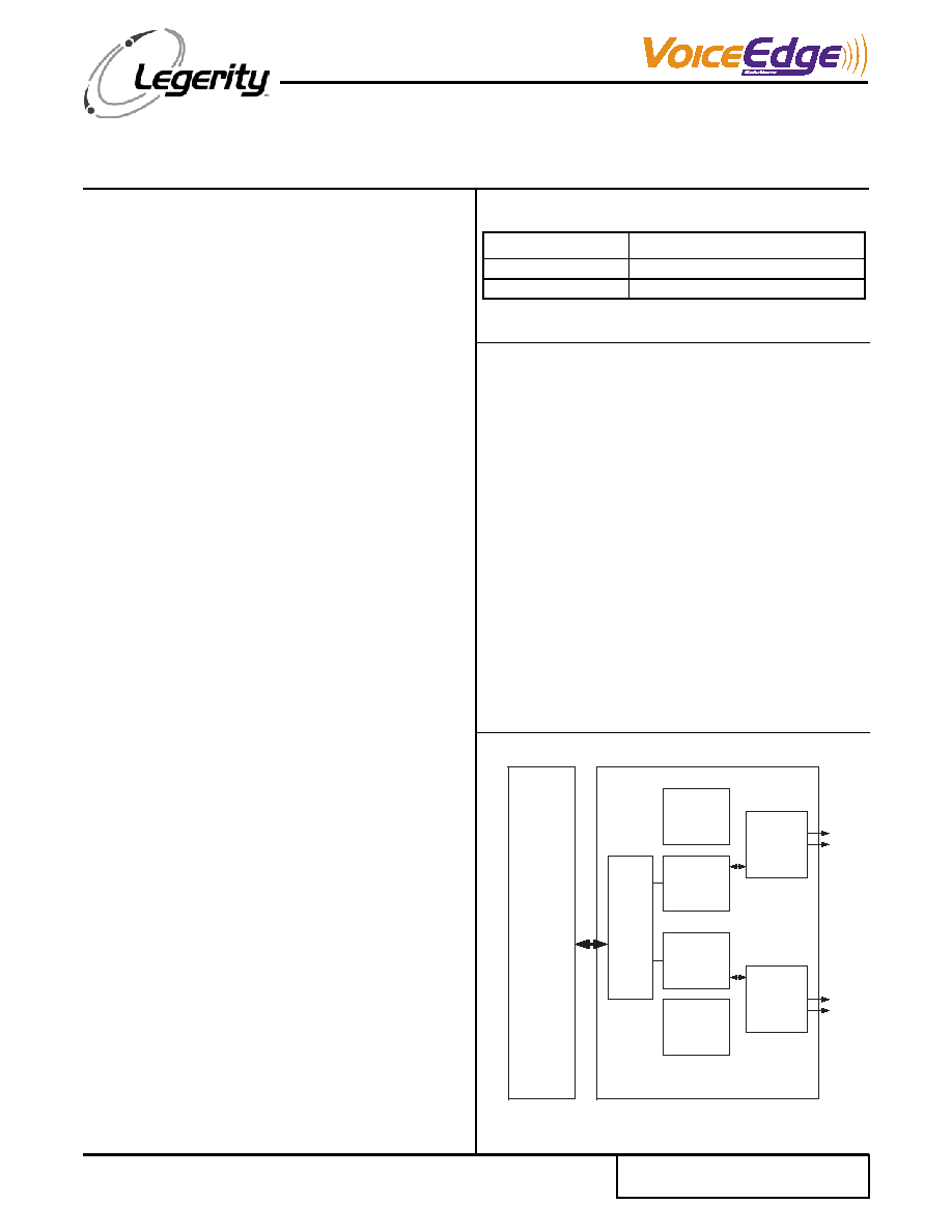
BLOCK DIAGRAM
2-wire to 4-wire
conversion
Switching Power
Supply
2-wire
Tip+Ring
Interface
Switching Power
Supply
2-wire to 4-wire
conversion
2-wire
Tip+Ring
Interface
Codec
Interface
Tip
Ring
Tip
Ring
Le78D11
Codec
Le77D11 SLIC

2
Le77D11 VE770 Series Data Sheet
TABLE OF CONTENTS
Applications . . . . . . . . . . . . . . . . . . . . . . . . . . . . . . . . . . . . . . . . . . . . . . . . . . . . . . . . . . . . . . . . . . . . . . .1
Features . . . . . . . . . . . . . . . . . . . . . . . . . . . . . . . . . . . . . . . . . . . . . . . . . . . . . . . . . . . . . . . . . . . . . . . . . .1
Related Literature . . . . . . . . . . . . . . . . . . . . . . . . . . . . . . . . . . . . . . . . . . . . . . . . . . . . . . . . . . . . . . . . . .1
Ordering Information. . . . . . . . . . . . . . . . . . . . . . . . . . . . . . . . . . . . . . . . . . . . . . . . . . . . . . . . . . . . . . . .1
Description. . . . . . . . . . . . . . . . . . . . . . . . . . . . . . . . . . . . . . . . . . . . . . . . . . . . . . . . . . . . . . . . . . . . . . . .1
Block Diagram . . . . . . . . . . . . . . . . . . . . . . . . . . . . . . . . . . . . . . . . . . . . . . . . . . . . . . . . . . . . . . . . . . . . .1
Product Description . . . . . . . . . . . . . . . . . . . . . . . . . . . . . . . . . . . . . . . . . . . . . . . . . . . . . . . . . . . . . . . .3
Block Descriptions . . . . . . . . . . . . . . . . . . . . . . . . . . . . . . . . . . . . . . . . . . . . . . . . . . . . . . . . . . . . . . . . .3
Two-Wire Interface . . . . . . . . . . . . . . . . . . . . . . . . . . . . . . . . . . . . . . . . . . . . . . . . . . . . . . . . . . . . .4
Switcher Controller . . . . . . . . . . . . . . . . . . . . . . . . . . . . . . . . . . . . . . . . . . . . . . . . . . . . . . . . . . . . .6
Signal Transmission . . . . . . . . . . . . . . . . . . . . . . . . . . . . . . . . . . . . . . . . . . . . . . . . . . . . . . . . . . . .7
Fault Detection. . . . . . . . . . . . . . . . . . . . . . . . . . . . . . . . . . . . . . . . . . . . . . . . . . . . . . . . . . . . . . . . .9
Signal Conditioning . . . . . . . . . . . . . . . . . . . . . . . . . . . . . . . . . . . . . . . . . . . . . . . . . . . . . . . . . . . . .9
Control Logic . . . . . . . . . . . . . . . . . . . . . . . . . . . . . . . . . . . . . . . . . . . . . . . . . . . . . . . . . . . . . . . . . .9
Connection Diagram . . . . . . . . . . . . . . . . . . . . . . . . . . . . . . . . . . . . . . . . . . . . . . . . . . . . . . . . . . . . . . .10
Pin Descriptions . . . . . . . . . . . . . . . . . . . . . . . . . . . . . . . . . . . . . . . . . . . . . . . . . . . . . . . . . . . . . . . . . .11
Absolute Maximum Ratings . . . . . . . . . . . . . . . . . . . . . . . . . . . . . . . . . . . . . . . . . . . . . . . . . . . . . . . . .12
Operating Ranges . . . . . . . . . . . . . . . . . . . . . . . . . . . . . . . . . . . . . . . . . . . . . . . . . . . . . . . . . . . . . . . . .12
Electrical Characteristics . . . . . . . . . . . . . . . . . . . . . . . . . . . . . . . . . . . . . . . . . . . . . . . . . . . . . . . . . . .13
Supply Currents and Power Dissipation . . . . . . . . . . . . . . . . . . . . . . . . . . . . . . . . . . . . . . . . . . . .13
Specifications . . . . . . . . . . . . . . . . . . . . . . . . . . . . . . . . . . . . . . . . . . . . . . . . . . . . . . . . . . . . . . . . . . . .14
System Specifications . . . . . . . . . . . . . . . . . . . . . . . . . . . . . . . . . . . . . . . . . . . . . . . . . . . . . . . . . .14
Device Specifications. . . . . . . . . . . . . . . . . . . . . . . . . . . . . . . . . . . . . . . . . . . . . . . . . . . . . . . . . . .14
Test Circuit. . . . . . . . . . . . . . . . . . . . . . . . . . . . . . . . . . . . . . . . . . . . . . . . . . . . . . . . . . . . . . . . . . . . . . .18
Single Channel Application Circuit . . . . . . . . . . . . . . . . . . . . . . . . . . . . . . . . . . . . . . . . . . . . . . . . . . .19
Application Circuit Parts List . . . . . . . . . . . . . . . . . . . . . . . . . . . . . . . . . . . . . . . . . . . . . . . . . . . . . . . .20
Physical Dimensions. . . . . . . . . . . . . . . . . . . . . . . . . . . . . . . . . . . . . . . . . . . . . . . . . . . . . . . . . . . . . . .21
44-Pin eTQFP . . . . . . . . . . . . . . . . . . . . . . . . . . . . . . . . . . . . . . . . . . . . . . . . . . . . . . . . . . . . . . . .21
Revision History . . . . . . . . . . . . . . . . . . . . . . . . . . . . . . . . . . . . . . . . . . . . . . . . . . . . . . . . . . . . . . . . . .22
Revision B1 to C1 . . . . . . . . . . . . . . . . . . . . . . . . . . . . . . . . . . . . . . . . . . . . . . . . . . . . . . . . . . . . .22
Revision C1 to D1 . . . . . . . . . . . . . . . . . . . . . . . . . . . . . . . . . . . . . . . . . . . . . . . . . . . . . . . . . . . . .22
Revision D1 to E1 . . . . . . . . . . . . . . . . . . . . . . . . . . . . . . . . . . . . . . . . . . . . . . . . . . . . . . . . . . . . .22
Revision E1 to F1 . . . . . . . . . . . . . . . . . . . . . . . . . . . . . . . . . . . . . . . . . . . . . . . . . . . . . . . . . . . . .22
Revision F1 to G1 . . . . . . . . . . . . . . . . . . . . . . . . . . . . . . . . . . . . . . . . . . . . . . . . . . . . . . . . . . . . .22

Le77D11 VE770 Series Data Sheet
3
PRODUCT DESCRIPTION
The dual channel Le77D11 VoSLIC device uses reliable, dielectrically isolated, fully complementary bipolar technology to
implement BORSCHT functions for short loop applications. Internal power dissipation is minimized by two independent line
voltage tracking, buck-boost switching regulators. Two power supplies are required: 3.3 V and a positive supply (V
SW
). A TTL-
level clock driven by the Le78D11 VoSLAC device is required for switcher operation. Six programmable states control loop
signaling, transmission, and ringing. The Le77D11 Dual VoSLIC device DC current limit (I
SC
) is programmable from 15 to 45 mA.
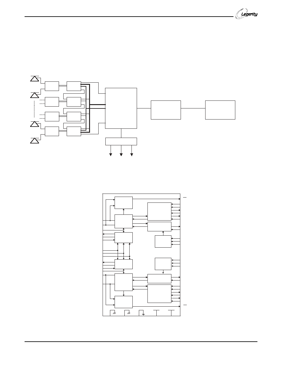
The following diagram demonstrates a typical application.
Figure 1. Typical Le77D11 VoSLICTM Device/Le78D11 VoSLACTM device
Application in an 8-Port Integrated Access Device in Customer Premises
BLOCK DESCRIPTIONS
Figure 2. Le77D11 VoSLICTM Device Block Diagram
DSLAM/
HEADEND
Loop/Cable
MODEM
WLL
Dout
Din
DSP
Network
Processor
Data Interfaces
Ethernet
USB HomePNA
Le78D11
Le78D11
Le78D11
Le78D11
Din
Dout
Le77D11
Le77D11
Le77D11
Le77D11
1
8
PCM I/F
DCLK/CS
RDC
2
IMT
2
VREG
2
SD
2
ILS
2
CHS
2
VSW
CHCLK
A
2
(TIP)
B
2
(RING)
C2
2
C1
2
C3
2
VIN
2
VOUT
2
CFILT
2
VHP
2
FSET
RDC
1
IMT
1
VREG
1
SD
1
ILS
1
CHS
1
A
1
(TIP)
B
1
(RING)
C2
1
C1
1
C3
1
Switcher
Controller
2-Wire
Interface
Signal
Transmission
Signal
Conditioning
Fault
Detection
Control
Logic
BGND
1
BGND
2
AGND
VREF
VCC
Switcher
Controller
2-Wire
Interface
Fault
Detection
Signal
Transmission
Signal
Conditioning
Control
Logic
F
2
LPF
2
NPRFILT
2
VIN
1
VOUT
1
CFILT
1
VHP
1
LPF
1
NPRFILT
1
F
1

4
Le77D11 VE770 Series Data Sheet
Two-Wire Interface
The two-wire interface block provides DC current and sends/receives voice signals to a telephone connected via the A
i
(Tip) and
B
i
(Ring) pins. The A
i
(Tip) and B
i
(Ring) pins are also used to send the ringing signal to the telephone. The Le77D11 VoSLIC
device can also be programmed in Disconnect state to place the A and B pins at high impedance with the Switching Regulator
disabled.
DC Feed
DC feed control in the Le78D11/Le77D11 chip set is implemented in the Le77D11 VoSLIC device. The current limit threshold
(I
LTH
) can be programmed via the MPI interface of the Le78D11 VoSLAC device. The current limit threshold (I
LTH
) can be
programmed up to 30 mA using the recommended R
DC
value.
Referring to
Figure 3
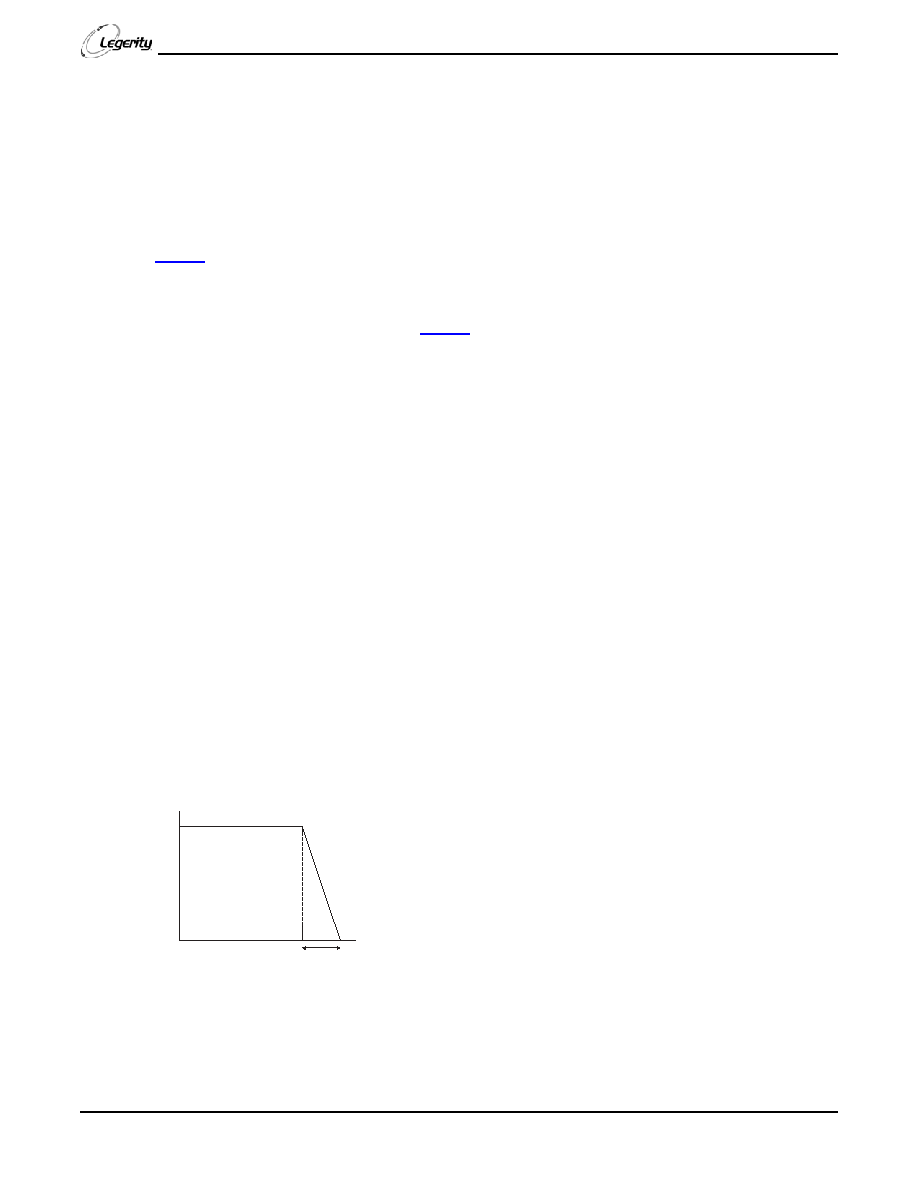
, the DC feed curve consists of two distinct regions. The first region is a flat anti-sat region that supplies a
constant Tip-Ring voltage (V
AB
open). The second region is a constant current region that begins when the loop current reaches
the programmed current limit threshold (I
LTH
). This region looks like a constant current source with 3.2 k
shunt resistor. The
short circuit current is nominally 14.4 mA greater than I
LTH
.
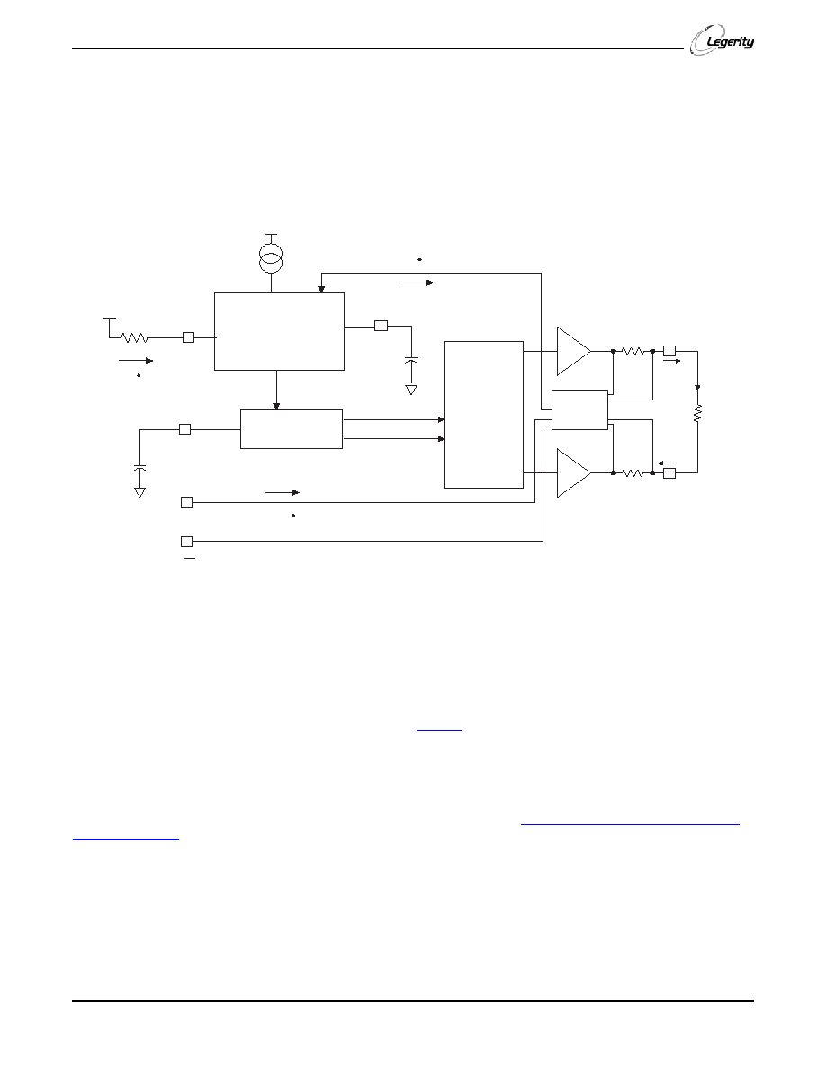
A block diagram of the DC feed control circuit is shown in
Figure 4
. In the anti-sat region, current source CS1 creates a constant
reference current, which is limited to sub-voice frequencies by C
LPFi
. This filtered current is then steered by the Polarity Control,
depending on whether the VoSLIC device mode is Standby, Normal Active, or Reverse Polarity. The steered current then takes
one of two paths to the Level Shift block, where it is used to set V
A
(TIP) and V
B
(RING). This voltage from the Level Shift block
is buffered by the output amplifiers and appears at A
i
(TIP) and B
i
(RING).
When I
LOOP
/500 becomes greater than I
LTH
/500, the difference is subtracted from CS1, and again filtered by C
LPFi
. This reduced
current causes a reduced DC feed voltage. In Standby and Normal Active, A
i
(TIP) is held constant, while B
i
(RING) is changed
to reduce the feed voltage. In Reverse Polarity, A
i
(TIP) and B
i
(RING) are swapped. When (I
LOOP
-I
LTH
)/500 = CS1], all of the
current from CS1 is subtracted, making the TIP-RING voltage = 0 V. This is the short circuit condition. At least 100
loop and
fuse resistance are required to ensure stability of the A
i
(TIP) and B
i
(RING) output amplifiers.
The capacitor C
LPFi
, in conjunction with an internal 25-k
resistor (not shown) is used to create a low pass filter for the DC feed
loop. This capacitor should nominally be 4.7 �F, setting a 1.4 Hz pole. The purpose of this filter is to separate the operation of the
DC feed from voice frequencies, preventing distortion and idle-channel noise.
Normal or Reverse Polarity is controlled by the Le78D11 VoSLAC device through the C3-1 state control pins. Some applications
require slew rate control of the transition between these feed states. The capacitor, C
NPRi
, may be used to increase the transition
time and create a quiet polarity change. In the Normal Active state, the NPRFILT
i
pin is driven up to V
CC
.
When Reverse Polarity is selected, C
NPRi
is discharged by current I
NPR
, and the transition time is:
In the Reverse Polarity state, the NPRFILT
i
pin is discharged near ground. When Normal Active is selected, C
NPRi
is charged by
current I
NPR
, and the transition time is:
A 100-nF capacitor provides a nominal Normal Active to Reverse Polarity transition time of about 5 ms and a Reverse Polarity
to Normal Active transition time of 3 ms.
Figure 3. DC Feed Curve
t
V
CC
V
�
REF
(
) C
NPRi
�
I
NPR
---------------------------------------------------------
=
t
V
REF
C
NPRi
�
I
NPR
-----------------------------------
=
I
LOOP
I
LTH
V
AB
open
(48 V)
V
AB
0
14.4 mA
I
SC
I
SC
I
LTH
14.4mA
+
=
I
LTH
V
DC
R
DC
K
DC
----------------------
V
DC
40
-----------
=
=

Le77D11 VE770 Series Data Sheet
5
Notes:
1.
V
DC
is programmable via the Le78D11 VoSLAC device. (V
DC
= 0.00 V to 1.20 V relative to V
REF
.)
2.
V
REF
= 1.4 V nominal.
3.
K
DC
= Le77D11 VoSLIC device DC current gain.
.
4.
R
DC
= external resistor 20 k
nominal.
5.
V
AB
= V
Ai
� V
Bi
Tip-Ring differential voltage.
6.
I
SC
= Loop short circuit current limit.
7.
I
LTH
= Loop current limit threshold. I
LTH
should be programmed to 15 mA or less when in the Standby state.
8.
These are nominal values for DC feed curve. See the "Device Specifications" table for tolerance values.
Figure 4. DC Feed Block Diagram, Active and Standby Modes
Note:
* denotes external components
Ringing
Ringing is accomplished by placing the Le77D11 VoSLIC device into the Ringing state via the Le78D11 VoSLAC device's MPI
interface. Placing the Le77D11 VoSLIC device into the ringing state automatically enables signal generator A in the Le78D11
VoSLAC device which puts the ringing signal on the receive signal path (pin VIN). (For information on programming the Le78D11
VoSLAC device's signal generators, please refer to the Le77D11 /Le78D11 Chip Set User's Guide, document ID# 080716). When
the Le77D11 VoSLIC device is in the ringing state, the gain from the input pin, VIN, to the output is K
R
, the ringing voltage gain.
The output waveform is a quasi-balanced waveform, as shown in
Figure 5
. On the positive half cycle of the input waveform, when
(V
IN
� V
REF
) is positive, V
AB
is positive with V
A(TIP)
near �4 V and V
B(RING)
brought negative. When (V
IN
� V
REF
) is negative,
V
B(RING)
is held near �4 V and V
A(TIP)
is brought more negative.
The waveform can be either sinusoidal or trapezoidal under the
control of the Le78D11 VoSLAC device.
To provide 90-V ringing capability, the application of a PNP bipolar switching transistor is used. For the reference schematic,
Zetex part FZT955 in a SOT-223 package is used. Its V
CEO
rating is 140 V. Due to the switching efficiency and overhead voltage,
one can achieve 90 Vpk sinusoidal ringing with a 5 REN load with V
SW
= 12 V. See
Figure 6, Switching Power Supply Block
Diagram, on page 7
for external filters recommended for a 90-V peak ringing application.
K
DC
I
IMT
I
LOOP
---------------
=
R
DC
*
VDC SLAC
C
NPRi
*
LPF
i
A
i
(TIP)
B
i
(RING)
RDC
i
NPRFILT
i
C
LPFi
*
Current Mirrors
Polarity Control
Sum/
Sense/
Fault
Level Shift
CS1
VCC
R
S
R
S
IMT
i
I
LOOP
K
DC
R
L
I
B
I
LOOP
K
DC
I
LTH
K
DC
I
LOOP
I
A
F
i
