TM
Document ID#: 080152 Date:
Nov 15, 2006
Rev:
N
Version: 2
Distribution:
Public Document
Le79R79
Ringing Subscriber Line Interface Circuit
VE580 Series
APPLICATIONS
Ideal for short-loop applications
Ideal for ISDN-TA and fixed radio access applications
Integrated Access Devices (IADs)
Network Interface Units (NIUs)
Cable Modems
DSL Modems
Set Top / House Side Boxes
Intelligent PBX
Pain Gain
FXS Cards
Voice over ISDN or T1/E1
Smart Residential Gateways
WLL, APON, FITL, NGN, and all other short-loop CPE/
Enterprise telephony applications
FEATURES
Through trapezoidal ringing
On-chip ring-trip detector
Low standby state power
Battery operation:
-- V
BAT1
: �40.5 to �75 V
-- V
BAT2
: �19 V to V
BAT1
On-chip battery switching and feed selection
On-hook transmission
Two-wire impedance set by single external impedance
Programmable constant-current feed
Programmable Open Circuit voltage
Programmable loop-detect threshold
Current gain = 1000
Ground-key detector
Polarity reversal option available
Internal V
EE
regulator (no external �5 V power supply
required)
RELATED LITERATURE
080917 Ve790 Series RSLIC Device Product Brief
080158 Le79R70/79/100/101 Technical Overview
080914 Le79R79 RSLIC Device User's Guide
080810 Le71HR0021 Reference Design User's Guide
080255 Le71HE0040J Evaluation Board User's Guide
080458 Le79R100/101 v. Le79R79 Comparison Brief
080753 Le58QL02/021/031 QLSLACTM Data Sheet
ORDERING INFORMATION
-1: 52 dB Longitudinal Balance, Polarity Reversal
-2: 63 dB Longitudinal Balance, Polarity Reversal
-3: 52 dB Longitudinal Balance, No Polarity Reversal
1.
Legerity reserves the right to fulfill all orders for this device with
parts marked with the "Am" part number prefix, until such time as
all inventory bearing this mark has been depleted. It should be
noted that parts marked with either the "Am" or the "Le" part
number prefix are equivalent devices in terms of form, fit, and
function.
2.
Due to size constraints, QFN devices are marked by omitting the
"Le" prefix and the performance grade dash character. For
example, Le79R79-1FQC is marked 79R791FQC.
3.
The green package meets RoHS Directive 2002/95/EC of the
European Council to minimize the environmental impact of
electrical equipment.
4.
For delivery using a tape and reel packing system, add a "T" suffix
to the OPN (Ordering Part Number) when placing an order.
Device
1
Package Type
2, 3
Packing
4
Le79R79-1DJC
32-pin PLCC
(Green package)
Tube
Le79R79-2DJC
Le79R79-3DJC
Le79R79-1FQC
32-pin QFN
(Green package)
Tray
Le79R79-2FQC
DESCRIPTION
The Le79R79 Ringing SLIC device is a bipolar monolithic SLIC
that offers on-chip ringing. Designers can achieve significant
cost reductions at the system level for short-loop applications
by integrating the ringing function on chip. Examples of such
applications would be ISDN terminal adaptors, fiber-in-the-
loop, radio-in-the-loop, hybrid fiber/coax and video telephony
(home-side) boxes. The Le79R79 Ringing SLIC device can
provide sufficient voltage to meet the stringent LSSGR five-
ringer equivalent specification. Using a CMOS-compatible
input waveform and wave shaping R-C network, the Le79R79
Ringing SLIC device can provide trapezoidal wave ringing to
meet various design requirements.
See the
Le79R79 Block Diagram, on page 3
.

2
Le79R79 VE580 Series Data Sheet
TABLE OF CONTENTS
Applications . . . . . . . . . . . . . . . . . . . . . . . . . . . . . . . . . . . . . . . . . . . . . . . . . . . . . . . . . . . . . . . . . . . . . . .1
Features . . . . . . . . . . . . . . . . . . . . . . . . . . . . . . . . . . . . . . . . . . . . . . . . . . . . . . . . . . . . . . . . . . . . . . . . . .1
Related Literature . . . . . . . . . . . . . . . . . . . . . . . . . . . . . . . . . . . . . . . . . . . . . . . . . . . . . . . . . . . . . . . . . .1
Ordering Information. . . . . . . . . . . . . . . . . . . . . . . . . . . . . . . . . . . . . . . . . . . . . . . . . . . . . . . . . . . . . . . .1
Description. . . . . . . . . . . . . . . . . . . . . . . . . . . . . . . . . . . . . . . . . . . . . . . . . . . . . . . . . . . . . . . . . . . . . . . .1
Product Description . . . . . . . . . . . . . . . . . . . . . . . . . . . . . . . . . . . . . . . . . . . . . . . . . . . . . . . . . . . . . . . .3
Connection Diagrams . . . . . . . . . . . . . . . . . . . . . . . . . . . . . . . . . . . . . . . . . . . . . . . . . . . . . . . . . . . . . .4
Electrical Characteristics . . . . . . . . . . . . . . . . . . . . . . . . . . . . . . . . . . . . . . . . . . . . . . . . . . . . . . . . . . . .6
Absolute Maximum Ratings . . . . . . . . . . . . . . . . . . . . . . . . . . . . . . . . . . . . . . . . . . . . . . . . . . . . . . .6
Operating Ranges . . . . . . . . . . . . . . . . . . . . . . . . . . . . . . . . . . . . . . . . . . . . . . . . . . . . . . . . . . . . . . . . . .7
Specifications . . . . . . . . . . . . . . . . . . . . . . . . . . . . . . . . . . . . . . . . . . . . . . . . . . . . . . . . . . . . . . . . . . . . .7
Transmission Performance . . . . . . . . . . . . . . . . . . . . . . . . . . . . . . . . . . . . . . . . . . . . . . . . . . . . . . .7
Longitudinal Performance . . . . . . . . . . . . . . . . . . . . . . . . . . . . . . . . . . . . . . . . . . . . . . . . . . . . . . . .8
Idle Channel Noise . . . . . . . . . . . . . . . . . . . . . . . . . . . . . . . . . . . . . . . . . . . . . . . . . . . . . . . . . . . . .8
Insertion Loss and Four-to-Four-Wire Balance Return Signal . . . . . . . . . . . . . . . . . . . . . . . . . . . . .8
Line Characteristics . . . . . . . . . . . . . . . . . . . . . . . . . . . . . . . . . . . . . . . . . . . . . . . . . . . . . . . . . . . . .9
Power Supply Rejection Ratio . . . . . . . . . . . . . . . . . . . . . . . . . . . . . . . . . . . . . . . . . . . . . . . . . . . . .9
Power Dissipation . . . . . . . . . . . . . . . . . . . . . . . . . . . . . . . . . . . . . . . . . . . . . . . . . . . . . . . . . . . . . .9
Supply Currents . . . . . . . . . . . . . . . . . . . . . . . . . . . . . . . . . . . . . . . . . . . . . . . . . . . . . . . . . . . . . . .10
Logic Inputs . . . . . . . . . . . . . . . . . . . . . . . . . . . . . . . . . . . . . . . . . . . . . . . . . . . . . . . . . . . . . . . . . .10
Logic Output . . . . . . . . . . . . . . . . . . . . . . . . . . . . . . . . . . . . . . . . . . . . . . . . . . . . . . . . . . . . . . . . .10
Ring-Trip Detector Input . . . . . . . . . . . . . . . . . . . . . . . . . . . . . . . . . . . . . . . . . . . . . . . . . . . . . . . .10
Ring Signal . . . . . . . . . . . . . . . . . . . . . . . . . . . . . . . . . . . . . . . . . . . . . . . . . . . . . . . . . . . . . . . . . .10
Ground-Key Detector Thresholds . . . . . . . . . . . . . . . . . . . . . . . . . . . . . . . . . . . . . . . . . . . . . . . . .10
Loop Detector . . . . . . . . . . . . . . . . . . . . . . . . . . . . . . . . . . . . . . . . . . . . . . . . . . . . . . . . . . . . . . . .11
Relay Driver Output . . . . . . . . . . . . . . . . . . . . . . . . . . . . . . . . . . . . . . . . . . . . . . . . . . . . . . . . . . . .11
Relay Driver Schematic. . . . . . . . . . . . . . . . . . . . . . . . . . . . . . . . . . . . . . . . . . . . . . . . . . . . . . . . . . . . .11
SLIC Device Decoding . . . . . . . . . . . . . . . . . . . . . . . . . . . . . . . . . . . . . . . . . . . . . . . . . . . . . . . . .12
User-Programmable Components . . . . . . . . . . . . . . . . . . . . . . . . . . . . . . . . . . . . . . . . . . . . . . . . .13
DC Feed Characteristics . . . . . . . . . . . . . . . . . . . . . . . . . . . . . . . . . . . . . . . . . . . . . . . . . . . . . . . . . . . .14
Ring-Trip Components . . . . . . . . . . . . . . . . . . . . . . . . . . . . . . . . . . . . . . . . . . . . . . . . . . . . . . . . . . . . .15
Test Circuits. . . . . . . . . . . . . . . . . . . . . . . . . . . . . . . . . . . . . . . . . . . . . . . . . . . . . . . . . . . . . . . . . . . . . .16
Le79R79 Test Circuit . . . . . . . . . . . . . . . . . . . . . . . . . . . . . . . . . . . . . . . . . . . . . . . . . . . . . . . . . . . . . . .19
Application Circuit. . . . . . . . . . . . . . . . . . . . . . . . . . . . . . . . . . . . . . . . . . . . . . . . . . . . . . . . . . . . . . . . .20
Physical Dimensions. . . . . . . . . . . . . . . . . . . . . . . . . . . . . . . . . . . . . . . . . . . . . . . . . . . . . . . . . . . . . . .21
32-pin PLCC . . . . . . . . . . . . . . . . . . . . . . . . . . . . . . . . . . . . . . . . . . . . . . . . . . . . . . . . . . . . . . . . .21
32-pin QFN . . . . . . . . . . . . . . . . . . . . . . . . . . . . . . . . . . . . . . . . . . . . . . . . . . . . . . . . . . . . . . . . . .22
Revision History . . . . . . . . . . . . . . . . . . . . . . . . . . . . . . . . . . . . . . . . . . . . . . . . . . . . . . . . . . . . . . . . . .23
Revision B to C . . . . . . . . . . . . . . . . . . . . . . . . . . . . . . . . . . . . . . . . . . . . . . . . . . . . . . . . . . . . . . .23
Revision C to D . . . . . . . . . . . . . . . . . . . . . . . . . . . . . . . . . . . . . . . . . . . . . . . . . . . . . . . . . . . . . . .23
Revision D to E . . . . . . . . . . . . . . . . . . . . . . . . . . . . . . . . . . . . . . . . . . . . . . . . . . . . . . . . . . . . . . .23
Revision E to F . . . . . . . . . . . . . . . . . . . . . . . . . . . . . . . . . . . . . . . . . . . . . . . . . . . . . . . . . . . . . . .23
Revision F to G . . . . . . . . . . . . . . . . . . . . . . . . . . . . . . . . . . . . . . . . . . . . . . . . . . . . . . . . . . . . . . .23
Revision G to H . . . . . . . . . . . . . . . . . . . . . . . . . . . . . . . . . . . . . . . . . . . . . . . . . . . . . . . . . . . . . . .23
Revision H to I . . . . . . . . . . . . . . . . . . . . . . . . . . . . . . . . . . . . . . . . . . . . . . . . . . . . . . . . . . . . . . . .23
Revision I to J1 . . . . . . . . . . . . . . . . . . . . . . . . . . . . . . . . . . . . . . . . . . . . . . . . . . . . . . . . . . . . . . .23
Revision J1 to K1 . . . . . . . . . . . . . . . . . . . . . . . . . . . . . . . . . . . . . . . . . . . . . . . . . . . . . . . . . . . . . .23
Revision K1 to L1. . . . . . . . . . . . . . . . . . . . . . . . . . . . . . . . . . . . . . . . . . . . . . . . . . . . . . . . . . . . . .23
Revision L1 to M1 . . . . . . . . . . . . . . . . . . . . . . . . . . . . . . . . . . . . . . . . . . . . . . . . . . . . . . . . . . . . .23
Revision M1 to N1 . . . . . . . . . . . . . . . . . . . . . . . . . . . . . . . . . . . . . . . . . . . . . . . . . . . . . . . . . . . . .24
Revision N1 to N2 . . . . . . . . . . . . . . . . . . . . . . . . . . . . . . . . . . . . . . . . . . . . . . . . . . . . . . . . . . . . .24
Le79R79 VE580 Series Data Sheet
3
PRODUCT DESCRIPTION
The Legerity family of subscriber line interface circuit (SLIC) products provide the telephone interface functions required
throughout the worldwide market. Legerity SLIC devices address all major telephony markets including central office (CO),
private branch exchange (PBX), digital loop carrier (DLC), fiber-in-the-loop (FITL), radio-in-the-loop (RITL), hybrid fiber coax
(HFC), and video telephony applications.
The Legerity SLIC devices offer support of BORSHT (battery feed, overvoltage protection, ringing, supervision, hybrid, and test)
functions with features including current limiting, on-hook transmission, polarity reversal, Tip Open, and loop-current detection.
These features allow reduction of linecard cost by minimizing component count, conserving board space, and supporting
automated manufacturing.
The Legerity SLIC devices provide the two- to four-wire hybrid function, DC-loop feed, and two-wire supervision. Two-wire
termination is programmed by a scaled impedance network. Transhybrid balance can be achieved with an external balance
circuit or simply programmed using a companion Legerity codec device, the Am79C02/03/031 DSLACTM device, the Am79Q02/
021/03 Programmable Quad SLAC (QSLACTM) device, or the Am79Q5457/4457 Nonprogrammable QSLAC device.
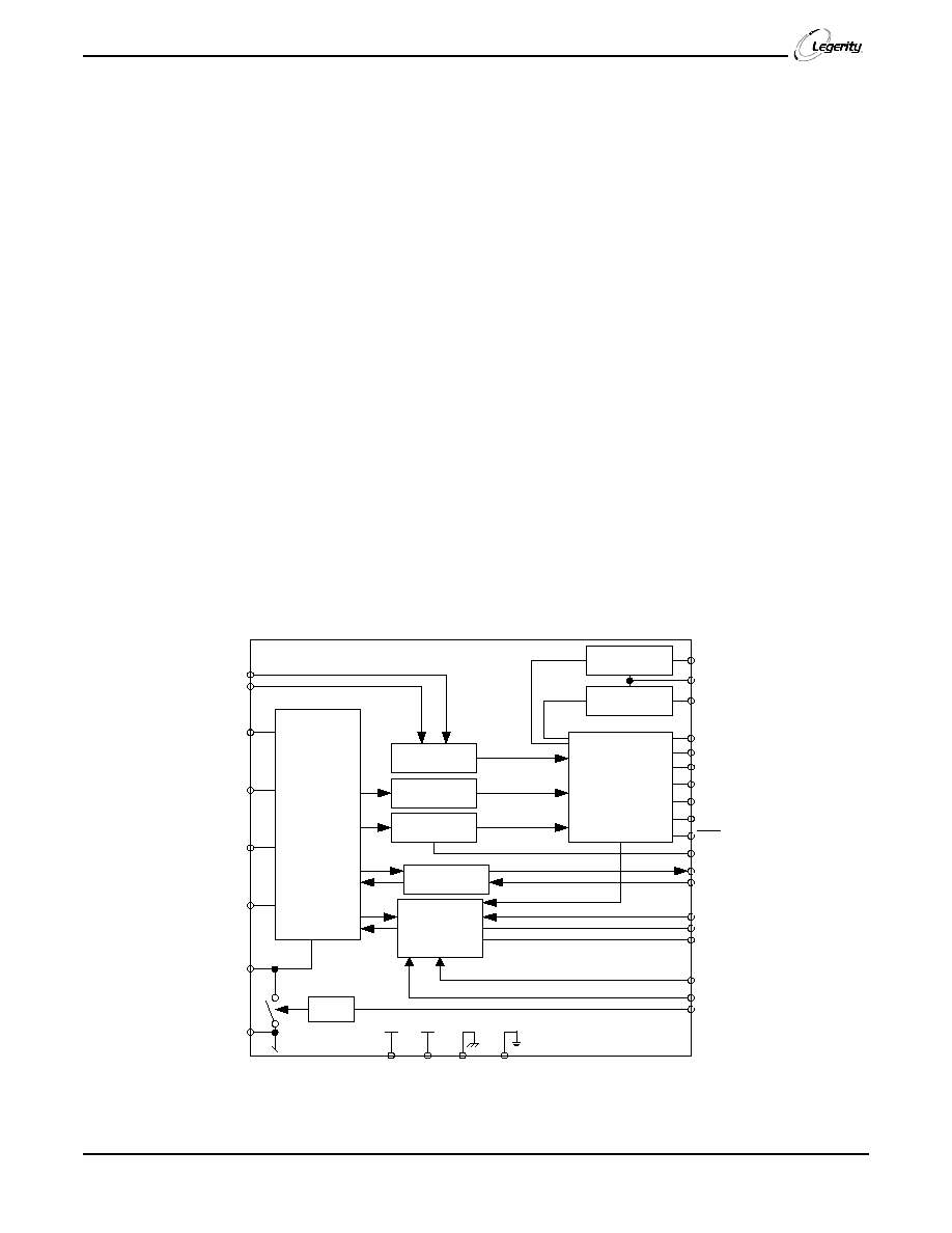
The Le79R79 Ringing SLIC device is a bipolar monolithic SLIC that offers on-chip ringing. Now designers can achieve significant
cost reductions at the system level for short-loop applications by integrating the ringing function on chip. Examples of such
applications would be ISDN terminal adaptors, fiber-in-the-loop, radio-in-the-loop, hybrid fiber/coax and video telephony (home-
side) boxes. The Le79R79 Ringing SLIC can provide sufficient voltage to meet the stringent LSSGR five-ringer equivalent
specification. Using a CMOS-compatible input waveform and wave shaping R-C network, the Le79R79 Ringing SLIC can provide
trapezoidal wave ringing to meet various design requirements.
In order to further enhance the suitability of this device in short-loop, distributed switching applications, Legerity has maximized
power savings by incorporating battery switching on chip. The Le79R79 Ringing SLIC device switches between two battery
supplies such that in the off-hook (active) state, a low battery is used to save power. In order to meet the Open Circuit voltage
requirements of fax machines and maintenance termination units (MTU), the SLIC device automatically switches to a higher
voltage in the On-hook (Standby) state.
Like all of the Legerity SLIC devices, the Le79R79 Ringing SLIC device supports on-hook transmission, ring-trip detection,
programmable loop-detect threshold, and is available with on-chip polarity reversal. The Le79R79 Ringing SLIC device is a
programmable constant-current feed device with two on-chip relay drivers to operate external relays. Several performance
grades are available to meet both CCITT and LSSGR requirements, including various longitudinal balance options.
Figure 1. Le79R79 Block Diagram
Two-Wire
Interface
Ring-Trip
Detector
Ground-Key
Detector
Off-Hook
Detector
Signal
Transmission
Power-Feed
Controller
Switch
Driver
RTRIP1
RTRIP2
A(TIP)
HPA
HPB
B(RING)
VBAT2
VBAT1
VCC VNEG BGND
AGND/DGND
Relay Driver
Relay Driver
Input Decoder
and Control
RYOUT2
RYE
RYOUT1
D1
D2
C1
C2
C3
E1
RD
VTX
RSN
RINGIN
RDC
RDCR
RSGL
RSGH
DET
B2EN
4
Le79R79 VE580 Series Data Sheet
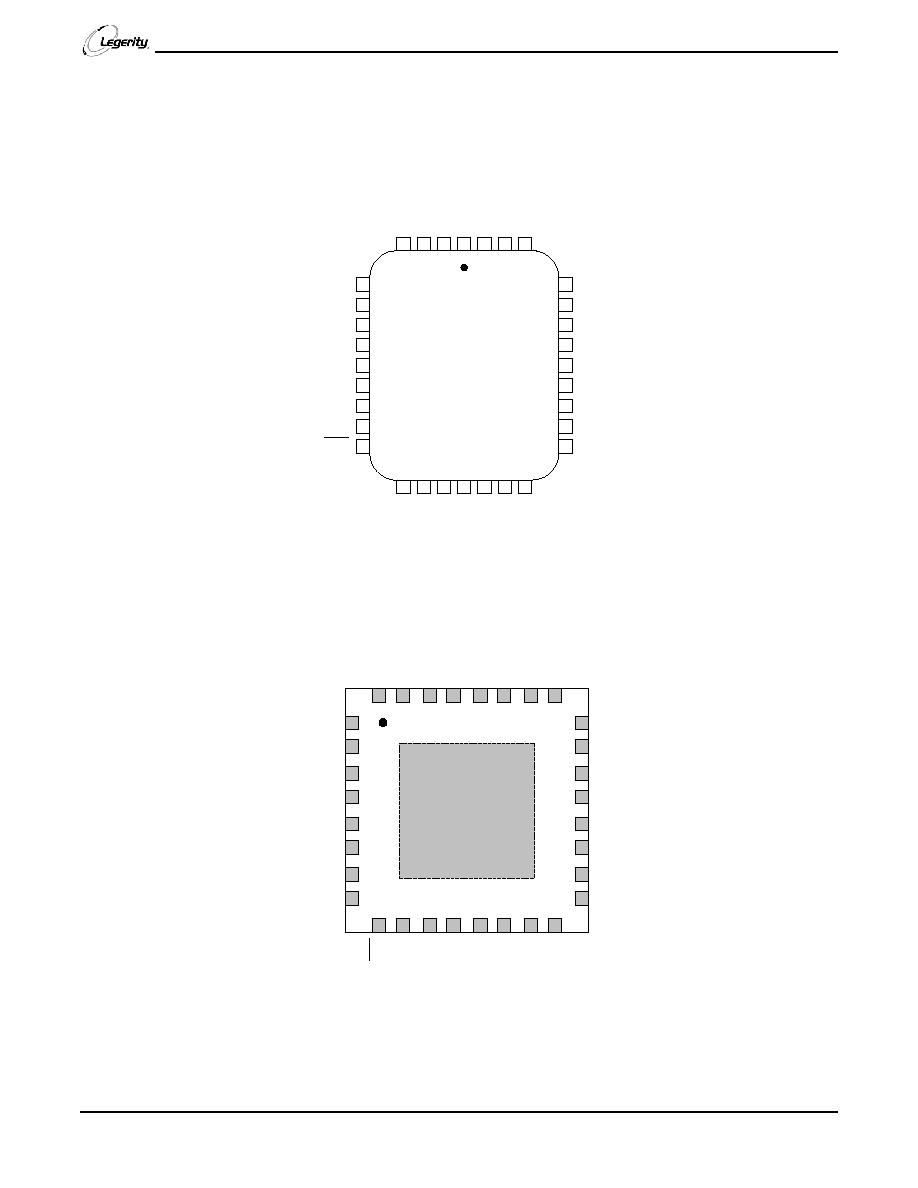
CONNECTION DIAGRAMS
Note:
1.
Pin 1 is marked for orientation.
2.
NC = No connect.
3.
The thermally enhanced QFN package features an exposed pad on the underside which must be electrically tied to VBAT1.
RYOUT2
VCC
VBAT2
BGND
B(RING)
A(TIP)
RD
4
3
2
1
32
31
30
29
28
27
26
25
24
23
22
21
5
6
7
8
9
10
11
12
13
14
15
16
17
18
19
20
C1
D2
NC
RSGH
RSGL
RDC
AGND/DGND
RTRIP1
RTRIP2
HPB
HPA
RINGIN
RDCR
VTX
VNEG
RSN
DET
VBAT1
RYE
RYOUT1
32-pin PLCC
B2EN
D1
E1
C3
C2
EXPOSED PAD
32-pin QFN
1
21
20
19
18
17
22
23
24
2
3
4
5
6
7
8
10
9
12
11
14
13
16
15
32
31
30
29
28
27
26
25
Top View
RSN
VNEG
VTX
RDCR
RINGIN
HPA
HPB
RTRIP2
E1
C3
C2
RYE
RYOUT1
B2EN
VBAT1
D1
RTRIP1
AX
RD
BX
VBAT2
BGND
VCC
RYOUT2
DET
C1
D2
AGND
RSGL
RDC
NC
RSGH

Le79R79 VE580 Series Data Sheet
5
PIN DESCRIPTIONS
Pin Names
Type
Description
AGND/DGND
Ground
Analog and digital ground
A(TIP)
Output
Output of A(TIP) power amplifier
B2EN
Input
V
BAT2
Enable. Logic Low enables operation from V
BAT2
. Logic High enables operation from V
BAT1
. TTL
compatible.
BGND
Ground
Battery (power) ground
B(RING)
Output
Output of B(RING) power amplifier
C3�C1
Input
Decoder. SLIC control pins. C3 is MSB and C1 is LSB. TTL compatible.
D1
Input
Relay1 Control. TTL compatible. Logic Low activates the Relay1 relay driver.
D2
Input
Relay2 Control. (Option) TTL compatible. Logic Low activates the Relay2 relay driver.
DET
Output
Hook switch detector. When enabled, a logic Low indicates that the selected detector is tripped. The logic
inputs C3�C1 and E1 select the detector. The output is open collector with a built-in 15 k
pull-up resistor.
E1
Input
Ground-Key Enable. (Option) A logic High selects the off-hook detector. A logic Low selects the ground-
key detector. TTL compatible.
HPA
Capacitor
High-Pass Filter. A(TIP) side of high-pass filter capacitor.
HPB
Capacitor
High-Pass Filter. B(RING) side of high-pass filter capacitor.
NC
--
Not internally connected.
RD
Resistor
Detect Resistor. Detector threshold set and filter pin.
RDC
Output
DC Feed Resistor. Connection point for the DC-feed current programming network. The other end of the
network connects to the receiver summing node (RSN). The sign of V
RDC
is negative for normal polarity
and positive for reverse polarity.
RDCR
--
Connection point for feedback during ringing.
RINGIN
Input
Ring Signal. Pin for ring signal input. Square-wave shaped by external RC filter. Requires 50% duty cycle.
CMOS-compatible input.
RSGH
Input
Saturation Guard High. Pin for resistor to adjust Open Circuit voltage when operating from V
BAT1
.
RSGL
Input
Saturation Guard Low. Pin for resistor to adjust the anti-saturation cut-in voltage when operating from
both V
BAT1 and
V
BAT2
.
RSN
Input
Receive Summing Node. The metallic current (both AC and DC) between A(TIP) and B(RING) is equal
to 1000 x the current into this pin. The networks that program receive gain, two-wire impedance, and feed
resistance all connect to this node.
RTRIP1
Input
Ring-Trip Detector. Ring-trip detector threshold set and filter pin.
RTRIP2
Input
Ring-Trip Detector. Ring-trip detector threshold offset (switch to V
BAT1
). For power conservation in any
nonringing state, this switch is open.
RYE
Output
Common Emitter of RYOUT1/RYOUT2. Emitter output of RYOUT1 and RYOUT2. Normally connected to
relay ground.
RYOUT1
Output
Relay/Switch Driver. Open collector driver with emitter internally connected to RYE.
RYOUT2
Output
Relay/Switch Driver. (Option) Open collector driver with emitter internally connected to RYE.
VBAT1
Battery
Battery supply and connection to substrate.
VBAT2
Battery
Power supply to output amplifiers. Connect to off-hook battery through a diode.
VCC
Power
Positive analog power supply
VNEG
Power
Negative analog power supply. This pin is the return for the internal V
EE
regulator.
VTX
Output
Transmit Audio. This output is a 0.5066 gain version of the A(TIP) and B(RING) metallic AC voltage. VTX
also sources the two-wire input impedance programming network.