FEATURES
DIRECT REPLACEMENT FOR INTERSIL 2N4351
HIGH DRAIN CURRENT
I
D
= 100mA
HIGH GAIN
g
fs
= 1000µS
ABSOLUTE MAXIMUM RATINGS
1
@ 25 ∞C (unless otherwise stated)
Maximum Temperatures
Storage Temperature
-65 to +200 ∞C
Operating Junction Temperature
-55 to +150 ∞C
Maximum Power Dissipation
Continuous Power Dissipation
375mW
Maximum Current
Drain to Source
100mA
Maximum Voltages
Drain to Body
25V
Drain to Source
25V
Peak Gate to Source
2
±125V
ELECTRICAL CHARACTERISTICS @ 25 ∞C (unless otherwise stated) (V
SB
= 0V unless otherwise stated)
SYMBOL
CHARACTERISTIC
MIN TYP MAX UNITS
CONDITIONS
BV
DSS
Drain to Source Breakdown Voltage
25
I
D
= 10µA, V
GS
= 0V
V
DS(on)
Drain to Source "On" Voltage
1
I
D
= 2mA, V
GS
= 10V
V
GS(th)
Gate to Source Threshold Voltage
1
5
V
V
DS
= 10V, I
D
= 10µA
I
GSS
Gate
Leakage
Current
10
pA
V
GS
= ±30V, V
DS
= 0V
I
DSS
Drain Leakage Current "Off"
10
nA
V
DS
= 10V, V
GS
= 0V
I
D(on)
Drain Current "On"
3
mA
V
GS
= 10V, V
DS
= 10V
g
fs
Forward
Transconductance
1000
µS
V
DS
= 10V, I
D
= 2mA, f = 1MHz
r
DS(on)
Drain to Source "On" Resistance
300
V
GS
= 10V, I
D
= 0A, f = 1kHz
C
rss
Reverse Transfer Capacitance
1.3
V
DS
= 0V, V
GS
= 0V, f = 140kHz
C
iss
Input
Capacitance
5.0
V
DS
= 10V, V
GS
= 0V, f = 140kHz
C
db
Drain to Body Capacitance
5.0
pF
V
DB
= 10V, f = 140kHz
* Body tied to Case.
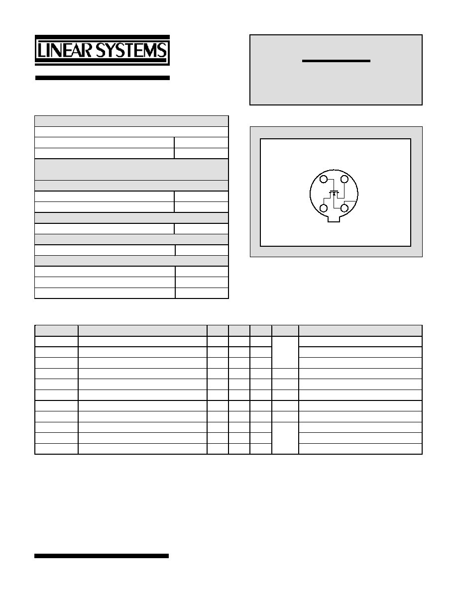
G
S
D
C
2
1
4
3
BOTTOM VIEW
TO-72
Linear Integrated Systems
2N4351
N-CHANNEL MOSFET
ENHANCEMENT MODE
Linear Integrated Systems
∑ 4042 Clipper Court ∑ Fremont, CA 94538 ∑ Tel: 510 490-9160 ∑ Fax: 510 353-0261
Linear Integrated Systems
∑ 4042 Clipper Court ∑ Fremont, CA 94538 ∑ Tel: 510 490-9160 ∑ Fax: 510 353-0261
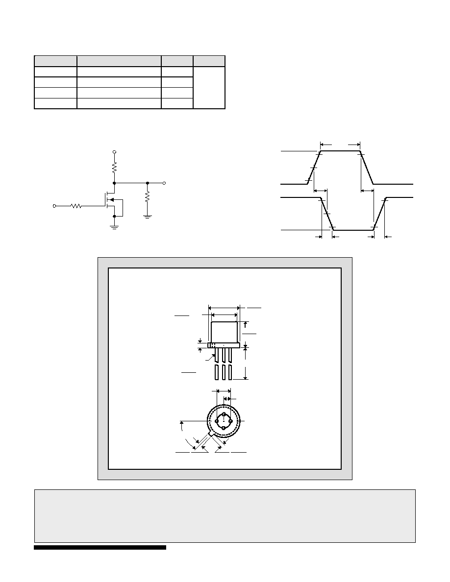
SWITCHING CHARACTERISTICS
SYMBOL
CHARACTERISTIC
MAX
UNITS
t
d(on)
Turn On Delay Time
45
t
r
Turn On Rise Time
65
t
d(off)
Turn Off Delay Time
60
t
f
Turn Off Fall Time
100
ns
TO-72
Four Lead
0.230
0.209
DIA.
DIA.
0.195
0.175
0.030
MAX.
0.500 MIN.
0.150
0.115
0.019
0.016
DIA.
4 LEADS
2
1
3
0.046
0.036
45∞
0.048
0.028
0.100
0.050
4
4.5k
51
8.21k
V
DD
V
IN
V
OUT
SET
V
DS
= 10V
SWITCHING TEST CIRCUIT
TIMING WAVEFORMS
d(on)
90%
50%
10%
t
r
t
f
t
d(off)
0 V
+10 V
V
DS
t
90%
50%
10%
0 V
+10 V
V
IN
10 µs
t
r
= t
f
< 2 ns
Duty Cycle 2%
1.
Absolute maximum ratings are limiting values above which serviceability may be impaired.
2.
Device must not be tested at ±125V more than once or longer than 300ms.
Information furnished by Linear Integrated Systems is believed to be accurate and reliable. However, no responsibility is assumed for its
use; nor for any infringement of patents or other rights of third parties which may result from its use. No license is granted by implicatio
otherwise under any patent or patent rights of Linear Integrated Systems.
n or