1/101
www.dynexsemi.com
54HSC/T Series
The CMOS/SOS HSC/T Series offer the combined benefits
of low power, high speed CMOS with the inherent latch up
immunity, Single Event Upset (SEU) immunity and the high
level of radiation hardness of Silicon on Sapphire technology.
The 54HSC/T Series of circuits are pin for pin compatible with
the 54LS series range.
HSC and HST devices have CMOS and TTL compatible
inputs/outputs respectively.
FEATURES
s
Radiation Hard to 1MRad (Si)
s
High SEU Immunity, Latch Up Free
s
Low Power CMOS/SOS Technology
s
Plug In Replacement for 54/74LS, HC and HCT
s
Dual In Line or Flatpack Packages
Adders
54HSC/T283
4-bit binary full adders with fast carry
Counters
54HSC/T161
4-bit synchronous binary counter
54HSC/T163
Synchronous 4-bit counter
54HSC/T191
Synchronous 4-bit counter
Decoders/Demultiplexers
54HSC/T138
3-line to 8-line decoder/multiplexer
54HSC/T139
Dual 2 to 4 decoders/multiplexers
54HSC/T148
8-line to 3-line octal priority encoders
54HSC/T151
1 of 8 data selectors/multiplexers
54HSC/T154
4 to 16-line decoders/demultiplexers
54HSC/T157
Quad 2-line to 1-line data selectors/multiplexers
54HSC/T238
3 to 8 decoder/demultiplexer
54HSC/T253
Dual 4 to 1 data selectors/multiplexers
Registers
54HSC/T164
8-bit parallel output serial shift register
54HSC/T165
Parallel load 8-bit shift register
54H5C/T166
8-bit shift register
Comparators
54HSC/T521
8-bit magnitude comparator
Line Drivers
54HSC/T240
Octal 3-state driver inverting
54HSC/T241
Octal 3-state driver complementary enable
54HSC/T244
Octal 3-state driver
54HSC/T540
Octal 3-state driver/buffer inverting
54HSC/T541
Octal 3-state driver/buffer
Transceivers
54HSC/T245
OctaI bus transceiver
Latches
54HSC/T373
Octal transparent latch, 3-state outputs
54HSC/T573
Octal transparent latch, 3-state outputs
Miscellaneous
54HSC/T670
4 x 4 register files with tri-state outputs
Gates and Buffers
54HSC/T00
Quadruple 2-input positive NAND gates
54HSC/T02
Quadruple 2-input positive NOR gates
54HSC/TO3
Quadruple 2-input positive NAND gates with
open collector outputs
54HSC/T04
Hex Inverters
54HSC/T08
Quadruple 2-input positive AND gates
54HSC/T10
Triple 3-input positive NAND gates
54HSC14
Hex schmitt-trigger inverters
54HSC/T21
Dual 4-input positive AND gates
54HSC/T27
Triple 3-input positive NOR gates
54HSC/T32
Quadruple 2-input positive OR gates
54HSC/T86
Quadruple 2-input Exclusive OR gates
54HSC/T125
Quadruple bus buffer gates with tri-state outputs
(Active low enable)
54HSC/T126
Quadruple bus buffer gates wlth tri-state outputs
(Active high enable)
Flip-Flops
54HSC/T74
Dual D-type flip-flops wlth preset and clear
54HSC/T109
Dual J-KB flip-flop with preset and clear
54HSC/T273
Octal D-type flip-flops
54HSC/T374
Octal D-type edge triggered flip-flops
54HSC/T574
Octal D-type edge triggered flip-flops
54HSC/T Series
Radiation Hard High Speed CMOS/SOS Logic
Replaces May 1995 version, DS3594-3.3
DS3594-4.0 November 2002
2/101
www.dynexsemi.com
54HSC/T Series
Total dose radiation not
exceeding 3x10
5
Rad(SI)
Symbol
Parameter
Conditions
Min.
Typ.
Max.
Units
V
DD
Supply Voltage
-
4.5
5.0
5.5
V
V
IH1
HST Input High Voltage
-
2.0
-
-
V
V
IL1
HST Input Low Voltage
-
-
-
0.8
V
V
IH2
HSC Input High Voltage
-
3.5
-
-
V
V
IL2
HSC Input Low Voltage
-
-
-
1.5
V
V
OH
Output High Voltage
V
IN
= V
IH
or V
IL
I
OH
= -20
µ
A*
V
DD
-0.1
-
-
V
I
OH
= 6mA*
3.7
-
-
V
I
OH
= -11mA
2.5
-
-
V
V
OL
Output Low Voltage
V
IN
= V
IH
or V
IL
I
OL
= -20
µ
A*
-
-
0.1
V
I
OL
= 6mA*
-
-
0.2
V
I
OL
= 9mA
-
-
0.4
V
I
IL
Input Leakage Current
V
IN
= V
DD
or V
SS
-
1
5
µ
A
All inputs
I
OL
Output Leakage Current
V
OUT
= V
DD
or V
SS
-
20
50
µ
A
Outputs disabled
I
DD
Quiescent Current
V
IN
= V
DD
-
µ
A
Outputs unloaded
V
DD
= 5V
±
10%, over full operating temperature range.
* Guaranteed but not tested.
Refer to individual device types (-55
∞
C / +125
∞
C).
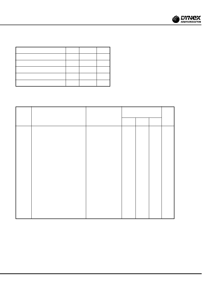
Figure 2: Electrical Characteristics
Figure 1: Absolute Maximum Ratings
DC CHARACTERISTICS AND RATINGS
Parameter
Min.
Max.
Units
Supply Voltage
-0.5
10
V
Input Voltage
-0.3
V
DD
+0.3
V
Current Through Any Pin
-25
+25
mA
Operating Temperature
-55
125
∞
C
Storage Temperature
-65
150
∞
C
Note: Stresses above those listed may cause permanent
damage to the device. This is a stress rating only and
functional operation of the device at these conditions, or at
any other condition above those indicated in the operations
section of this specification, is not implied. Exposure to
absolute maximum rating conditions for extended periods
may affect device reliability.
3/101
www.dynexsemi.com
54HSC/T Series
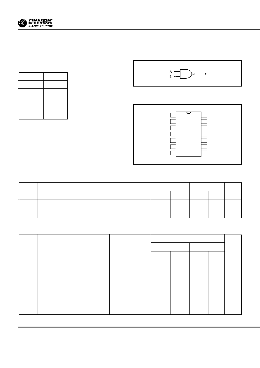
54HSC/T00 : Quadruple 2-Input Positive NAND Gates
Figure 2: Logic Diagram
Figure 3: Pin Out
14 VDD
13 4B
12 4A
11 4Y
10 3B
9 3A
8 3Y
1
1A
2
1B
3
1Y
4
2A
5
2B
6
2Y
7
VSS
Top
View
+25
∞
C
-55
∞
C / +125
∞
C
Symbol
Parameter
Typ.
Max.
Typ.
Max.
Units
t
PLH
Propagation delay time, low to high level output
11
20
17
22
ns
t
PHL
Propagation delay time, high to low level output
10
18
18
20
ns
The 54HSC/T00 is a Quadruple 2-Input Positive NAND gate.
Inputs
Outputs
A
B
Y
L
L
H
L
H
H
H
L
H
H
H
L
H = high level, L = low level
Figure 1: Function Table
Figure 4: Switching Characteristics
Figure 5: DC Characteristics
Limits
+25
∞
C
-55
∞
C / +125
∞
C
Symbol
Parameter
Test Conditions
Min.
Max.
Min.
Max.
Units
I
DD
Quiescent Current
V
IN
= 0V or V
DD
-
10
-
300
µ
A
V
OL
Output Voltage Low Level
I
OL
= 9mA
-
0.4
-
0.4
V
V
OH
Output Voltage High Level
I
OH
= -11mA
2.5
-
2.5
-
V
V
IL1
Voltage Input Low (CMOS)
-
-
1.5
-
1.5
V
V
IH1
Voltage Input High (CMOS)
-
3.5
-
3.5
-
V
V
IL2
Voltage Input Low (TTL)
-
-
0.8
-
0.8
V
V
IH2
Voltage Input High (TTL)
-
2.0
-
2.0
-
V
I
IN
Input Leakage Current
V
IN
= V
DD
or V
SS
-
±
0.5
-
±
5.0
µ
A

4/101
www.dynexsemi.com
54HSC/T Series
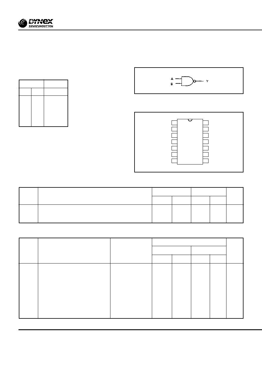
54HSC/T02 : Quadruple 2-Input Positive NOR Gates
Figure 2: Logic Diagram
Figure 3: Pin Out
The 54HSC/T02 is a Quadruple 2-Input Positive NOR gate.
Inputs
Outputs
A
B
Y
L
L
H
L
H
L
H
L
L
H
H
L
H = high level, L = low level
Figure 1: Function Table
14 VDD
13 4Y
12 4B
11 4A
10 3Y
9 3B
8 3A
1
1Y
2
1A
3
1B
4
2Y
5
2A
6
2B
7
VSS
Top
View
+25
∞
C
-55
∞
C / +125
∞
C
Symbol
Parameter
Typ.
Max.
Typ.
Max.
Units
t
PLH
Propagation delay time, low to high level output
11
20
17
22
ns
t
PHL
Propagation delay time, high to low level output
10
18
18
20
ns
Figure 4: Switching Characteristics
Figure 5: DC Characteristics
Limits
+25
∞
C
-55
∞
C / +125
∞
C
Symbol
Parameter
Test Conditions
Min.
Max.
Min.
Max.
Units
I
DD
Quiescent Current
V
IN
= 0V or V
DD
-
10
-
300
µ
A
V
OL
Output Voltage Low Level
I
OL
= 9mA
-
0.4
-
0.4
V
V
OH
Output Voltage High Level
I
OH
= -11mA
2.5
-
2.5
-
V
V
IL1
Voltage Input Low (CMOS)
-
-
1.5
-
1.5
V
V
IH1
Voltage Input High (CMOS)
-
3.5
-
3.5
-
V
V
IL2
Voltage Input Low (TTL)
-
-
0.8
-
0.8
V
V
IH2
Voltage Input High (TTL)
-
2.0
-
2.0
-
V
I
IN
Input Leakage Current
V
IN
= V
DD
or V
SS
-
±
0.5
-
±
5.0
µ
A
5/101
www.dynexsemi.com
54HSC/T Series
54HSC/T03 : Quadruple 2-Input Positive NAND Gates
With Open Collector Outputs
Figure 2: Logic Diagram
Figure 3: Pin Out
14 VDD
13 4B
12 4A
11 4Y
10 3B
9 3A
8 3Y
1
1A
2
1B
3
1Y
4
2A
5
2B
6
2Y
7
VSS
Top
View
+25
∞
C
-55
∞
C / +125
∞
C
Symbol
Parameter
Typ.
Max.
Typ.
Max.
Units
t
PLH
Propagation delay time, low to high level output
11
20
17
22
ns
t
PHL
Propagation delay time, high to low level output
10
18
18
20
ns
The 54HSC/T03 is a Quadruple 2-Input Positive NAND gate
with open collector output.
Inputs
Outputs
A
B
Y
L
L
H
L
H
H
H
L
H
H
H
L
H = high level, L = low level
Figure 1: Function Table
Figure 4: Switching Characteristics
Figure 5: DC Characteristics
Limits
+25
∞
C
-55
∞
C / +125
∞
C
Symbol
Parameter
Test Conditions
Min.
Max.
Min.
Max.
Units
I
DD
Quiescent Current
V
IN
= 0V or V
DD
-
10
-
300
µ
A
V
OL
Output Voltage Low Level
I
OL
= 9mA
-
0.4
-
0.4
V
V
OH
Output Voltage High Level
I
OH
= -11mA
2.5
-
2.5
-
V
V
IL1
Voltage Input Low (CMOS)
-
-
1.5
-
1.5
V
V
IH1
Voltage Input High (CMOS)
-
3.5
-
3.5
-
V
V
IL2
Voltage Input Low (TTL)
-
-
0.8
-
0.8
V
V
IH2
Voltage Input High (TTL)
-
2.0
-
2.0
-
V
I
IN
Input Leakage Current
V
IN
= V
DD
or V
SS
-
±
0.5
-
±
0.5
µ
A