
1/7
www.dynexsemi.com
DFM100PXM33-A000
FEATURES
s
Low Reverse Recovery Charge
s
High Switching Speed
s
Low Forward Voltage Drop
s
Isolated Base
s
MMC Baseplate With AlN Substrates
APPLICATIONS
s
Chopper Diodes
s
Boost and Buck Converters
s
Free-wheel Circuits
s
Snubber Circuits
s
Resonant Converters
s
Induction Heating
s
Multi-level Switch Inverters
The DFM100PXM33-A000 module houses a series
connected pair of 3300 volt, fast recovery diodes (FRDs).
Designed for low power loss, the module is suitable for a
variety of high voltage applications in motor drives and
power conversion. Configurations with common cathode
and common anode are available on request.
Fast switching times and low reverse recovery losses
allow high frequency operation making the device suitable
for the latest drive designs employing pwm and high
frequency switching.
These modules incorporate electrically isolated base
plates and low inductance construction enabling circuit
designers to optimise circuit layouts and utilise grounded
heat sinks for safety.
ORDERING INFORMATION
Order As:
DFM100PXM33-A000 - Series connection
DFM100PXM33-A005 - Common cathode
DFM100PXM33-A006 - Common anode
Note: When ordering, please use the complete part number.
DFM100PXM33-A000
Fast Recovery Diode Module
Preliminary Information
DS5564-1.1 October 2002
KEY PARAMETERS
V
RRM
3300V
V
F
(typ)
2.5V
I
F
(max)
100A
I
FM
(max)
200A
Fig. 1 Circuit diagrams
Fig. 2 Electrical connections - (not to scale)
Outline type code: P
(See package details for further information)
1(A2/K1)
2(K2)
3(A1)
Series connection, part number: DFM100PXM33-A000
1(K2/K1)
2(A2)
3(A1)
Common cathode, part number: DFM100PXM33-A005
1(A2/A1)
2(K2)
3(K1)
Common anode, part number: DFM100PXM33-A006

DFM100PXM33-A000
2/7
www.dynexsemi.com
Units
V
A
A
kA
2
s
W
kV
pC
ABSOLUTE MAXIMUM RATINGS
Stresses above those listed under 'Absolute Maximum Ratings' may cause permanent damage to the device. In extreme
conditions, as with all semiconductors, this may include potentially hazardous rupture of the package. Appropriate safety
precautions should always be followed. Exposure to Absolute Maximum Ratings may affect device reliability.
T
case
= 25∞C unless stated otherwise
Symbol
V
RRM
I
F
I
FM
I
2
t
Pmax
V
isol
Q
pd
Test Conditions
T
vj
= 125∞C
DC, T
case
= 70∞C
T
case
= 115∞C, t
p
= 1ms
V
R
= 0, t
p
= 10ms, T
vj
= 125∞C
T
case
= 25∞C, T
vj
= 125∞C
Commoned terminals to base plate. AC RMS, 1 min, 50Hz
IEC1287. V
1
= 2450V, V
2
= 1800V, 50Hz RMS
Max.
3300
100
200
10
463
6.0
10
Parameter
Repetitive peak reverse voltage
Forward current (per arm)
Max. forward current
I
2
t value fuse current rating
Maximum power dissipation
Isolation voltage
Partial discharge
Test Conditions
Continuous dissipation -
junction to case
Mounting torque 5Nm
(with mounting grease)
-
-
Mounting - M6
Electrical connections - M5
Parameter
Thermal resistance - diode (per arm)
Thermal resistance - case to heatsink
(per module)
Junction temperature
Storage temperature range
Screw torque
THERMAL AND MECHANICAL RATINGS
Symbol
R
th(j-c)
R
th(c-h)
T
j
T
stg
-
Units
∞C/kW
∞C/kW
∞C
∞C
Nm
Nm
Max.
216
16
125
125
5
4
Typ.
-
-
-
-
-
-
Min.
-
-
-
≠40
-
-
Internal insulation:
AlN
Baseplate material:
AlSiC
Creepage distance:
20mm
Clearance:
10mm
CTI (Critical Tracking Index): 175

3/7
www.dynexsemi.com
DFM100PXM33-A000
Test Conditions
V
R
= 3300V, T
vj
= 125∞C
I
F
= 100A
I
F
= 100A, T
vj
= 125∞C
-
Parameter
Peak reverse current
Forward voltage
Inductance
STATIC ELECTRICAL CHARACTERISTICS
T
vj
= 25∞C unless stated otherwise.
Symbol
I
RM
V
F
L
Units
mA
V
V
nH
Max.
10
-
-
-
Typ.
-
2.5
2.5
30
Min.
-
-
-
-
Test Conditions
I
F
= 100A,
dI
F
/dt = 600A/
µ
s,
V
R
= 1800V
Parameter
Reverse recovery current
Reverse recovery charge
Reverse recovery energy
Symbol
I
rr
Q
rr
E
rec
Units
A
µ
C
mJ
Max.
-
-
-
Typ.
85
60
65
Min.
-
-
-
DYNAMIC ELECTRICAL CHARACTERISTICS
T
vj
= 25∞C unless stated otherwise.
T
vj
= 125∞C unless stated otherwise.
Test Conditions
I
F
= 100A,
dI
F
/dt = 500A/
µ
s,
V
R
= 1800V
Parameter
Reverse recovery current
Reverse recovery charge
Reverse recovery energy
Symbol
I
rr
Q
rr
E
rec
Units
A
µ
C
mJ
Max.
-
-
-
Typ.
95
95
110
Min.
-
-
-

DFM100PXM33-A000
4/7
www.dynexsemi.com
TYPICAL CHARACTERISTICS
Fig. 2 Diode typical forward characteristics
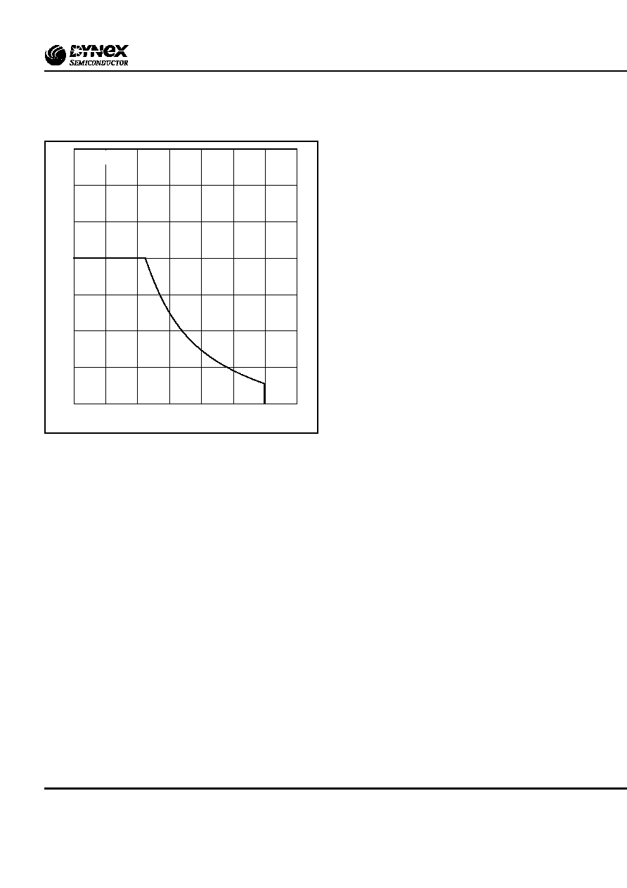
Fig. 4 Transient thermal impedance
Fig. 5 Power dissipation
Fig. 6DC current rating vs case temperature
0
50
100
150
200
250
300
350
400
450
500
0
25
50
75
100
125
150
Case temperature, T
case
- (∞C)
Power dissipation, P
tot
- (W)
0
25
50
75
100
125
150
175
0
25
50
75
100
125
150
Case temperature, T
case
- (∞C)
DC forward current, I
F
- (A)
1
10
100
1000
0.001
0.01
1
0.1
10
Pulse width, t
p
- (s)
Transient thermal impedance, Z
th (j-c)
- (
∞
C/kW )
R
i
(∞C/KW)
i
(ms)
1
5.909
0.0843
2
31.2918
3.7205
3
44.503
33.2138
4
134.6466
236.5275
0
25
50
75
100
125
150
175
200
0
0.5
1.0
1.5
2.0
2.5
3.0
3.5
4.0
Forward voltage, V
F
- (V)
Forward current, I
F
- (A)
T
j
= 25∞C
T
j
= 125∞C
V
F
is measured at power busbars
and not the auxiliary terminals
5/7
www.dynexsemi.com
DFM100PXM33-A000
Fig. 7 RBSOA
0
100
50
200
300
150
250
350
0
500
1000
1500
2000
2500
3000
3500
Reverse voltage, V
R
- (V)
Reverse recovery current, I
rr
- (A)
T
j
= 125∞C