 | –≠–ª–µ–∫—Ç—Ä–æ–Ω–Ω—ã–π –∫–æ–º–ø–æ–Ω–µ–Ω—Ç: DG858DW | –°–∫–∞—á–∞—Ç—å:  PDF PDF  ZIP ZIP |

DG858DW45
1/7
FEATURES
q
Double Side Cooling
q
High Reliability In Service
q
High Voltage Capability
q
Fault Protection Without Fuses
q
High Surge Current Capability
q
Turn-off Capability Allows Reduction In Equipment
Size And Weight. Low Noise Emission Reduces
Acoustic Cladding Necessary For Environmental
Requirements
APPLICATIONS
q
Variable speed A.C. motor drive inverters (VSD-AC).
q
Uninterruptable Power Supplies
q
High Voltage Converters.
q
Choppers.
q
Welding.
q
Induction Heating.
q
DC/DC Converters.
KEY PARAMETERS
I
TCM
3000A
V
DRM
4500V
I
T(AV)
1100A
dV
D
/dt
750V/
µ
s
dI
T
/dt
300A/
µ
s
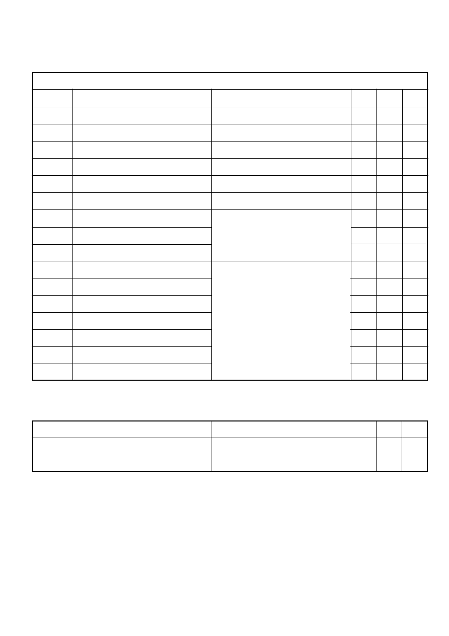
Fig.1 Package outline
Package outline type code : W
See Package Details for further information.
VOLTAGE RATINGS
4500
DG858DW45
Conditions
Type Number
T
vj
= 125
o
C, I
DRM
=100mA,
I
RRM
= 50mA
Repetitive Peak Off-state
Voltage
V
DRM
V
Repetitive Peak Reverse
Voltage
V
RRM
V
16
CURRENT RATINGS
Symbol
Parameter
Conditions
Max.
I
TCM
V
D
= V
DRM
, T
j
= 125
o
C, di
GQ
/dt = 40A/
µ
s,
Cs = 4.0
µ
F, L
S
200nH
A
3000
Units
Repetitive peak controllable on-state current
T
HS
= 80
o
C. Double side cooled, half sine 50Hz.
RMS on-state current
A
A
1100
1720
T
HS
= 80
o
C. Double side cooled, half sine 50Hz.
I
T(RMS)
I
T(AV)
Mean on-state current
DG858DW45
Gate Turn-Off Thyristor
Replaces July 1999 version, DS4334-4.0
DS4334-4.1 May 2000

DG858DW45
2/7
SURGE RATINGS
Conditions
20.0
2.0 x 10
6
kA
A
2
s
Surge (non-repetitive) on-state current
I
2
t for fusing
10ms half sine. T
j
= 125
o
C
10ms half sine. T
j
=125
o
C
di
T
/dt
Critical rate of rise of on-state current
300
20
V/
µ
s
Max.
Units
Rate of rise of off-state voltage
Peak stray inductance in snubber circuit
dV
D
/dt
200
nH
750
V/
µ
s
To 66% V
DRM
; V
RG
= -2V, T
j
= 125
o
C
I
TSM
Symbol
Parameter
I
2
t
V
D
= 3000V, I
T
= 3000A, T
j
=125
o
C
I
FG
> 40A, Rise time < 1.0
µ
s
A/
µ
s
To 66% V
DRM
; R
GK
22
, T
j
= 125
o
C
L
S
I
T
= 3000A, V
D
= V
DRM
, T
j
= 125∞C,
di
GQ
/dt = 40A/
µ
s, Cs = 4.0
µ
F
GATE RATINGS
Symbol
Parameter
Conditions
V
Units
Max.
16
20
Min.
-
20
-
Peak reverse gate voltage
Peak forward gate current
Average forward gate power
Peak reverse gate power
Rate of rise of reverse gate current
Minimum permissable on time
Minimum permissable off time
24
60
-
50
20
-
-
µ
s
100
100
V
RGM
This value maybe exceeded during turn-off
I
FGM
P
FG(AV)
P
RGM
di
GQ
/dt
t
ON(min)
t
OFF(min)
µ
s
A/
µ
s
kW
W
A
THERMAL AND MECHANICAL DATA
Symbol
Parameter
Conditions
Max.
Min.
R
th(c-hs)
Contact thermal resistance
R
th(j-hs)
-
-
0.03
-
0.0021
o
C/W
per contact
Cathode side cooled
Double side cooled
Units
-
0.011
o
C/W
Anode side cooled
o
C/W
0.017
Virtual junction temperature
T
OP
/T
stg
Operating junction/storage temperature range
-
Clamping force
-40
125
44.0
36.0
-40
kN
o
C/W
Clamping force 40kN
With mounting compound
DC thermal resistance - junction to
heatsink surface
T
vj
125
o
C
o
C
DG858DW45
3/7
CHARACTERISTICS
Conditions
Peak reverse current
On-state voltage
V
TM
Peak off-state current
Reverse gate cathode current
50
-
Turn-on energy
Gate trigger current
Delay time
Rise time
Fall time
Gate controlled turn-off time
Turn-off energy
Storage time
Turn-off gate charge
Total turn-off gate charge
Peak reverse gate current
-
12500
V
RGM
= 16V, No gate/cathode resistor
µ
C
I
T
= 3000A, V
DM
= 4200V
Snubber Cap Cs = 4.0
µ
F,
di
GQ
/dt = 40/
µ
s
T
j
= 125
o
C unless stated otherwise
Symbol
Parameter
I
DM
I
RRM
V
GT
Gate trigger voltage
I
GT
I
RGM
E
ON
t
d
t
r
E
OFF
t
gs
t
gf
t
gq
Q
GQ
Q
GQT
I
GQM
Min.
Max.
Units
At 3000A peak, I
G(ON)
= 10A d.c.
-
3.85
V
V
DRM
= 4500V, V
RG
= 2V
-
100
mA
At V
RRM
-
50
mA
V
D
= 24V, I
T
= 100A, T
j
= 25
o
C
-
1.2
V
V
D
= 24V, I
T
= 100A, T
j
= 25
o
C
-
4.0
A
mA
mJ
4400
-
V
D
= 2000V
I
T
= 3000A, dI
T
/dt = 300A/
µ
s
I
FG
= 40A, rise time < 1.0
µ
s
µ
s
2.0
-
-
6.0
µ
s
-
12500
mJ
-
26
µ
s
µ
s
2.5
-
µ
s
28.5
-
-
25000
µ
C
-
950
A
Conditions
Limit
V
dc
= 3500V, T
j
= -40 to + 125∞C,
ambient cosmic radiation at sea level, in
open air, 100% duty cycle.
Units
100
FIT
DC blocking reliability
RELIABILITY
DG858DW45
4/7
CURVES
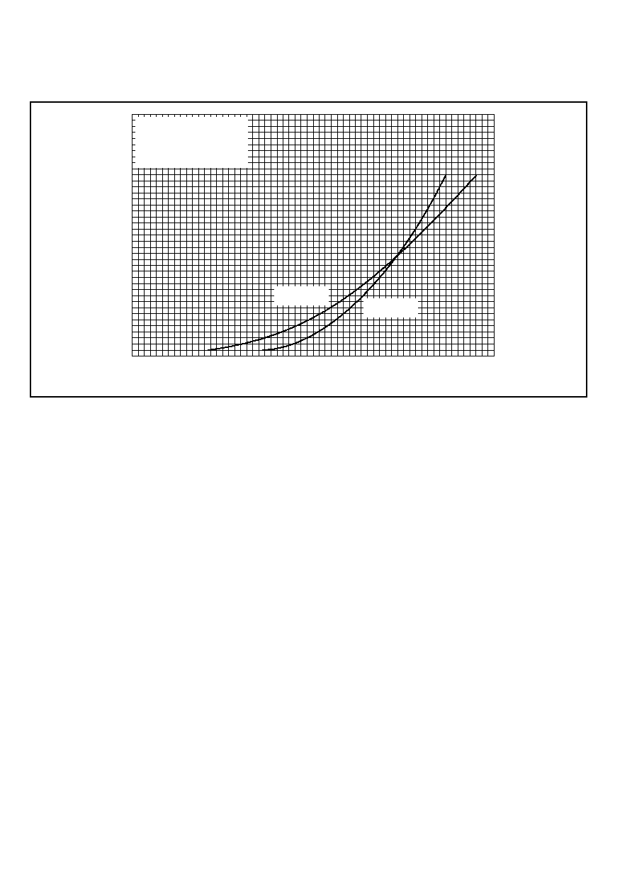
1.5
2.0
2.5
3.0
3.5
Instantaneous on-state voltage V
TM
- (V)
1000
2000
3000
4000
Instantaneous on-state current I
T
- (A)
Measured under pulse
conditions.
I
G(ON)
= 10A
Half sine wave 10ms
0
4.0
1.0
T
j
= 125∞C
T
j
= 25∞C
Figure 2. On-state characteristics

DG858DW45
5/7
Recommended gate conditions:
I
TCM
= 3000A
I
FG
= 40A
I
G(ON)
= 10A d.c.
t
w1(min)
= 20
µ
s
I
GQM
= 1200A
di
GQ
/dt = 40A/
µ
s
Q
GQ
= 12500
µ
C
V
RG(min)
= 2V
V
RG(max)
= 18V
Anode voltage and current
VD
0.9VD
0.1VD
td
tr
tgt
IT
VDP
0.9IT
ITAIL
dVD/dt
VD VDM
Gate voltage and current
tgs
tgf
tw1
VFG
IFG
0.1IFG
dIFG/dt
0.1IGQ
QGQ
0.5IGQM
IGQM
VRG
V(RG)BR
IG(ON)
tgq
These are recommended Dynex Semiconductor conditions. Other conditions are permitted
according to users gate drive specifications.
Figure 3. General switching waveforms