
DIM2400NSM12-E000
Caution: This device is sensitive to electrostatic discharge. Users should follow ESD handling procedures.
1/9
www.dynexsemi.com
Replaces April 2004 version, issue PDS5758-1.0
PDS5758-2.0 April 2004
FEATURES
I
Trench Gate Field Stop Technology
I
Low Conduction Losses
I
Low Switching Losses
I
10
µ
s Short Circuit Withstand
I
Isolated MMC Base with AlN Substrates
I
High Thermal Cycling Capability
APPLICATIONS
I
High Reliability Inverters
G
Wind Turbines
G
Motor Controllers
G
UPS Systems
I
Traction
G
Propulsion Drives
G
Auxiliaries
The Powerline range of high power modules includes half
bridge, chopper, dual, single and bi-directional switch
configurations covering voltages from 600V to 3300V and
currents up to 3600A.
The DIM2400NSM12-E000 is a single switch 1200V, n
channel enhancement mode, insulated gate bipolar transistor
(IGBT) module. The IGBT has a wide reverse bias safe
operating area (RBSOA) plus full 10
µ
s short circuit withstand.
This module is optimised for applications requiring high thermal
cycling capability.
The module incorporates an electrically isolated base plate
and low inductance construction enabling circuit designers to
optimise circuit layouts and utilise grounded heat sinks for safety.
ORDERING INFORMATION
Order As:
DIM2400NSM12-E000
Note: When ordering, please use the complete part number.
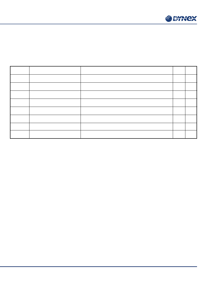
KEY PARAMETERS
V
CES
1200V
V
CE(sat)
*
(typ)
1.7V
I
C
(max)
2400A
I
C(PK)
(max)
4800A
*
Measured at auxiliary terminals.
DIM2400NSM12-E000
Single Switch IGBT Module
Fig. 1 Single switch circuit diagram
Fig. 2 Module Outline
Outline type code: N
(See package details for further information)
C2
C1
Aux C
G
Aux E
E1
E2
External connection
External connection
C1
E1
C2
E2
G
E
2
C
1
E
2
- Aux Emitter
C
1
- Aux Collector
DIM2400NSM12-E000
2/9
Caution: This device is sensitive to electrostatic discharge. Users should follow ESD handling procedures.
www.dynexsemi.com
Test Conditions
V
GE
= 0V
-
T
case
= 70∞C
1ms, T
case
= 110∞C
T
case
= 25∞C, T
j
= 150∞C
V
R
= 0, t
p
= 10ms, T
vj
= 125∞C
Commoned terminals to base plate. AC RMS, 1 min, 50Hz
IEC1287. V
1
= 1300V, V
2
= 1000V, 50Hz RMS
Symbol
V
CES
V
GES
I
C
I
C(PK)
P
max
I
2
t
V
isol
Q
PD
ABSOLUTE MAXIMUM RATINGS
Stresses above those listed under 'Absolute Maximum Ratings' may cause permanent damage to the device. In extreme
conditions, as with all semiconductors, this may include potentially hazardous rupture of the package. Appropriate safety precautions
should always be followed. Exposure to Absolute Maximum Ratings may affect device reliability.
T
case
= 25∞C unless stated otherwise
Units
V
V
A
A
kW
kA
2
s
V
PC
Max.
1200
±
20
2400
4800
10.4
400
2500
10
Parameter
Collector-emitter voltage
Gate-emitter voltage
Continuous collector current
Peak collector current
Max. transistor power dissipation
Diode I
2
t value
Isolation voltage - per module
Partial discharge - per module
DIM2400NSM12-E000
Caution: This device is sensitive to electrostatic discharge. Users should follow ESD handling procedures.
3/9
www.dynexsemi.com
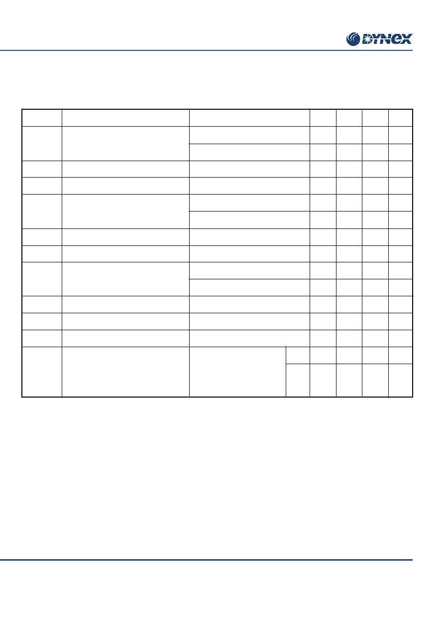
Test Conditions
Continuous dissipation -
junction to case
Continuous dissipation -
junction to case
Mounting torque 5Nm
(with mounting grease)
Transistor
Diode
-
Mounting - M6
Electrical connections - M4
Electrical connections - M8
Parameter
Thermal resistance - transistor
Thermal resistance - diode
Thermal resistance - case to heatsink
(per module)
Junction temperature
Storage temperature range
Screw torque
THERMAL AND MECHANICAL RATINGS
Internal insulation material:
AlN
Baseplate material:
AlSiC
Creepage distance:
33mm
Clearance:
20mm
CTI (Critical Tracking Index): 175
Symbol
R
th(j-c)
R
th(j-c)
R
th(c-h)
T
j
T
stg
-
Units
∞C/kW
∞C/kW
∞C/kW
∞C
∞C
∞C
Nm
Nm
Nm
Max.
12
20
8
150
125
125
5
2
10
Typ.
-
-
-
-
-
-
-
-
-
Min.
-
-
-
-
-
≠40
-
-
-
DIM2400NSM12-E000
4/9
Caution: This device is sensitive to electrostatic discharge. Users should follow ESD handling procedures.
www.dynexsemi.com
Test Conditions
V
GE
= 0V, V
CE
= V
CES
V
GE
= 0V, V
CE
= V
CES
, T
case
= 125∞C
V
GE
=
±
20V, V
CE
= 0V
I
C
= 96mA, V
GE
= V
CE
V
GE
= 15V, I
C
= 2400A
V
GE
= 15V, I
C
= 2400A, , T
case
= 125∞C
DC
t
p
= 1ms
I
F
= 2400A
I
F
= 2400A, T
case
= 125∞C
V
CE
= 25V, V
GE
= 0V, f = 1MHz
-
-
T
j
= 125∞C, V
CC
= 1000V,
I
1
t
p
10
µ
s, V
CE(max)
= V
CES
≠ L*. di/dt
I
2
IEC 60747-9
Parameter
Collector cut-off current
Gate leakage current
Gate threshold voltage
Collector-emitter saturation voltage
Diode forward current
Diode maximum forward current
Diode forward voltage
Input capacitance
Module inductance
Internal transistor resistance
Short circuit. I
SC
ELECTRICAL CHARACTERISTICS
T
case
= 25∞C unless stated otherwise.
Symbol
I
CES
I
GES
V
GE(TH)
V
CE(sat)
I
F
I
FM
V
F
C
ies
L
M
R
INT
SC
Data
Units
mA
mA
µ
A
V
V
V
A
A
V
V
nF
nH
m
A
A
Max.
5
25
4
6.5
2.15
2.5
2400
4800
2.5
3.0
-
-
-
-
-
Typ.
-
-
-
5.8
1.7
2.0
-
-
2.1
2.4
172
16
0.15
9600
8250
Min.
-
-
-
5.0
-
-
-
-
-
-
-
-
-
-
-
Note:
Measured at auxiliary terminals.
* L is the circuit inductance + L
M

DIM2400NSM12-E000
Caution: This device is sensitive to electrostatic discharge. Users should follow ESD handling procedures.
5/9
www.dynexsemi.com
Units
ns
ns
mJ
ns
ns
mJ
µ
C
µ
C
A
mJ
Max.
-
-
-
-
-
-
-
-
-
-
Typ.
700
200
300
600
300
280
24
240
800
84
Min.
-
-
-
-
-
-
-
-
-
-
Test Conditions
I
C
= 2400A
V
GE
=
±
15V
V
CE
= 600V
R
G(ON)
= 1.2
R
G(OFF)
= 0.3
L ~ 30nH
I
F
= 2400A, V
R
= 600V,
dI
F
/dt = 4250A/
µ
s
Parameter
Turn-off delay time
Fall time
Turn-off energy loss
Turn-on delay time
Rise time
Turn-on energy loss
Gate charge
Diode reverse recovery charge
Diode reverse current
Diode reverse recovery energy
ELECTRICAL CHARACTERISTICS
T
case
= 25∞C unless stated otherwise
Symbol
t
d(off)
t
f
E
OFF
t
d(on)
t
r
E
ON
Q
g
Q
rr
I
rr
E
REC
T
case
= 125∞C unless stated otherwise
Units
ns
ns
mJ
ns
ns
mJ
µ
C
A
mJ
Max.
-
-
-
-
-
-
-
-
-
Typ.
820
250
400
600
300
480
500
1000
200
Min.
-
-
-
-
-
-
-
-
-
Test Conditions
I
C
= 2400A
V
GE
=
±
15V
V
CE
= 600V
R
G(ON)
= 1.2
R
G(OFF)
= 0.3
L ~ 30nH
I
F
= 2400A, V
R
= 600V,
dI
F
/dt = 4250A/
µ
s
Parameter
Turn-off delay time
Fall time
Turn-off energy loss
Turn-on delay time
Rise time
Turn-on energy loss
Diode reverse recovery charge
Diode reverse current
Diode reverse recovery energy
Symbol
t
d(off)
t
f
E
OFF
t
d(on)
t
r
E
ON
Q
rr
I
rr
E
REC
Note:
Switching Characteristic measurements taken using standard driver circuit conditions.