
DIM500BSS06-S000
Caution: This device is sensitive to electrostatic discharge. Users should follow ESD handling procedures.
1/9
www.dynexsemi.com
DS5677-1.3 February 2004
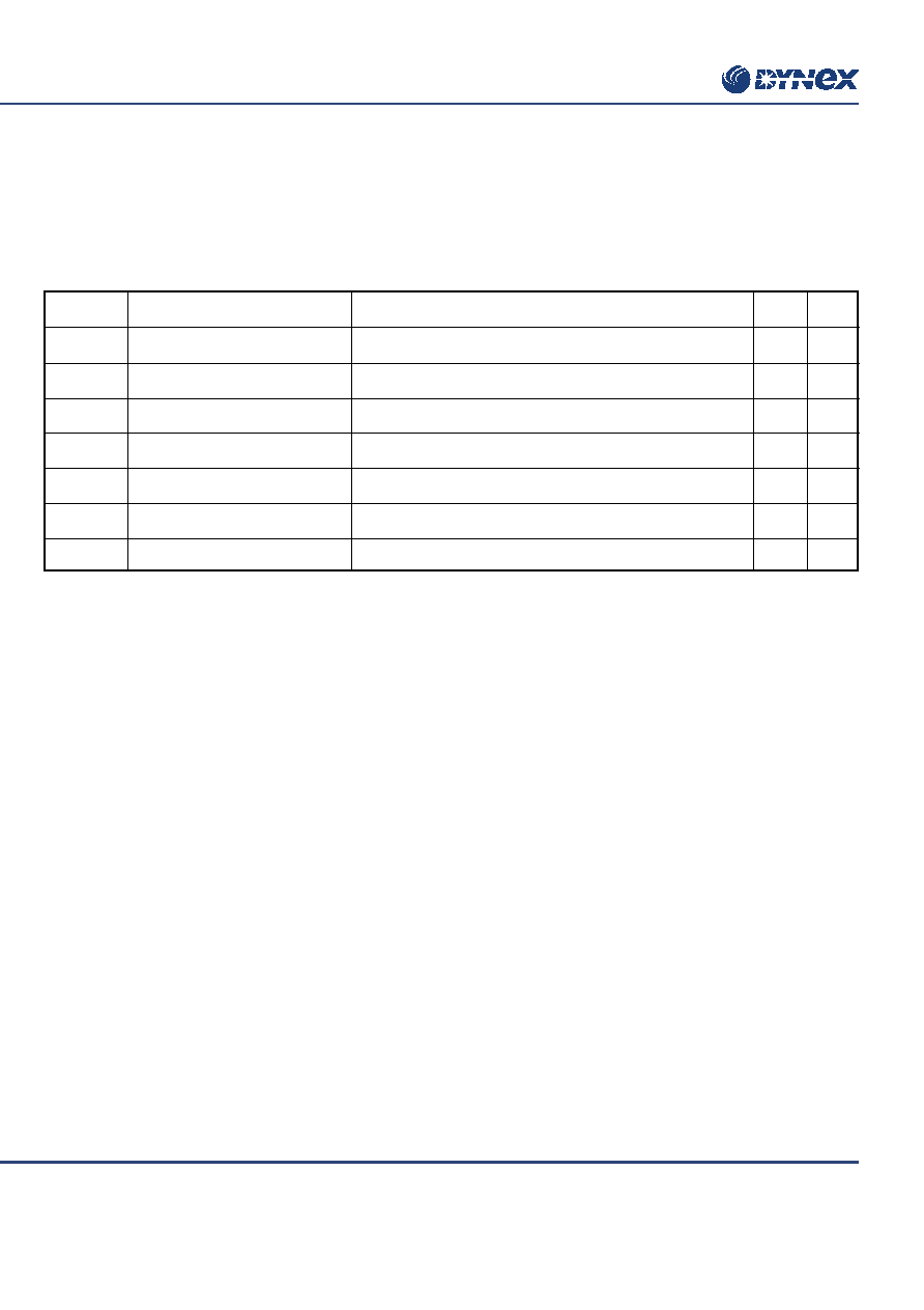
KEY PARAMETERS
V
CES
600V
V
CE(sat)
*
(typ)
2.1V
I
C
(max) 500A
I
C(PK)
(max) 1000A
*(measured at the power busbars and not the auxiliary terminals)
FEATURES
I
n - Channel
I
High Switching Speed
I
Low Forward Voltage Drop
I
Isolated Base
APPLICATIONS
I
PWM Motor Contro
l
I
UPS
The Powerline range of modules includes half bridge,
chopper, bi-directional, dual and single switch configurations
covering voltages from 600V to 3300V and currents up to 3600A.
The DIM500BSS06-S000 is a single switch 600V n channel
enhancement mode insulated gate bipolar transistor (IGBT)
module. The module is suitable for a variety of medium voltage
applications in motor drives and power conversion.
The IGBT has a wide reverse bias safe operating area
(RBSOA) for ultimate reliability in demanding applications.
These modules incorporate electrically isolated base plates
and low inductance construction enabling circuit designers to
optimise circuit layouts and utilise earthed heat sinks for safety.
Typical applications include dc motor drives, ac pwm
drivesand ups systems.
ORDERING INFORMATION
Order as:
DIM500BSS06-S000
Note: When ordering, use complete part number.
DIM500BSS06-S000
Single Switch IGBT Module
Fig. 1 Single switch circuit diagram
Fig. 2 Module outline
Outline type code: B
(See package details for further information)
2(E)
3(G
1
)
1(C)
5(E
1
)
4(C
1
)
DIM500BSS06-S000
2/9
Caution: This device is sensitive to electrostatic discharge. Users should follow ESD handling procedures.
www.dynexsemi.com
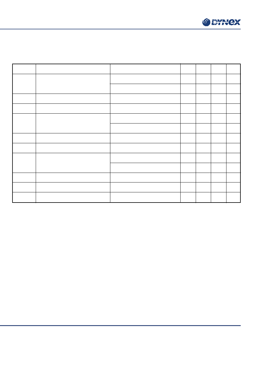
Test Conditions
V
GE
= 0V
-
T
case
= 65∞C
1ms, T
case
= 95∞C
T
case
= 25∞C, T
j
= 150∞C
V
R
= 0, t
p
= 10ms, T
vj
= 125∞C
Commoned terminals to base plate. AC RMS, 1 min, 50Hz
Symbol
V
CES
V
GES
I
C
I
C(PK)
P
max
I
2
t
V
isol
ABSOLUTE MAXIMUM RATINGS - PER ARM
Stresses above those listed under 'Absolute Maximum Ratings' may cause permanent damage to the device. In extreme
conditions, as with all semiconductors, this may include potentially hazardous rupture of the package. Appropriate safety precautions
should always be followed. Exposure to Absolute Maximum Ratings may affect device reliability.
T
case
= 25∞C unless stated otherwise
Units
V
V
A
A
W
kA
2
s
kV
Max.
600
±
20
500
1000
2907
TBD
2.5
Parameter
Collector-emitter voltage
Gate-emitter voltage
Continuous collector current
Peak collector current
Max. transistor power dissipation
Diode I
2
t value
Isolation voltage - per module

DIM500BSS06-S000
Caution: This device is sensitive to electrostatic discharge. Users should follow ESD handling procedures.
3/9
www.dynexsemi.com
Test Conditions
Continuous dissipation -
junction to case
Continuous dissipation -
junction to case
Mounting torque 5Nm
(with mounting grease)
Transistor
Diode
-
Mounting - M6
Electrical connections - M3
Electrical connections - M4
Parameter
Thermal resistance - transistor
Thermal resistance - diode
Thermal resistance - case to heatsink
(per module)
Junction temperature
Storage temperature range
Screw torque
THERMAL AND MECHANICAL RATINGS
Internal insulation:
Al
2
O
3
Clearance:
11mm
Baseplate material:
Cu
CTI (Critical Tracking Index):
425
Creepage distance:
20mm
Symbol
R
th(j-c)
R
th(j-c)
R
th(c-h)
T
j
T
stg
-
Units
∞C/kW
∞C/kW
∞C/kW
∞C
∞C
∞C
Nm
Nm
Nm
Max.
43
81
15
150
125
125
5
5
2
Typ.
-
-
-
-
-
-
-
-
Min.
-
-
-
-
-
≠40
3
2.5
1.1
DIM500BSS06-S000
4/9
Caution: This device is sensitive to electrostatic discharge. Users should follow ESD handling procedures.
www.dynexsemi.com
Note:
Measured at the power busbars and not the auxiliary terminals.
L* is the circuit inductance + L
M
Test Conditions
V
GE
= 0V, V
CE
= V
CES
V
GE
= 0V, V
CE
= V
CES
, T
case
= 125∞C
V
GE
=
±
20V, V
CE
= 0V
I
C
= 20mA, V
GE
= V
CE
V
GE
= 15V, I
C
= 375A
V
GE
= 15V, I
C
= 375A, , T
case
= 125∞C
DC
t
p
= 1ms
I
F
= 50A
I
F
= 500A, T
case
= 125∞C
V
CE
= 25V, V
GE
= 0V, f = 1MHz
-
-
Parameter
Collector cut-off current
Gate leakage current
Gate threshold voltage
Collector-emitter saturation voltage
Diode forward current
Diode maximum forward current
Diode forward voltage
Input capacitance
Module inductance
Internal transistor resistance - per arm
ELECTRICAL CHARACTERISTICS
T
case
= 25∞C unless stated otherwise.
Symbol
I
CES
I
GES
V
GE(TH)
V
CE(sat)
I
F
I
FM
V
F
C
ies
L
M
R
INT
Units
mA
mA
µ
A
V
V
V
A
A
V
V
nF
nH
m
Max.
3
15
3
7.5
2.6
2.8
500
1000
1.8
1.8
-
-
Typ.
-
-
-
5.5
2.1
2.3
-
-
1.5
1.5
54
20
0.23
Min.
-
-
-
4.5
-
-
-
-
-
-
-
-
-
DIM500BSS06-S000
Caution: This device is sensitive to electrostatic discharge. Users should follow ESD handling procedures.
5/9
www.dynexsemi.com
Units
ns
ns
mJ
ns
ns
mJ
µ
C
µ
C
A
mJ
Max.
-
-
-
-
-
-
-
-
-
-
Typ.
600
250
45
490
150
30
4
30
240
9
Min.
-
-
-
-
-
-
-
-
-
-
Test Conditions
I
C
= 500A
V
GE
=
±
15V
V
CE
= 300V
R
G(ON)
= R
G(OFF)
= 4.7
L ~ 100nH
I
F
= 500A, V
R
= 300V,
dI
F
/dt = 2800A/
µ
s
Parameter
Turn-off delay time
Fall time
Turn-off energy loss
Turn-on delay time
Rise time
Turn-on energy loss
Gate charge
Diode reverse recovery charge
Diode reverse current
Diode reverse recovery energy
ELECTRICAL CHARACTERISTICS
T
case
= 25∞C unless stated otherwise
Symbol
t
d(off)
t
f
E
OFF
t
d(on)
t
r
E
ON
Q
g
Q
rr
I
rr
E
REC
T
case
= 125∞C unless stated otherwise
Units
ns
ns
mJ
ns
ns
mJ
µ
C
A
mJ
Max.
-
-
-
-
-
-
-
-
-
Typ.
650
500
65
550
150
50
40
265
10
Min.
-
-
-
-
-
-
-
-
-
Test Conditions
I
C
= 500A
V
GE
=
±
15V
V
CE
= 300V
R
G(ON)
= R
G(OFF)
= 4.7
L ~ 100nH
I
F
= 500A, V
R
= 300V,
dI
F
/dt = 2800A/
µ
s
Parameter
Turn-off delay time
Fall time
Turn-off energy loss
Turn-on delay time
Rise time
Turn-on energy loss
Diode reverse recovery charge
Diode reverse current
Diode reverse recovery energy
Symbol
t
d(off)
t
f
E
OFF
t
d(on)
t
r
E
ON
Q
rr
I
rr
E
REC