Linear Integrated Systems
Linear Integrated Systems
4042 Clipper Ct., Fremont, CA 94538 TEL: (510) 490-9160 ∑ FAX: (510) 353-0261
ULTRA-HIGH INPUT IMPEDANCE
N-CHANNEL JFET
LS4117, 4118, 4119
FEATURES
LOW POWER
I
DSS
<90
µ
A (2N4117)
MINIMUM CIRCUIT LOADING
I
GSS
<1 pA (2N4117A Series)
ABSOLUTE MAXIMUM RATINGS (NOTE 1)
@ 25
∞
C (unless otherwise noted)
Gate-Source or Gate-Drain Voltage (NOTE 1)
-40V
Gate-Current
50mA
Total Device Dissipation
(Derate 2mW/
∞
C to 175
∞
C)
300mW
Storage Temperature Range
-65
∞
C to +175
∞
C
Lead Temperature
(1/16" from case for 10 seconds)
255
∞
C
ELECTRICAL CHARACTERISTICS @ 25
∞
C (unless otherwise noted)
2N4117/A
2N4118
2N4119
FN4117/A
2N4118A
2N4119A
SYMBOL CHARACTERISTICS MIN MAX MIN MAX MIN MAX UNITS CONDITIONS
I
GSS
Gate Reverse Current
--
-10
--
-10
--
-10
pA
V
GS
= -20V V
DS
= 0
Standard only
--
-25
--
-25
--
-25
nA
I
GSS
Gate Reverse Current
--
-1
--
-1
--
-1
pA
V
GS
=-20V V
DS
= 0
"A" Series only
--
-2.5
--
-2.5
--
-2.5
nA
BV
GSS
Gate-Source Breakdown Voltage
-40
--
-40
--
-40
--
I
G
=-1
µ
A
V
DS
= 0
V
GS(off)
Gate-Source Cutoff Voltage
-0.6
-1.8
-1
-3
-2
-6
V
DS
=10V
I
D
= 1nA
I
DSS
Saturation Drain Current
0.03
0.09
0.08
0.24
0.20
0.60
mA
V
DS
=10V
V
GS
= 0
(NOTE 2) FN4117/A 0.015
g
fs
Common-Source Forward
70
210
80
250
100
330
Transconductance (NOTE 2)
g
os
Common-Source Output
--
3
--
5
--
10
Conductance
C
iss
Common-Source Input
--
3
--
3
--
3
V
DS
= 10V V
GS
= 0
Capacitance
C
rss
Common-Source Reverse
--
1.5
--
1.5
--
1.5
Transfer Capacitance
150
∞
C
150
∞
C
V
µ
mho
pF
f=1MHz
f=1kHz
NOTES:
1. Due to symmetrical geometry, these units may be operated with source and drain leads interchanged.
2. This parameter is measured during a 2 ms interval 100 ms after power is applied. (Not a JEDEC condition.)
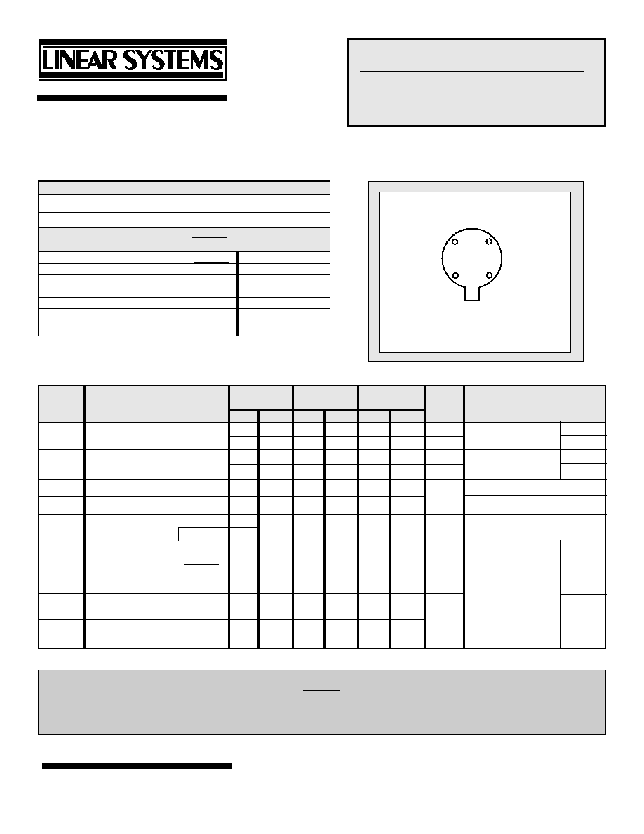
1
2
3
4
Case
G
D
S
TO-72
Bottom View
D
S
G
C