FEATURES
HIGH INPUT IMPEDANCE
r
Gs
= 100G
HIGH TRANSCONDUCTANCE
Y
FS
= 30,000µS
ABSOLUTE MAXIMUM RATINGS
1
@ 25 ∞C (unless otherwise stated)
Maximum Temperatures
Storage Temperature
-65 to +150 ∞C
Operating Junction Temperature
-55 to +125 ∞C
Maximum Power Dissipation
Continuous Power Dissipation @ +125 ∞C
200mW
Maximum Currents
Drain Current
I
D
= 25mA
Maximum Voltages
Drain to Source
1
V
DSO
= 20V
Gate to Source
V
GSS
= 20V
ELECTRICAL CHARACTERISTICS @ 25 ∞C (unless otherwise stated)
SYMBOL CHARACTERISTIC
MIN
TYP MAX UNITS
CONDITIONS
V
DS
Drain to Source Voltage
-20
V
I
DS
= 100µA, V
GS
= 0V
V
GS
Gate to Source Voltage
-12
-10
-7
V
I
DS
= 10mA, V
gs
= -10V
2,3
g
fs
Common Source Forward Transconductance 30,000
µS
I
DS
= 10mA, V
DS
= -10V, f = 1kHz
g
oss
Common Source Output Conductance
300
µS
I
DS
= 10mA, V
DS
= -10V, f = 1kHz
r
Gs
Gate to Source Input Resistance
100
G
V
GS
= 0 to 20V, T
J
to 125 ∞C
C
ISS
Input
Capacitance
8 pF I
DS
= 10mA, V
DS
= -10V
C
RSS
Reverse Transfer Capacitance
1.5
pF
I
DS
= 10mA, V
DS
= -10V
e
n
Noise
Voltage
25 µV
I
DS
= 10mA, V
DS
= 10V
BW = 50 to 15kHz
LS320
HIGH INPUT IMPEDANCE
BiFET AMPLIFIER
Linear Integrated Systems
PACKAGE OPTIONS
G
S
D
TO-92
BOTTOM VIEW
1
2
3
D S G
1
2
3
SOT-23
TOP VIEW
D
S
G
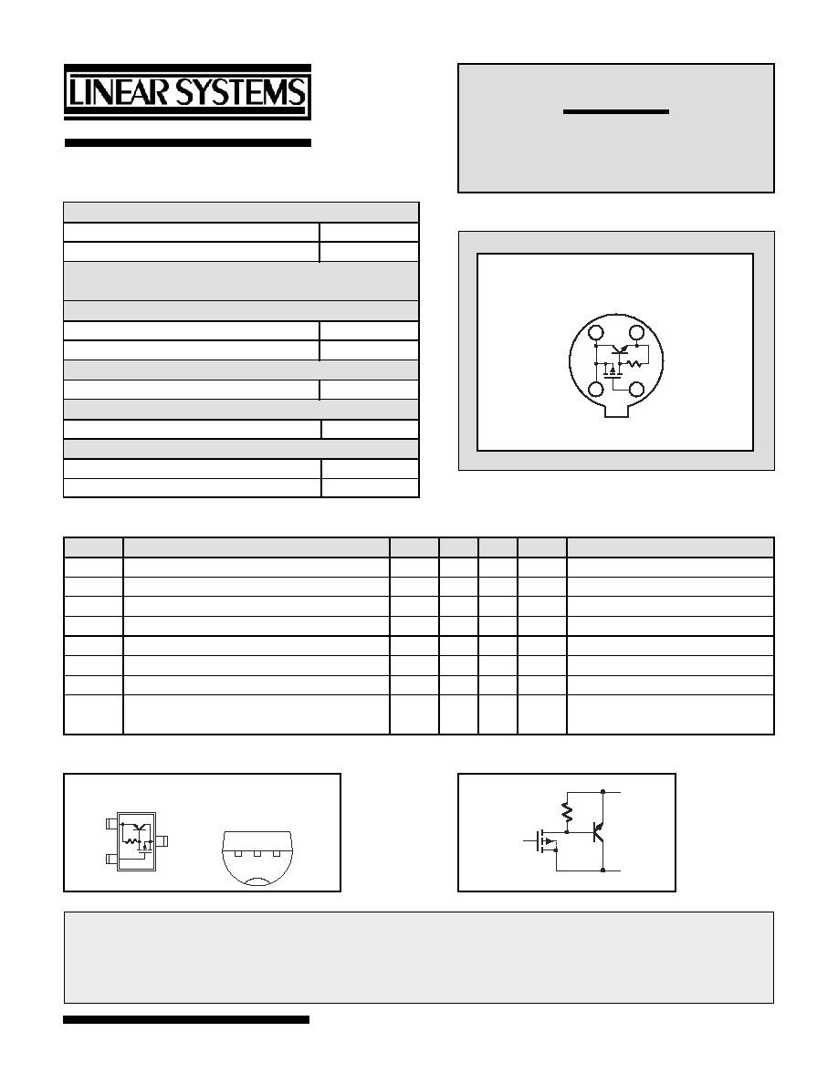
FUNCTIONAL SCHEMATIC
S
S
D
2
1
3
BOTTOM VIEW
TO-72
4
G
1.
Absolute maximum ratings are limiting values above which serviceability may be impaired.
2.
The gate to source voltage must never exceed 100V, t < 10ms.
3.
Additional screening available
Information furnished by Linear Integrated Systems is believed to be accurate and reliable. However, no responsibility is assumed for its
use; nor for any infringement of patents or other rights of third parties which may result from its use. No license is granted by implicatio
otherwise under any patent or patent rights of Linear Integrated Systems.
n or
Linear Integrated Systems
∑ 4042 Clipper Court ∑ Fremont, CA 94538 ∑ Tel: 510 490-9160 ∑ Fax: 510 353-0261