FEATURES
DIRECT REPLACEMENT FOR CRYSTALONICS FF627
FLAT GLASS TOP FOR EXTERNAL OPTICS
ULTRA HIGH SENSITIVITY
ABSOLUTE MAXIMUM RATINGS
1
@ 25 ∞C (unless otherwise stated)
Maximum Temperatures
Storage Temperature
-65 to +200 ∞C
Operating Junction Temperature
-55 to +165 ∞C
Maximum Power Dissipation
Continuous Power Dissipation
400mW
Maximum Currents
Gate Current
50mA
Maximum Voltages
Drain to Source
15V
Drain to Gate
15V
Gate to Source
-10V
ELECTRICAL CHARACTERISTICS @ 25 ∞C (unless otherwise stated)
SYMBOL
CHARACTERISTIC
MIN TYP MAX
UNITS
CONDITIONS
V
GS(off)
Gate to Source Cutoff Voltage (V
PO
)
1.0 5.0
V
V
DS
= 10V, I
D
= 0.1µA
S
G
Gate
Sensitivity
2
6.4
24
µA/mW/cm
2
V
DS
= 10V, V
GS
= 0V,
= 0.9µm
S
D
Drain
Sensitivity
3
500
mA/mW/cm
2
V
DS
= 10V, V
GS
= 0V, R
G
= 1M
Ig
Gate Current (Light)
4
10
37.5
nA/FC
V
DS
= 10V, V
GS
= 0V
Id
Drain Current (Light)
4
800
µA/FC
V
DS
= 10V, V
GS
= 0V, R
G
= 1M
I
DSS
Drain Saturation Current
8.0
mA
V
DS
= 10V, V
GS
= 0V
I
GSS
Gate Leakage Current (Dark)
30
pA
V
GS
= -10V, V
DS
= 0V
g
fs
Forward Transconductance (g
m
) 8000
µS V
DS
= 10V, V
GS
= 0V, f = 1kHz
R
DS(on)
Drain to Source On Resistance
100
V
DS
= 0.1V, V
GS
= 0V
C
GS
Gate to Source Capacitance
35
V
GS
= -10V, f = 140kHz
C
GD
Gate to Drain Capacitance
20
pF
V
GD
= -10V,
f
= 140kHz
t
r
Rise
Time
5
30
t
f
Fall
Time
6
50
ns V
DS
= 10V, R
L
= R
G
= 100
D
S
G
2
1
3
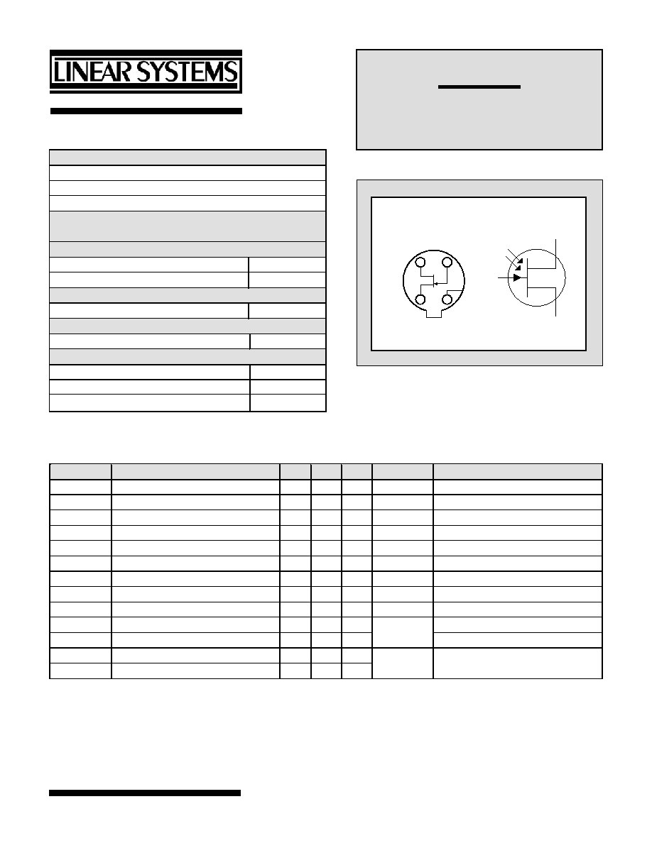
BOTTOM VIEW
TO-72
4
C
Linear Integrated Systems
LS627
PHOTO FET
LIGHT SENSITIVE JFET
Linear Integrated Systems
∑ 4042 Clipper Court ∑ Fremont, CA 94538 ∑ Tel: 510 490-9160 ∑ Fax: 510 353-0261
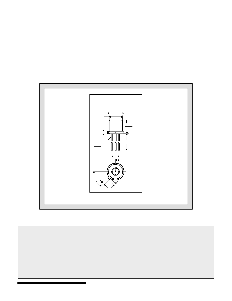
TO-72
Four Lead
0.230
0.209
DIA.
DIA.
0.195
0.175
0.030
MAX.
0.500 MIN.
0.150
0.115
0.019
0.016
DIA.
4 LEADS
2
1
3
0.046
0.036
45∞
0.048
0.028
0.100
0.050
4
Linear Integrated Systems
∑ 4042 Clipper Court ∑ Fremont, CA 94538 ∑ Tel: 510 490-9160 ∑ Fax: 510 353-0261
NOTES
1.
Absolute maximum ratings are limiting values above which serviceability may be impaired.
2.
Gate Current per unit Radient Power Density at Lens Surface
3.
Drain Current per unit Radient Power Density (
= 0.9µm).
4.
Tungsten Lamp 2800∞K Color Temperature.
5.
GaAs Diode Source.
6.
Directly Proportional to R
G
.
7.
Not production tested. Guaranteed by design.
Information furnished by Linear Integrated Systems is believed to be accurate and reliable. However, no responsibility is assumed for its
use; nor for any infringement of patents or other rights of third parties which may result from its use. No license is granted by implicatio
otherwise under any patent or patent rights of Linear Integrated Systems.
n or