 | –≠–ª–µ–∫—Ç—Ä–æ–Ω–Ω—ã–π –∫–æ–º–ø–æ–Ω–µ–Ω—Ç: LTBDM | –°–∫–∞—á–∞—Ç—å:  PDF PDF  ZIP ZIP |
1
LT3470
3470f
Automotive Battery Regulation
Power for Portable Products
Distributed Supply Regulation
Industrial Supplies
Wall Transformer Regulation
Micropower Buck Regulator
with Integrated Boost and
Catch Diodes
Low Quiescent Current: 26
µ
A at 12V
IN
to 3.3V
OUT
Integrated Boost and Catch Diodes
Input Range: 4V to 40V
Low Output Ripple: <10mV
< 1µA in Shutdown Mode
Output Voltage: 1.25V to 16V
200mA Output Current
Hysteretic Mode Control
≠ Low Ripple Burst Mode
Æ
Operation at Light Loads
≠ Continuous Operation at Higher Loads
Solution Size as Small as 50mm
2
Low Profile (1mm) ThinSOT Package
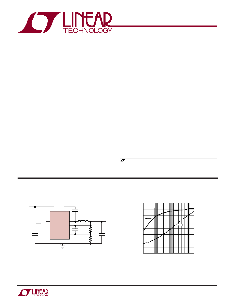
Efficiency and Power Loss vs Load Current
Burst Mode is a registered trademark of Linear Technology Corporation.
ThinSOT is a trademark of Linear Technology Corporation.
FEATURES
DESCRIPTIO
U
APPLICATIO S
U
TYPICAL APPLICATIO
U
The LT
Æ
3470 is a micropower step-down DC/DC converter
that integrates a 300mA power switch, catch diode and
boost diode into a low profile (1mm) ThinSOT
TM
package.
The LT3470 combines Burst Mode and continuous opera-
tion to allow the use of tiny inductor and capacitors while
providing a low ripple output to loads of up to 200mA.
With its wide input range of 4V to 40V, the LT3470 can
regulate a wide variety of power sources, from 2-cell
Li-Ion batteries to unregulated wall transformers and lead-
acid batteries. Quiescent current in regulation is just 26µA
in a typical application while a zero current shutdown
mode disconnects the load from the input source, simpli-
fying power management in battery-powered systems.
Fast current limiting and hysteretic control protects the
LT3470 and external components against shorted out-
puts, even at 40V input.
LOAD CURRENT (mA)
30
EFFICIENCY (%)
POWER LOSS (mW)
40
60
80
90
0.1
10
100
3470 TA02
20
1
70
50
10
1
1000
100
10
0.1
V
IN
= 12V
V
IN
BOOST
LT3470
SW
SHDN
0.22µF
22pF
22µF
2.2µF
V
IN
7V TO 40V
V
OUT
5V
200mA
604k
1%
200k
1%
33µH
BIAS
FB
GND
OFF ON
, LTC and LT are registered trademarks of Linear Technology Corporation.
All other trademarks are the property of their respective owners.
2
LT3470
3470f
(Note 1)
V
IN
, SHDN Voltage .................................................. 40V
BOOST Pin Voltage ................................................. 47V
BOOST Pin Above SW Pin ...................................... 25V
FB Voltage ................................................................ 5V
BIAS Voltage ............................................................ 25V
SW Voltage ................................................................V
IN
Maximum Junction Temperature ......................... 125∞C
Operating Temperature Range (Note 2) .. ≠ 40∞C to 85∞C
Storage Temperature Range ................. ≠ 65∞C to 150∞C
Lead Temperature (Soldering, 10 sec).................. 300∞C
Consult LTC Marketing for parts specified with wider operating temperature ranges.
ABSOLUTE AXI U RATI GS
W
W
W
U
PACKAGE/ORDER I FOR ATIO
U
U
W
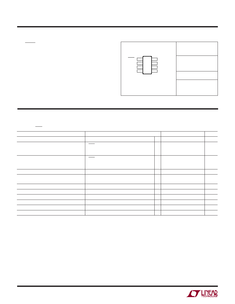
SHDN 1
NC 2
V
IN
3
GND 4
8 FB
7 BIAS
6 BOOST
5 SW
TOP VIEW
TS8 PACKAGE
8-LEAD PLASTIC TSOT-23
ORDER PART
NUMBER
TS8 PART MARKING
T
JMAX
= 125∞C,
JA
= 140∞C/ W
LT3470ETS8
LT3470ITS8
LTBDM
LTBPW
PARAMETER
CONDITIONS
MIN
TYP
MAX
UNITS
Minimum Input Voltage
4
V
Quiescent Current from V
IN
V
SHDN
= 0.2V
0.1
0.5
µA
V
BIAS
= 3V, Not Switching
10
18
µA
V
BIAS
= 0V, Not Switching
35
50
µA
Quiescent Current from Bias
V
SHDN
= 0.2V
0.1
0.5
µA
V
BIAS
= 3V, Not Switching
25
60
µA
V
BIAS
= 0V, Not Switching
0.1
1.5
µA
FB Comparator Trip Voltage
V
FB
Falling
1.228
1.250
1.265
V
FB Pin Bias Current (Note 3)
V
FB
= 1V
35
80
nA
35
150
nA
FB Voltage Line Regulation
4V < V
IN
< 40V
0.0006
0.01
%/V
Minimum Switch Off-Time (Note 5)
500
ns
Switch Leakage Current
0.7
1.5
µA
Switch V
CESAT
I
SW
= 100mA
215
300
mV
Switch Top Current Limit
V
FB
= 0V
250
325
435
mA
Switch Bottom Current Limit
V
FB
= 0V
225
mA
The
denotes specifications which apply over the full operating temperature range, otherwise specifications are T
A
= 25∞C.
V
IN
= 10V, V
SHDN
= 10V, V
BOOST
= 15V, V
BIAS
= 3V unless otherwise specified.
ELECTRICAL CHARACTERISTICS

3
LT3470
3470f
Note 1: Absolute Maximum Ratings are those values beyond which the life
of a device may be impaired.
Note 2: The LT3470E is guaranteed to meet performance specifications
from 0∞C to 70∞C. Specifications over the ≠40∞C to 85∞C operating
temperature range are assured by design, characterization and correlation
with statistical process controls. The LT3470I specifications are
guaranteed over the ≠40∞C to 125∞C temperature range.
PARAMETER
CONDITIONS
MIN
TYP
MAX
UNITS
Catch Schottky Drop
I
SH
= 100mA
630
775
mV
Catch Schottky Reverse Leakage
V
SW
= 10V
0.2
2
µA
Boost Schottky Drop
I
SH
= 30mA
650
775
mV
Boost Schottky Reverse Leakage
V
SW
= 10V, V
BIAS
= 0V
0.2
2
µA
Minimum Boost Voltage (Note 4)
1.7
2.2
V
BOOST Pin Current
I
SW
= 100mA
7
12
mA
SHDN Pin Current
V
SHDN
= 2.5V
1
5
µA
SHDN Input Voltage High
2.5
V
SHDN Input Voltage Low
0.2
V
The
denotes specifications which apply over the full operating temperature range, otherwise specifications are T
A
= 25∞C.
V
IN
= 10V, V
SHDN
= 10V, V
BOOST
= 15V, V
BIAS
= 3V unless otherwise specified.
ELECTRICAL CHARACTERISTICS
Note 3: Bias current flows out of the FB pin.
Note 4: This is the minimum voltage across the boost capacitor needed to
guarantee full saturation of the switch.
Note 5: This parameter is assured by design and correlation with statistical
process controls.
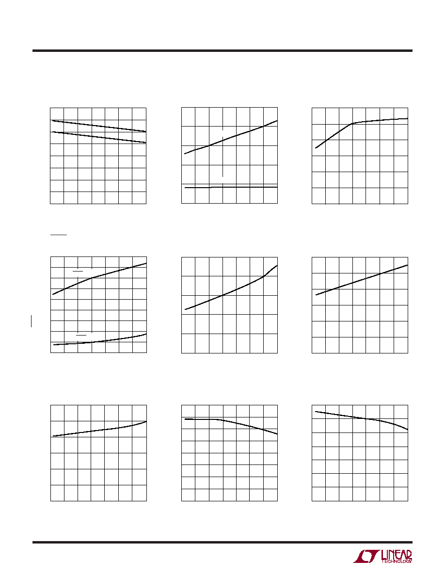
TYPICAL PERFOR A CE CHARACTERISTICS
U
W
Efficiency, V
OUT
= 5V
Efficiency, V
OUT
= 3.3V
V
FB
vs Temperature
LOAD CURRENT (mA)
50
EFFICIENCY (%)
70
90
40
60
80
0.1
10
100
3470 G01
30
1
L = TOKO D52LC 47µH
T
A
= 25∞C
V
IN
= 7V
V
IN
= 12V
V
IN
= 36V
V
IN
= 24V
LOAD CURRENT (mA)
50
EFFICIENCY (%)
70
90
40
60
80
0.1
10
100
3470 G02
30
1
L = TOKO D52LC 47µH
T
A
= 25∞C
V
IN
= 12V
V
IN
= 36V
V
IN
= 24V
TEMPERATURE (∞C)
≠50
1.240
V
FB
(V)
1.245
1.250
1.255
1.260
≠25
0
25
50
3470 G03
75
100
125
4
LT3470
3470f
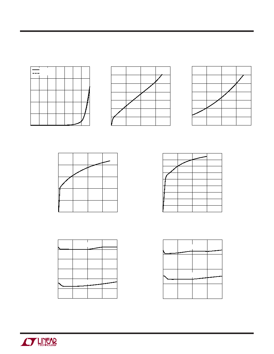
TYPICAL PERFOR A CE CHARACTERISTICS
U
W
V
IN
Quiescent Current
vs Temperature
BIAS Quiescent Current
(Bias > 3V) vs Temperature
SHDN Bias Current
vs Temperature
FB Bias Current (V
FB
= 1V)
vs Temperature
Top and Bottom Switch Current
Limits (V
FB
= 0V) vs Temperature
TEMPERATURE (∞C)
≠ 50
CURRENT LIMIT (mA)
350
25
3470 G04
200
100
≠ 25
0
50
50
0
400
300
250
150
75
100
125
TEMPERATURE (∞C)
≠50
≠25
0
V
IN
CURRENT (
µ
A)
20
50
0
50
75
3470 G05
10
40
30
25
100
125
BIAS < 3V
BIAS > 3V
TEMPERATURE (∞C)
≠50
BIAS CURRENT (
µ
A)
20
25
30
25
75
3470 G06
15
10
≠25
0
50
100
125
5
0
TEMPERATURE (∞C)
≠50
0
SHDN CURRENT (
µ
A)
1
3
4
5
50
9
3470 G07
2
0
≠25
75
100
25
125
6
7
8
V
SHDN
= 36V
V
SHDN
= 2.5V
TEMPERATURE (∞C)
≠50
≠25
0
FB CURRENT (nA)
20
50
0
50
75
3470 G08
10
40
30
25
100
125
FB Bias Current (V
FB
= 0V)
vs Temperature
TEMPERATURE (∞C)
≠50
FB CURRENT (
µ
A)
80
100
120
25
75
3470 G09
60
40
≠25
0
50
100
125
20
0
Switch V
CESAT
(I
SW
= 100mA)
vs Temperature
Boost Diode V
F
(I
F
= 50mA)
vs Temperature
TEMPERATURE (∞C)
≠50
SWITCH V
CESAT
(mV)
200
250
300
25
75
3470 G10
150
100
≠25
0
50
100
125
50
0
TEMPERATURE (∞C)
≠ 50
SCHOTTKY V
F
(V)
0.7
25
3470 G11
0.4
0.2
≠ 25
0
50
0.1
0
0.8
0.6
0.5
0.3
75
100
125
Catch Diode V
F
(I
F
= 100mA)
vs Temperature
TEMPERATURE (∞C)
≠50
0.4
0.5
0.7
25
75
3470 G12
0.3
0.2
≠25
0
50
100
125
0.1
0
0.6
SCHOTTKY V
F
(V)
5
LT3470
3470f
TYPICAL PERFOR A CE CHARACTERISTICS
U
W
Switch V
CESAT
BOOST Pin Current
Catch Diode Forward Voltage
Boost Diode Forward Voltage
Diode Leakage (V
R
= 36V)
vs Temperature
Minimum Input Voltage, V
OUT
= 3.3V
Minimum Input Voltage, V
OUT
= 5V
TEMPERATURE (∞C)
≠50
≠25
0
SCHOTTKY DIODE LEAKAGE (
µ
A)
10
25
0
50
75
3470 G13
5
20
15
25
100
125
BOOST
CATCH
SWITCH CURRENT (mA)
0
400
500
700
300
3470 G14
300
200
100
200
400
100
0
600
SWITCH V
CESAT
(mV)
SWITCH CURRENT (mA)
0
8
10
14
300
3470 G15
6
4
100
200
400
2
0
12
BOOST PIN CURRENT (mA)
CATCH DIODE CURRENT (mA)
0
SCHOTTKY V
F
(V)
0.4
0.6
400
3470 G16
0.2
0
100
200
300
1.0
0.8
BOOST DIODE CURRENT (mA)
0
SCHOTTKY V
F
(V)
500
600
700
200
3470 G17
400
300
0
50
100
150
100
200
900
800
LOAD CURRENT (mA)
0
3.0
INPUT VOLTAGE (V)
3.5
4.0
4.5
5.0
5.5
6.0
50
100
150
200
3470 G18
T
A
= 25∞C
V
IN
TO START
V
IN
TO RUN
LOAD CURRENT (mA)
0
INPUT VOLTAGE (V)
6
7
200
3470 G19
5
4
50
100
150
8
T
A
= 25∞C
V
IN
TO START
V
IN
TO RUN