 | –≠–ª–µ–∫—Ç—Ä–æ–Ω–Ω—ã–π –∫–æ–º–ø–æ–Ω–µ–Ω—Ç: LTC1536 | –°–∫–∞—á–∞—Ç—å:  PDF PDF  ZIP ZIP |

1
LTC2908
sn2908 2908fs
Precision
Six Supply Monitor
Ultralow Voltage Reset: V
CC
= 0.5V Guaranteed*
Monitors Six Inputs Simultaneously:
5V, 3.3V, 2.5V, 1.8V, ADJ1, ADJ2 (LTC2908-A1)
3.3V, 2.5V, 1.8V, 1.5V, ADJ1, ADJ2 (LTC2908-B1)
Guaranteed Threshold Accuracy:
±
1.5% of
Monitored Voltage Over Temperature
Internal V
CC
Auto Select
Power Supply Glitch Immunity
200ms Reset Time Delay
Active Low Open-Drain RST Output
Low Profile (1mm) SOT-23 (ThinSOT
TM
) and Plastic
(2mm ◊ 3mm) DFN Packages
Six Supply Monitor with 5% Tolerance
(12V, 3.3V, 2.5V, 1.8V, 1.5V, 1.2V)
Network Servers
Wireless Base Stations
Optical Networking Systems
Mulitvoltage Systems
Desktop and Notebook Computers
Handheld Devices
FEATURES
DESCRIPTIO
U
APPLICATIO S
U
TYPICAL APPLICATIO
U
The LTC
Æ
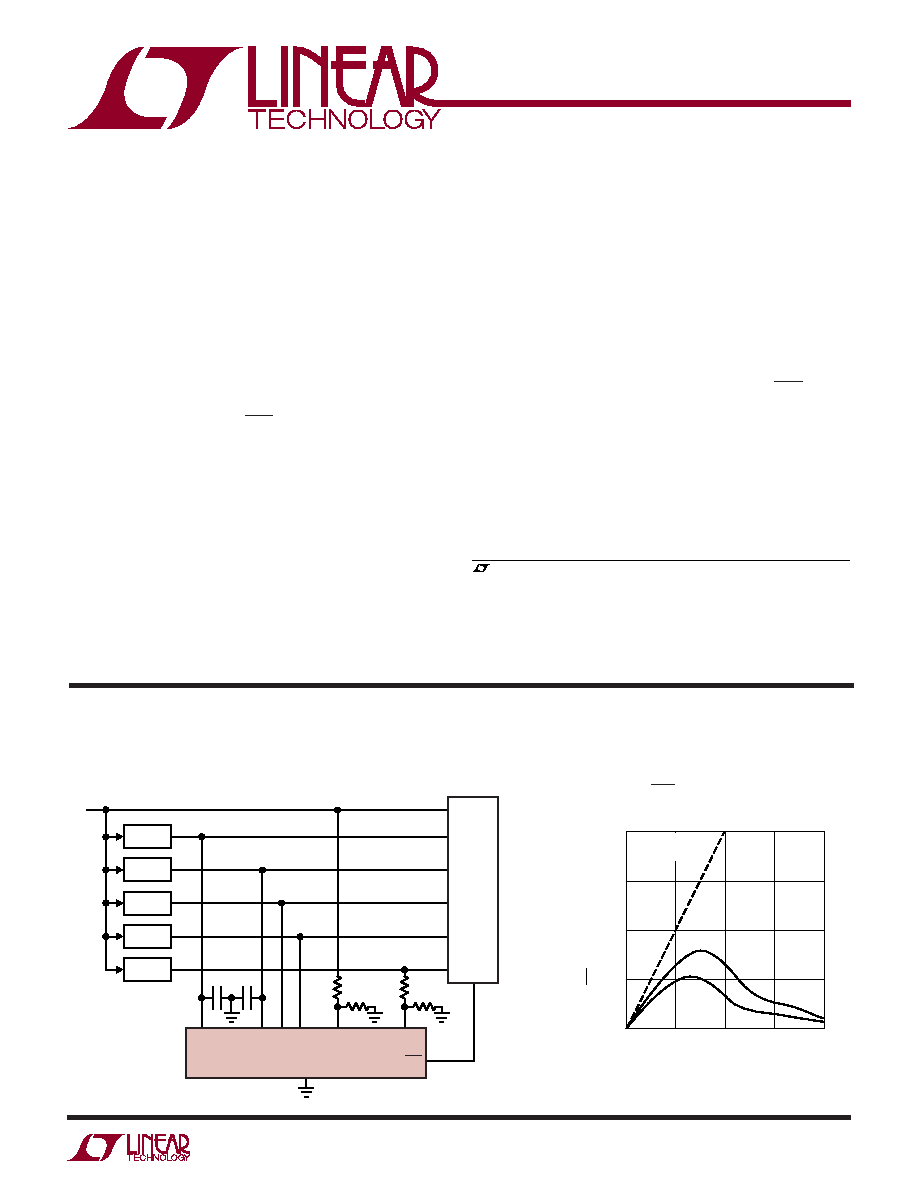
2908 is a six supply monitor for systems with a
large number of supply voltages that require a precise and
compact solution. The common reset output remains low
until all six inputs have been in compliance for 200ms.
The LTC2908 features a tight 1.5% threshold accuracy
over the entire operating temperature range (≠ 40∞C to
85∞C) and glitch immunity to ensure reliable reset opera-
tion without false triggering. The open-drain RST output
state is guaranteed to be in the correct state as long as V1
and/or V2 is 0.5V or greater.
The LTC2908 also features two adjustable inputs with a
nominal threshold level at 0.5V. This product provides a
precise, space-conscious, micropower and general pur-
pose solution for any kind of system requiring supply
monitors.
, LTC and LT are registered trademarks of Linear Technology Corporation.
RST
2.15M
0.1µF
V1
V2 V3 V4
GND
LTC2908-B1
V
ADJ1
12V
3.3V
2.5V
1.8V
1.5V
1.2V
2908 TA01a
0.1µF
100k
DC/DC
DC/DC
DC/DC
DC/DC
DC/DC
SYSTEM
124k
V
ADJ2
100k
V1 (V)
0
RST OUTPUT VOLTAGE (V)
0.2
V2 = GND
V2 = V1
0.3
0.8
2908 TA01b
0.1
0
0.2
0.4
0.6
0.4
V3 = V4 = V
ADJ1
=
V
ADJ2
= GND
RST Output Voltage vs V1
with 10k Pull-Up Resistor to V1
ThinSOT is a trademark of Linear Technology Corporation.
*Patent pending.

2
LTC2908
sn2908 2908fs
Terminal Voltages
V1, V2, V3, V4 ........................................ ≠ 0.3V to 7V
V
ADJ1
, V
ADJ2
........................... ≠ 0.3V to (V
CC
+ 0.3V)
RST ........................................................ ≠ 0.3V to 7V
Operating Temperature Range
LTC2908C-A1/LTC2908C-B1 .................. 0∞C to 70∞C
LTC2908I-A1/LTC2908I-B1 ................ ≠40∞C to 85∞C
ABSOLUTE AXI U RATI GS
W
W
W
U
SYMBOL
PARAMETER
CONDITIONS
MIN
TYP
MAX
UNITS
V
RT50
5V, 5% Reset Threshold
V1 Input Threshold
4.600
4.675
4.750
V
V
RT33
3.3V, 5% Reset Threshold
V2 Input Threshold
3.036
3.086
3.135
V
V
RT25
2.5V, 5% Reset Threshold
V3 Input Threshold
2.300
2.338
2.375
V
V
RT18
1.8V, 5% Reset Threshold
V4 Input Threshold
1.656
1.683
1.710
V
V
RTADJ
ADJ, 5% Reset Threshold
V
ADJ1
, V
ADJ2
Input Threshold
0.492
0.500
0.508
V
(LTC2908-A1) The
denotes specifications which apply over the full
operating temperature range, otherwise specifications are T
A
= 25∞C. V
CC
= 5V, unless otherwise noted. (Note 2)
ELECTRICAL CHARACTERISTICS
(Notes 1, 2)
Consult factory for parts specified with wider operating temperature ranges.
PACKAGE/ORDER I FOR ATIO
U
U
W
LTC2908CTS8-A1
LTC2908ITS8-A1
LTC2908CTS8-B1
LTC2908ITS8-B1
ORDER PART
NUMBER
T
JMAX
= 125∞C,
JA
= 250∞C/ W
Storage Temperature Range
DFN Package .....................................≠65∞C to 125∞C
TSOT-23 Package ..............................≠65∞C to 150∞C
Lead Temperature (Soldering, 10 sec)................. 300∞C
LTBFJ
LTBFK
LTBFM
LTBFN
TS8 PART
MARKING
LTC2908CDDB-A1
LTC2908IDDB-A1
LTC2908CDDB-B1
LTC2908IDDB-B1
ORDER PART
NUMBER
LBFD
LBFF
LBFG
LBFH
DDB8 PART
MARKING
T
JMAX
= 125∞C,
JA
= 76∞C/ W
EXPOSED PAD (PIN 9)
(PCB CONNECTION OPTIONAL)
V2 1
V4 2
RST 3
GND 4
8 V1
7 V
ADJ1
6 V3
5 V
ADJ2
TOP VIEW
TS8 PACKAGE
8-LEAD PLASTIC TSOT-23
TOP VIEW
9
DDB8 PACKAGE
8-LEAD (3mm ◊ 2mm) PLASTIC DFN
5
6
7
8
4
3
2
1
GND
RST
V4
V2
V
ADJ2
V3
V
ADJ1
V1
SYMBOL
PARAMETER
CONDITIONS
MIN
TYP
MAX
UNITS
V
RT33
3.3V, 5% Reset Threshold
V1 Input Threshold
3.036
3.086
3.135
V
V
RT25
2.5V, 5% Reset Threshold
V2 Input Threshold
2.300
2.338
2.375
V
V
RT18
1.8V, 5% Reset Threshold
V3 Input Threshold
1.656
1.683
1.710
V
V
RT15
1.5V, 5% Reset Threshold
V4 Input Threshold
1.380
1.403
1.425
V
V
RTADJ
ADJ, 5% Reset Threshold
V
ADJ1
, V
ADJ2
Input Threshold
0.492
0.500
0.508
V
(LTC2908-B1) The
denotes specifications which apply over the full operating temperature range, otherwise specifications are
T
A
= 25∞C. V
CC
= 3.3V, unless otherwise noted. (Note 2)

3
LTC2908
sn2908 2908fs
SYMBOL
PARAMETER
CONDITIONS
MIN
TYP
MAX
UNITS
V
CC
Internal Operating Voltage
RST in Correct Logic State
0.5
6
V
I
V1
V1 Input Current
V1 = 5.0V (LTC2908-A1) (Note 4)
26
50
µA
V1 = 3.3V (LTC2908-B1)
24
50
µA
I
V2
V2 Input Current
V2 = 3.3V (LTC2908-A1) (Note 4)
10
20
µA
V2 = 2.5V (LTC2908-B1)
8
20
µA
I
V3
V3 Input Current
V3 = 2.5V (LTC2908-A1)
2
5
µA
V3 = 1.8V (LTC2908-B1)
2
5
µA
I
V4
V4 Input Current
V4 = 1.8V (LTC2908-A1)
2
5
µA
V4 = 1.5V (LTC2908-B1)
2
5
µA
I
VADJ
V
ADJ1
, V
ADJ2
Input Current
V
ADJ1
= V
ADJ2
= 0.55V
±15
nA
t
RST
Reset Time-Out Period
160
200
260
ms
t
UV
V
X
Undervoltage Detect to RST or RST
V
X
Less Than Reset Threshold V
RTX
by
250
µs
More Than 1%
V
OH
Output Voltage High RST (Note 5)
I
RST
= ≠1µA, V
CC
= 5V (LTC2908-A1)
V
CC
≠ 1.5
V
I
RST
= ≠1µA, V
CC
= 3.3V (LTC2908-B1)
V
CC
≠ 1.0
V
V
OL
Output Voltage Low RST
V
CC
= 0.5V, I
RST
= 5µA
0.01
0.15
V
V
CC
= 1.0V, I
RST
= 100µA
0.01
0.15
V
V
CC
= 3.0V, I
RST
= 2500µA
0.10
0.30
V
The
denotes specifications which apply over the full operating
temperature range, otherwise specifications are T
A
= 25∞C. V
CC
= 5V for the LT2908-A1 and V
CC
= 3.3V for the LTC2908-B1, unless
otherwise noted. (Notes 2, 3)
ELECTRICAL CHARACTERISTICS
Note 1: Absolute Maximum Ratings are those values beyond which the life
of a device may be impaired.
Note 2: The greater of V1, V2 is the internal supply voltage (V
CC
).
Note 3: All currents into pins are positive; all voltages are referenced to
GND unless otherwise noted.
Note 4: Under typical operating conditions, most of the quiescent current
is drawn from the V1 input. When V2 exceeds V1, V2 supplies most of the
quiescent current.
Note 5: The output pin RST has an internal pull-up to V
CC
of typically 6µA.
However, an external pull-up resistor may be used when a faster rise time
is required or for V
OH
voltages greater than V
CC
.
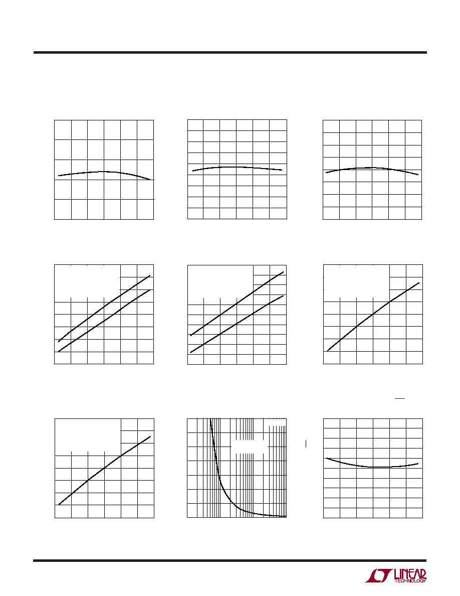
TYPICAL PERFOR A CE CHARACTERISTICS
U
W
5V Threshold Voltage
vs Temperature
3.3V Threshold Voltage
vs Temperature
2.5V Threshold Voltage
vs Temperature
TEMPERATURE (∞C)
≠50
4.750
4.725
4.700
4.675
4.650
4.625
4.600
25
75
2908 G01
≠25
0
50
100
THRESHOLD VOLTAGE, V
RT50
(V)
TEMPERATURE (∞C)
≠50
3.135
3.115
3.095
3.075
3.055
3.035
25
75
2908 G02
≠25
0
50
100
THRESHOLD VOLTAGE, V
RT33
(V)
TEMPERATURE (∞C)
≠50
2.375
2.360
2.345
2.330
2.315
2.300
25
75
2908 G03
≠25
0
50
100
THRESHOLD VOLTAGE, V
RT25
(V)
Specifications are at T
A
= 25∞C unless otherwise noted.

4
LTC2908
sn2908 2908fs
1.8V Threshold Voltage
vs Temperature
1.5V Threshold Voltage
vs Temperature
ADJ Threshold Voltage
vs Temperature
I
V1
vs Temperature
I
V2
vs Temperature
I
V3
vs Temperature
I
V4
vs Temperature
Typical Transient Duration
vs Comparator Overdrive
Reset Time-Out Period (t
RST
)
vs Temperature
TEMPERATURE (∞C)
≠50
1.710
1.700
1.690
1.680
1.670
1.660
25
75
2908 G04
≠25
0
50
100
THRESHOLD VOLTAGE, V
RT18
(V)
TEMPERATURE (∞C)
≠50
THRESHOLD VOLTAGE, V
RT15
(V)
50
1.425
2908 G05
0
≠25
75
25
100
1.410
1.405
1.400
1.395
1.390
1.385
1.380
1.415
1.420
TEMPERATURE (∞C)
≠50
THRESHOLD VOLTAGE, V
RTADJ
(V)
0.4980
0.5000
0.5020
25
75
2908 G06
0.4960
0.4940
0.4920
≠25
0
50
0.5040
0.5060
0.5080
100
TEMPERATURE (∞C)
≠50
I
V1
(
µ
A)
17
19
21
23
29
31
33
27
≠25
0
25
50
2908 G07
75
100
25
A1
B1
V1 = 5.0V (A1)/V1 = 3.3V (B1)
V2 = 3.3V (A1)/V2 = 2.5V (B1)
V3 = 2.5V (A1)/V3 = 1.8V (B1)
V4 = 1.8V (A1)/V4 = 1.5V (B1)
V
ADJ1
= V
ADJ2
= 0.55V
TEMPERATURE (∞C)
≠50
I
V2
(
µ
A)
8
9
A1
B1
10
25
75
2908 G08
7
6
4
5
≠25
0
50
11
12
14
13
100
V1 = 5.0V (A1)/V1 = 3.3V (B1)
V2 = 3.3V (A1)/V2 = 2.5V (B1)
V3 = 2.5V (A1)/V3 = 1.8V (B1)
V4 = 1.8V (A1)/V4 = 1.5V (B1)
V
ADJ1
= V
ADJ2
= 0.55V
TEMPERATURE (∞C)
≠50
I
V3
(
µ
A)
1.7
1.8
1.9
25
75
2908 G09
1.6
1.5
1.4
≠25
0
50
2.0
2.1
2.2
100
V1 = 5.0V (A1)/V1 = 3.3V (B1)
V2 = 3.3V (A1)/V2 = 2.5V (B1)
V3 = 2.5V (A1)/V3 = 1.8V (B1)
V4 = 1.8V (A1)/V4 = 1.5V (B1)
V
ADJ1
= V
ADJ2
= 0.55V
TEMPERATURE (∞C)
≠50
I
V4
(
µ
A)
1.7
1.8
1.9
25
75
2908 G10
1.6
1.5
1.4
≠25
0
50
2.0
2.1
2.2
100
V1 = 5.0V (A1)/V1 = 3.3V (B1)
V2 = 3.3V (A1)/V2 = 2.5V (B1)
V3 = 2.5V (A1)/V3 = 1.8V (B1)
V4 = 1.8V (A1)/V4 = 1.5V (B1)
V
ADJ1
= V
ADJ2
= 0.55V
COMPARATOR OVERDRIVE VOLTAGE (% OF V
RTX
)
0.1
400
TYPICAL TRANSIENT DURATION (
µ
s)
500
600
700
1
10
100
2908 G11
300
200
100
0
RESET OCCURS
ABOVE CURVE
T
A
= 25∞C
TEMPERATURE (∞C)
≠50
RESET TIME-OUT PERIOD, t
RST
(ms)
190
200
210
25
75
2908 G12
180
170
150
160
≠25
0
50
220
230
250
240
100
TYPICAL PERFOR A CE CHARACTERISTICS
U
W
Specifications are at T
A
= 25∞C unless otherwise noted.

5
LTC2908
sn2908 2908fs
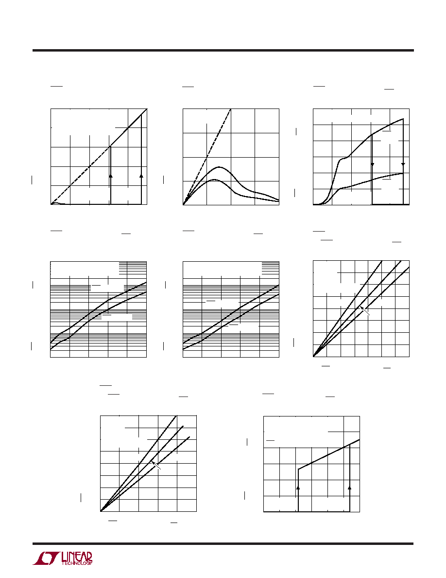
RST Output Voltage vs V1 with
10k Pull-Up Resistor to V1
RST Pull-Down Current (I
RST
)
vs Supply Voltage (V
CC
)
RST Pull-Down Current (I
RST
) vs
Supply Voltage (V
CC
) with Dual
Channel Supply
RST Pull-Up Current (I
RST
)
vs Supply Voltage (V
CC
)
RST Output Voltage vs V1 with
10k Pull-Up Resistor to V1
RST Output Voltage Low (V
OL
)
vs RST Pull-Down Current (I
RST
)
LTC2908-A1
V1 (V)
0
RST OUTPUT VOLTAGE (V)
3.0
4.0
5.0
4
2908 G13
2.0
1.0
0
1
2
3
5
V1 = V2
V3 = 2.5V (A1)/V3 = 1.8V (B1)
V4 = 1.8V (A1)/V4 = 1.5V (B1)
V
ADJ1
= V
ADJ2
= 0.55V
V
RT33
LTC2908-B1
V
RT50
LTC2908-A1
V1 (V)
0
RST OUTPUT VOLTAGE (V)
0.2
V2 = GND
V2 = V1
0.3
0.8
2908 G14
0.1
0
0.2
0.4
0.6
0.4
V3 = V4 = V
ADJ1
=
V
ADJ2
= GND
SUPPLY VOLTAGE, V
CC
(V)
0
RST PULL-DOWN CURRENT, I
RST
(mA)
2
4
1
3
5
6
1
2
3
4
2908 G15
5
0
RST AT
150mV
RST AT
50mV
V
CC
= V1 = V2
V3 = V4 = V
ADJ1
= V
ADJ2
= GND
V
RT33
LTC2908-B1
V
RT50
LTC2908-A1
SUPPLY VOLTAGE, V
CC
(V)
0.01
RST PULL-DOWN CURRENT, I
RST
(mA)
0.1
1
10
0
0.4
0.6
0.8
0.001
0.2
1
2908 G16
V
CC
= V1 = V2
V3 = V4 = V
ADJ1
= V
ADJ2
= GND
RST AT 150mV
RST AT 50mV
RST Pull-Down Current (I
RST
) vs
Supply Voltage (V
CC
) with Single
Channel Supply
SUPPLY VOLTAGE, V
CC
(V)
0.01
RST PULL-DOWN CURRENT, I
RST
(mA)
0.1
1
10
0
0.4
0.6
0.8
0.001
0.2
1
2908 G17
V
CC
= V1
V2 = V3 = V4 = V
ADJ1
= V
ADJ2
= GND
RST AT 150mV
RST AT 50mV
RST PULL-DOWN CURRENT, I
RST
(mA)
0
RST OUTPUT VOLTAGE LOW, V
OL
(V)
0.7
15
2908 G18
0.4
0.2
5
10
20
0.1
0
0.8
0.6
0.5
0.3
25
30
35
V1 = 5.0V
V2 = 3.3V
V3 = 2.5V
V4 = 1.8V
V
ADJ1
= V
ADJ2
= 0.4V
85∞C
≠40∞C
25∞C
RST Output Voltage Low (V
OL
)
vs RST Pull-Down Current (I
RST
)
LTC2908-B1
RST PULL-DOWN CURRENT, I
RST
(mA)
0
RST OUTPUT VOLTAGE LOW, V
OL
(V)
0.7
15
2908 G19
0.4
0.2
5
10
20
0.1
0
0.8
0.6
0.5
0.3
25
V1 = 3.3V
V2 = 2.5V
V3 = 1.8V
V4 = 1.5V
V
ADJ1
= V
ADJ2
= 0.4V
85∞C
≠40∞C
25∞C
SUPPLY VOLTAGE, V
CC
(V)
2
0
RST PULL-UP CURRENT, I
RST
(
µ
A)
≠5
≠10
≠15
≠20
≠30
2.5
3
3.5
4
2908 G20
4.5
5
≠25
V
CC
= V1 = V2
V3 = 2.5V (A1)/V3 = 1.8V (B1)
V4 = 1.8V (A1)/V4 = 1.5V (B1)
V
ADJ1
= V
ADJ2
= 0.55V
RST HELD AT 0V
V
RT33
LTC2908-B1
V
RT50
LTC2908-A1
TYPICAL PERFOR A CE CHARACTERISTICS
U
W
Specifications are at T
A
= 25∞C unless otherwise noted.
