1/10
MP03 XXX 330 Series
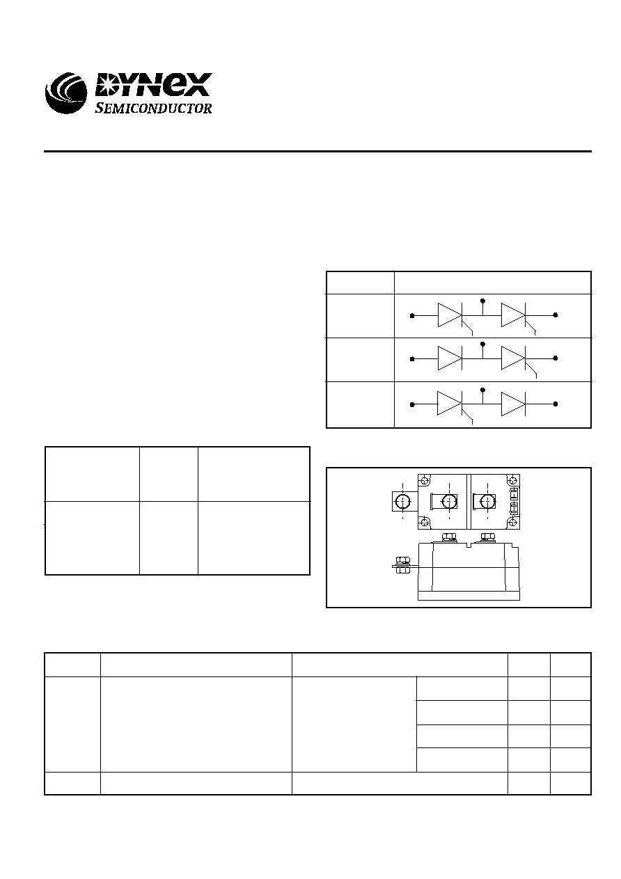
Code
Circuit
HBT
HBP
HBN
MP03/330 - 12
MP03/330 - 10
MP03/330 - 08
Symbol
Max.
Units
334
289
A
A
Conditions
259
A
T
case
= 75
o
C
T
heatsink
= 75
o
C
T
heatsink
= 85
o
C
T
case
= 85
o
C
T
case
= 75
o
C
I
T(RMS)
RMS value
A
223
A
525
Mean on-state current
Halfwave, resistive load
I
T(AV)
1200
1000
800
T
(vj)
= 130
o
C
I
DRM
= I
RRM
= 30mA
V
DSM
& V
RSM
=
V
DRM
& V
RRM
+ 100V
respectively
Module type code: MP03.
See Package Details for further information
FEATURES
s
Dual Device Module
s
Electrically Isolated Package
s
Pressure Contact Construction
s
International Standard Footprint
s
Alumina (non-toxic) Isolation Medium
APPLICATIONS
s
Motor Control
s
Controlled Rectifier Bridges
s
Heater Control
s
AC Phase Control
KEY PARAMETERS
V
DRM
1200V
I
TSM
10600A
I
T(AV)
(per arm)
334A
V
isol
2500V
VOLTAGE RATINGS
Type
Number
Repetitive
Peak
Voltages
V
DRM
V
RRM
CURRENT RATINGS - PER ARM
Parameter
Lower voltage grades available.
For full description of part number see "Ordering instructions"
on page 3.
Conditions
PACKAGE OUTLINE
CIRCUIT OPTIONS
MP03 XXX 330 Series
Phase Control Dual SCR, SCR/Diode Modules
Replaces December 1998 version, DS4483-4.0
DS4483-5.0 January 2000

2/10
MP03 XXX 330 Series
Symbol
Parameter
Conditions
Max.
Units
A
V
R
= 0
V
R
= 50% V
RRM
V
R
= 0
V
R
= 50% V
RRM
A
2
s
10.6
Symbol
Parameter
Conditions
Thermal resistance - case to heatsink
per thyristor or diode
3 phase
Max.
Symbol
Peak reverse and off-state current
From 67% V
DRM
to 600A
Gate source 10V, 5
Rise time 0.5
µ
s, T
j
=130
o
C
r
T
* Higher dV/dt values available, contact factory for particular requirements.
Note 1: The data given in this datasheet with regard to forward voltage drop is for calculation of the power dissipation in the
semiconductor elements only. Forward voltage drops measured at the power terminals of the module will be in excess of these
figures due to the impedance of the busbar from the terminal to the semiconductor.
kA
8.5
0.56 x 10
6
A
2
s
0.36 x 10
6
10ms half sine;
T
j
= 130∞C
10ms half sine;
T
j
= 130∞C
Surge (non-repetitive) on-state current
I
TSM
I
2
t for fusing
I
2
t
dc
Thermal resistance - junction to case
per Thyristor or Diode
halfwave
R
th(j-c)
R
th(c-hs)
Mounting torque = 5Nm
with mounting compound
T
vj
Virtual junction temperature
Off-state (Blocking)
T
stg
Storage temperature range
Commoned terminals to base plate
AC RMS, 1min, 50Hz
Isolation voltage
V
isol
0.11
o
C/W
o
C/W
0.12
2.5
kV
-40 to 130
o
C
o
C
130
0.05
o
C/W
0.13
o
C/W
Units
Conditions
Max.
At 1000A, T
case
= 25
o
C
1.50
V
At V
RRM
/V
DRM
, T
j
= 130
o
C
30
mA
To 67% V
DRM
T
j
= 130
o
C
200*
V/
µ
s
100
A/
µ
s
0.8
V
At T
vj
= 130
o
C
0.7
m
At T
vj
= 130
o
C
On-state slope resistance
V
T(TO)
Threshold voltage
Rate of rise of on-state current
dI/dt
Linear rate of rise of off-state voltage
dV/dt
I
RRM
/I
DRM
On-state voltage
V
TM
THERMAL & MECHANICAL RATINGS
DYNAMIC CHARACTERISTICS- THYRISTOR
SURGE RATINGS - PER ARM
Units
Parameter

3/10
MP03 XXX 330 Series
Symbol
Parameter
Conditions
Gate non-trigger voltage
V
3.0
0.25
Typ.
mA
V
V
GD
Gate trigger voltage
150
V
GT
I
GT
Gate trigger current
At V
DRM
T
case
= 25
o
C
V
DRM
= 5V, T
case
= 25
o
C
V
DRM
= 5V, T
case
= 25
o
C
-
-
-
V
30
0.25
V
V
RGM
Peak reverse gate voltage
V
5.0
-
A
-
-
-
10
I
FGM
Peak forward gate current
Peak forward gate voltage
V
FGM
V
FGN
Peak forward gate voltage
Anode positive with respect to cathode
Anode negative with respect to cathode
Anode positive with respect to cathode
P
GM
P
G(AV)
Peak gate power
Mean gate power
t
p
= 25
µ
s
-
-
100
5
W
W
Max.
Units
s
Adequate heatsinking is required to maintain the base
temperature at 75
o
C if full rated current is to be achieved. Power
dissipation may be calculated by use of V
T(TO)
and r
T
information in
accordance with standard formulae. We can provide assistance
with calculations or choice of heatsink if required.
s
The heatsink surface must be smooth and flat; a surface finish
of N6 (32
µ
in) and a flatness within 0.05mm (0.002") are
recommended.
s
Immediately prior to mounting, the heatsink surface should be
lightly scrubbed with fine emery, Scotch Brite or a mild chemical
etchant and then cleaned with a solvent to remove oxide build up
and foreign material. Care should be taken to ensure no foreign
particles remain.
s
An even coating of thermal compound (eg. Unial) should be
applied to both the heatsink and module mounting surfaces. This
should ideally be 0.05mm (0.002") per surface to ensure optimum
thermal performance.
s
After application of thermal compound, place the module squarely
over the mounting holes, (or 'T' slots) in the heatsink. Using a
torque wrench, slowly tighten the recommended fixing bolts at
each end, rotating each in turn no more than 1/4 of a revolution at
a time. Continue until the required torque of 5Nm (44lb.ins) is
reached at both ends.
s
It is not acceptable to fully tighten one fixing bolt before starting
to tighten the others. Such action may DAMAGE the module.
GATE TRIGGER CHARACTERISTICS AND RATINGS
MOUNTING RECOMMENDATIONS
Examples:
MP03 HBP330 - 08
MP03 HBN330 - 12
MP03 HBT330 - 08
Part number is made up of as follows:
MP03 HBT 330 -10
MP
= Pressure contact module
03
= Outline type
HBT = Circuit configuration code (see "circuit options" - front page)
330
= Nominal average current rating at T
case
= 75
o
C
10
= V
RRM
/100
NOTE: Diode ratings and characteristics are comparable with the SCR in types HBP or HBN
Types HBP or HBN can also be supplied with diode polarity reversed, to special order.
ORDERING INSTRUCTIONS
4/10
MP03 XXX 330 Series
1600
1200
800
400
0
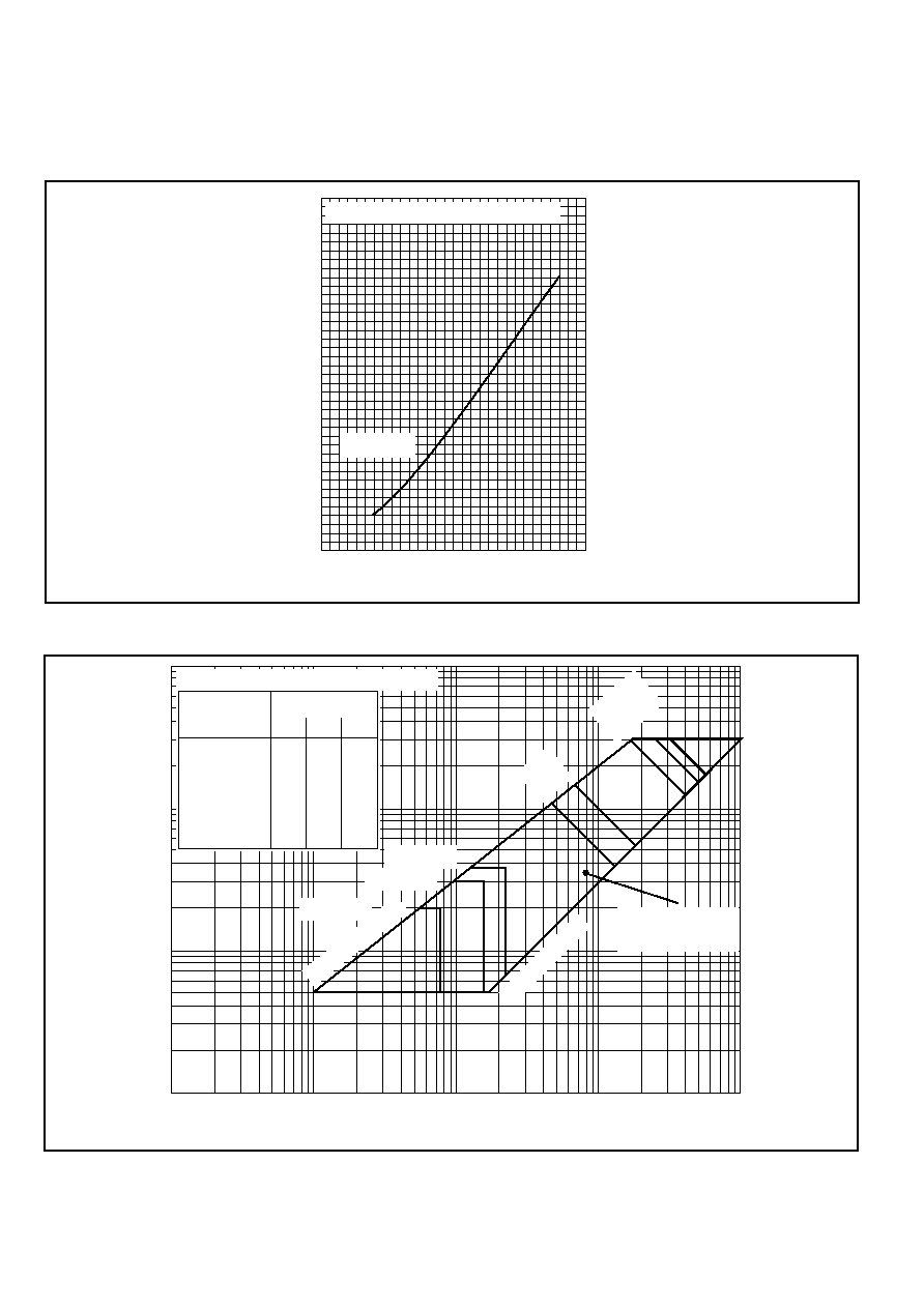
Instantaneous on-state current - (A)
0.6
1.0
1.4
1.8
Instantaneous on-state voltage - (V)
Measured under pulse conditions
T
j
= 130∞C
0.8
1.2
1.6
CURVES
100
10
1
0.1
0.001
0.1
0.01
I
GD
0.1
10
I
FGM
100W
75W
50W
10W
5W
V
FGM
Lower Limit 1%
Upper Limit 99%
T
j
= -40∞C
T
j
= 25∞C
T
j
= 125∞C
Region of
certain triggering
Gate trigger voltage - (V)
Gate trigger current - (A)
FIG 2 GATE CHARACTERISTICS
Table gives pulse power P
GM
in Watts
Pulse Width
µs
20
25
100
500
1ms
10ms
50
100
100
100
100
100
10
100
100
100
100
100
50
-
400
100
100
100
25
-
-
Frequency Hz
Fig. 1 Maximum (limit) on-state characteristics (thyristor or diode) - See Note 1
Fig. 2 Gate trigger characteristics
5/10
MP03 XXX 330 Series
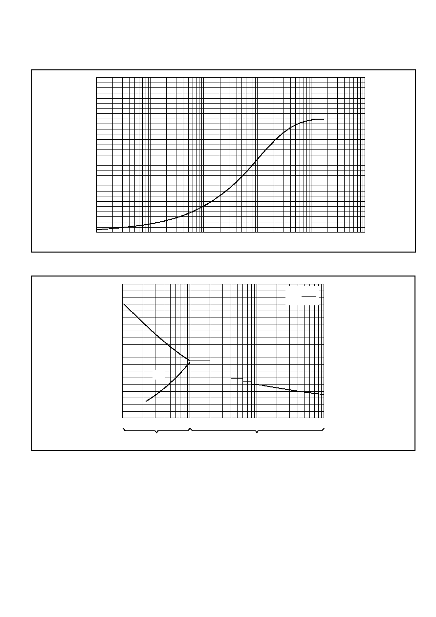
100
10
1.0
0.1
0.01
0.001
Time - (s)
0.15
0
0.10
0.05
Thermal impedance - (∞C/W)
d.c.
20
15
10
5
0
Peak half sine wave on-state current - (kA)
1
10
1
2
3 4 5
50
ms
Cycles at 50Hz
Duration
150
200
250
300
I
2
t value - (A
2
s x 10
3
)
I
2
t
I
2
t = Œ
2
x t
2
350
400
450
500
Fig. 3 Transient thermal impedance (DC) - (Thyristor or diode)
Fig. 4 Surge (non-repetitive) on-state current vs time (with 50% V
RRM
, T
case
= 130∞C (Thyristor or diode)