
1/9
www.dynexsemi.com
MP04DD810
FEATURES
s
Dual Device Module
s
Electrically Isolated Package
s
Pressure Contact Construction
s
International Standard Footprint
s
Alumina (Non-toxic) Isolation Medium
APPLICATIONS
s
Power Supplies
s
Large IGBT Circuit 'Front Ends'
s
Rectifiers
s
Battery Chargers
VOLTAGE RATINGS
KEY PARAMETERS
V
RRM
3000V
I
F(AV)
812A
I
FSM (per arm)
20000A
I
F(RMS)
1276A
V
isol
3000V
3000
2800
2600
2400
MP04DD810-30
MP04DD810-28
MP04DD810-26
MP04DD810-24
Conditions
T
vj
= ≠40∞ to 150∞C,
V
RSM
= V
RRM
+ 100V
Lower voltage grades available
Type Number
Repetitive Peak
Voltages
V
DRM
V
RRM
V
Fig.1 DD circuit configuration
ORDERING INFORMATION
Order As:
MP04DD810-XX-W2
1/4 - 18 NPT connection
MP04DD810-XX-W3
1/4 - 18 NPT connection
MP04DD810-XX-W3A
1/4 - 18 NPT water connection
thread
XX shown in the part number about represents V
DRM
/100
selection required, eg. MP04DD810-28-W2
Note: When ordering, please use the complete part number.
Please quote full part number in all correspondance.
1
2
3
MP04DD810
Dual Rectifier Diode Water Cooled Module
Preliminary Information
DS5286-2.1 June 2001
Fig. 2 Module package variants - (not to scale)
Module outline type code: MP04-W2
(See Package Details for further information)
Module outline type code:
MP04-W3
Module outline type code:
MP04-W3A
2/9
www.dynexsemi.com
MP04DD810
Half wave resistive load
THERMAL AND MECHANICAL DATA
dc, 4.5 Ltr/min
Conditions
Min.
Max.
Units
o
C/W
-
0.106
Halfwave, 4.5 Ltr/min
T
vj
Virtual junction temperature
T
stg
Storage temperature range
-
Thermal resistance - junction to water
(per diode)
R
th(j-w)
Symbol
Parameter
Screw torque
6 (53)
-
Nm (lb.ins)
≠40
150
o
C
Reverse (blocking)
-
150
o
C
3 Phase, 4.5 Ltr/min
-
0.112
o
C/W
-
0.102
o
C/W
Symbol
Parameter
Conditions
I
F(AV)
Mean forward current
I
F(RMS)
RMS value
Units
Max.
885
A
T
water (in)
= 40
o
C
812
A
T
water (in)
= 25
o
C, 4.5 Ltr/min
1392
A
T
water (in)
= 40
o
C, 4.5 Ltr/min
1276
A
ABSOLUTE MAXIMUM RATINGS - PER ARM
Stresses above those listed under 'Absolute Maximum Ratings' may cause permanent damage to the device. This is a stress rating
only and functional operation of the device at these or any other conditions above those indicated in the operational sections of this
specification is not implied. Exposure to Absolute Maximum Ratings for extended periods may affect device reliability.
T
water (in)
= 25
o
C
10ms half sine; T
j
= 150
o
C
V
R
= 0
10ms half sine; T
j
= 150
o
C
V
R
= 50% V
RRM
I
FSM
Surge (non-repetitive) forward current
I
2
t
I
2
t for fusing
I
FSM
Surge (non-repetitive) forward current
I
2
t
I
2
t for fusing
1.28 x 10
6
A
2
s
16
kA
2.0 x 10
6
A
2
s
20
kA
V
isol
Isolation voltage
3000
V
Commoned terminals to base plate AC RMS, 1 min, 50Hz
Mounting - M6
-
-
12 (106) Nm (lb.ins)
Electrical connections - M10
-
Refer to
Drawing
g
-
-
Weight (nominal)
4.5 Ltr/min

3/9
www.dynexsemi.com
MP04DD810
Note 1:
The data given in this datasheet with regard to forward voltage drop is the for the calculation of the power dissipation in
the semiconductor elements only. Forward voltage drops measured at the power terminals will be in excess of these figures due to
the impedance of the busbars from the terminals to the semiconductor.
CHARACTERISTICS
Peak reverse current
Parameter
µ
C
1600
At T
vj
= 150∞C
-
Q
S
Total stored charge
I
F
= 1000A, dI
RR
/dt = 3A/
µ
s
T
case
= 150∞C, V
R
= 100V
Symbol
I
RRM
I
RR
Peak recovery current
V
TO
Threshold voltage. See Note 1.
r
T
Slope resistance. See Note 1.
0.29
m
At T
vj
= 150∞C
-
0.7
V
-
85
A
-
At V
RRM
, T
case
= 150
o
C
-
50
mA
Conditions
Min.
Max.
Units

4/9
www.dynexsemi.com
MP04DD810
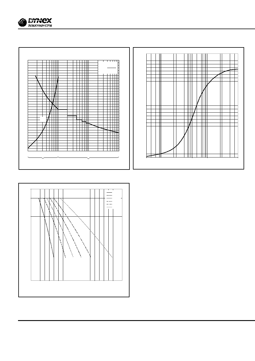
Fig.5 Maximum stored charge
0.1
1.0
10
100
Rate of decay of on-state current dI
F
/dt - (A/µs)
10000
1000
100
Stored charge Q
S
- (µ
C)
Conditions:
T
j
= 150∞C
V
R
= 100V
I
F
= 1000A
I
RR
I
F
dI
F
/dt
Q
S
Fig.6 Maximum reverse recovery current
1.0
10
100
Rate of decay of forward current dI
F
/dt - (A/µs)
1000
100
10
Reverse current I
RR
- (A)
Conditions:
T
j
= 150∞C
V
R
= 100V
I
F
= 1000A
CURVES
Fig.3 Maximum (limit) forward characteristics
0.5
0.75
1.0
1.5
1.25
Instantaneous forward voltage V
F
- (V)
0
500
1000
1500
2000
2500
Instantaneous forward current I
F
- (A)
Measured under pulse
conditions
T
j
= 25∞C
T
j
= 150∞C
Fig.4 Power dissipation curves
0
200
400
600
800
1000
1200
1400
1600
1800
2000
2200
0
200
400
600
800
1000 1200 1400 1600 1800
Forward current, (Average, per arm) I
F(AV)
- (A)
Power dissipation (Watts, per arm)
30∞
60∞
90∞
120∞
180∞
DC
5/9
www.dynexsemi.com
MP04DD810
Fig.7 Surge (non-repetitive) forward current vs time
(with 50% V
RRM
@ T
c
- 150∞C)
1
10
1
2
3
5
10 20
50
0
5
10
15
20
25
30
35
0.8
0.9
0.7
1.0
1.1
I
2
t value - (A
2
s x 10
6
)
ms
Cycles at 50Hz
Duration
Peak half sine forward current - (kA)
I
2
t = Œ
2
x t
2
1.2
1.3
I
2
t
1.4
Fig.8 Transient thermal impedance - dc
0
0.02
0.04
0.06
0.08
0.1
0.12
0.001
0.01
0.1
1
10
100
1000
Time (Seconds)
Thermal resistance, Junction to water, R
th(j-w)
- (
∞
C/W)
Fig. 9 Maximum permissible water inlet temperature vs on-state
current at specified conduction angles, sine wave 50/60Hz
0
10
20
30
40
50
60
70
80
90
100
100
200
300
400
500
600
700
800
900 1000 1100
Forward current (Average, per arm), I
F(AV)
- (A)
Maximum permissble inlet water temperature - (
∞
C)
30∞
60∞
90∞
120∞
180∞
DC