 | –≠–ª–µ–∫—Ç—Ä–æ–Ω–Ω—ã–π –∫–æ–º–ø–æ–Ω–µ–Ω—Ç: SD5401CY | –°–∫–∞—á–∞—Ç—å:  PDF PDF  ZIP ZIP |

Linear Integrated Systems, Inc. 4042 Clipper Ct. Fremont, CA 94538 Tel: 510 490-9160 Fax: 510 353-0261
1
High-Speed DMOS FET Analog Switches and Switch Arrays
Introduction
This Application Note describes in detail the
principle of operation of the SD210/5000 series
of high-speed analog switches and switch
arrays. It contains an explanation of the most
important switch characteristics, application
examples, test data, and other application hints.
Description
The Linear Systems SD210 and SD5000 series
are discretes and quad monolithic arrays,
respectively, of single-pole single-throw analog
switches. These switches are n-channel
enhancement-mode silicon field effect
transistors built using double-diffusion MOS
(DMOS) silicon gate technology. Surface-
mount versions (SST211, SD5400 Series) are
also available.
This family of devices is designed to handle a
wide variety of video, fast ATE, and telecom
analog switching applications. They are capable
of ultrafast switching speeds (t
r
= 1 ns, t
OFF
= 3
ns) and excellent transient response. Thanks to
the reduced parasitic capacitances, DMOS can
handle wideband signals with high off-isolation
and minimum crosstalk.
The SD210 series of single-channel FETs is
produced without Zener protection to reduce
leakage and in Zener protected versions to
reduce electrostatic discharge hazards. The
SD5000 series is available in 16-lead dual in-
line surface mount or sidebraze ceramic
packages. Analog signal voltage ranges up to
±10 V and frequencies up to 1 GHz can be
controlled.
For surface-mount applications the SST211
series is offered in the TO-253 (SOT-143)
package. The SD5400 series comes in the
narrow body gull-wing SO-14 package.
Applications
Fast switching speeds, low on-state resistance,
high channel-to-channel isolation, low
capacitance, and low charge injection make
these DMOS devices especially well suited for a
variety of applications.
A few of the many possible application areas for
DMOS analog switches are as follows:
1. Video and RF switching (high speed, high off-
isolation, low crosstalk):
-Multiple video distribution networks
-Sampling scanners for RF systems
2. Audio routing (glitch- and noise-free):
-High-speed switching
-Audio switching systems using
digitized remote control
3. Data acquisition (highspeed, low charge
injection, low leakage):
-High-speed sample-and-holds
-Audio and communication A/D
converters
4. Other:
-Digital switching
-PCM distribution networks
-UHF Amplifiers
-VHF Modulators and Double-Balanced
Mixers
-High-speed inverters/drivers
-Switched capacitor filters
-Choppers
Linear Integrated Systems, Inc. 4042 Clipper Ct. Fremont, CA 94538 Tel: 510 490-9160 Fax: 510 353-0261
2
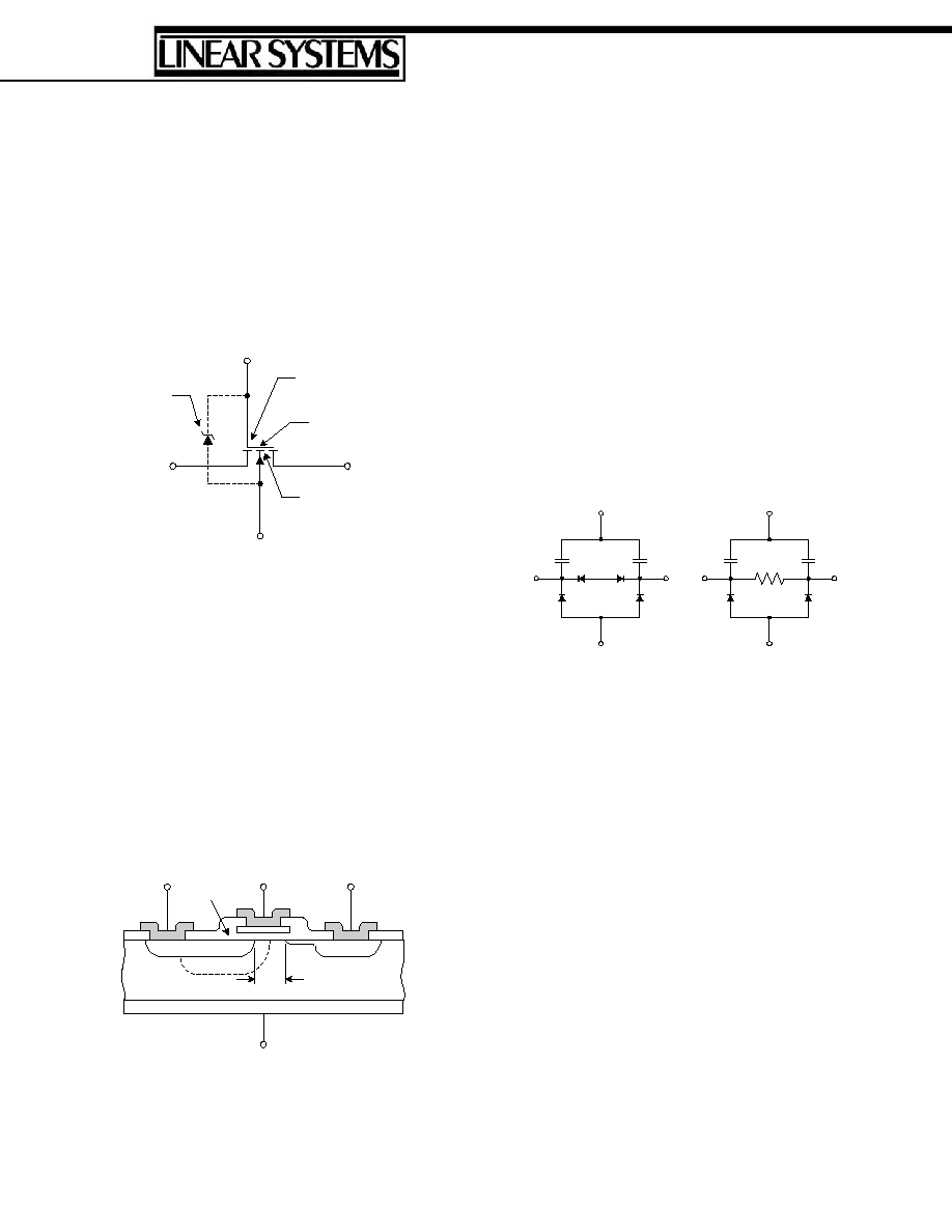
Principle of Operation
Figure 1 depicts an n-channel enhancement-
mode device with an insulated gate and
asymmetrical structure. The gate protection
Zener is shown with broken lines to indicate
that, although it is present on the chip, it is not a
main constituent of the fundamental switch
structure.
The DMOS field-effect transistor (FET) is
normally off when the gate-to-source voltage
(V
GS
) is 0 V. The lateral DMOS transistor,
shown in cross-section in Figure 2, has three
terminals (source, gate, and drain) on the top
surface and one (the body or substrate) on the
bottom. A Zener diode with a breakdown
voltage of approximately 40 V is added to
protect the gate against overvoltage and
electrostatic discharges.
The double-diffusion process creates a thin self-
aligning region of p-type material, isolating the
source from the drain region. The very short
channel length that results between the two
junction depths produces extremely low source-
to-drain and gate-to-drain capacitances at the
same time that it provides good breakdown
voltages.
When the gate potential is equal to or negative
with respect to the source, the switch is off. In
this state, the p-type material in the channel
forms two back-to-back diodes and prevents
channel conduction (Figure 3a). If a voltage is
applied between the S and D regions, only a
small junction leakage current will flow.
The silicon oxide insulation present between
gate and source forms a small capacitor that
accumulates charge.
If the gate-to-source potential (V
GS
) is made
positive, the capacitive effect attracts electrons
to the channel area immediately adjacent to gate
oxide. As V
GS
increases, the electron density in
the channel will exceed the hole density, and the
channel will become an n-type region. As the
channel conductivity is enhanced, the n-n-n
structure becomes a simple silicon resistor
through which current can easily flow in either
direction.
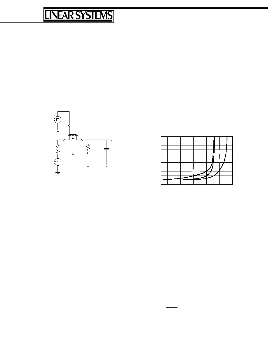
Figure 4 shows typical biasing for ±10 V analog
signal processing. Note that the drain is
Asymmetrical
Structure
Insulated
Gate
Protection
Zener
Enhancement
Mode n-Channel
Source
Body
Drain
Gate
Figure 1. DMOS Electrical System
Source
Gate
Drain
Body
Oxide
Channel
n+
p-
p
n+
Figure 2. Cross Sectional View of an Idealized
DMOS Structure
G
C
GD
C
GS
+
D
S
B
G
C
GD
D
S
B
C
GS
+
r
DS(on)
Figure 3. Equivalent Circuits
(b) On State
(a) Off State
Linear Integrated Systems, Inc. 4042 Clipper Ct. Fremont, CA 94538 Tel: 510 490-9160 Fax: 510 353-0261
3
recommended for the output. Since C
GD
< C
GS
this causes less charge injection noise on the
load.
As can be seen from Figures 3a and 3b, the
body-source and body-drain pn junctions should
be kept reverse biased at all times-otherwise,
signal clipping and even device damage may
occur if unlimited currents are allowed to flow.
Body biasing is conveniently set, in most cases,
by connecting the substrate to V-.
Main Switch Characteristics
r
DS(on)
Channel on-resistance is controlled by the
electric field present across and along the
channel. Channel resistance is mainly
determined by the gate-to-source voltage
difference. When V
GS
exceeds the threshold
voltage (V
GS(th)
), the FET starts to turn on.
Numerous applications call for switching a point
to ground. In these cases the source and
substrate are connected to ground and a gate
voltage of 3 to 4 V is sufficient to ensure
switching action.
With a V
GS
in excess of +5 V, a low resistance
path exists between the source and the drain.
The circuit shown in Figure 4 exhibits the r
DS(on)
vs. analog signal voltage relationship shown in
Figure 5.
When the analog signal excursion is large (for
example ±10 V) the channel on-resistance
changes as a function of signal level. To
achieve minimum distortion, this channel on-
resistance modulation should be kept in mind,
and the amount of resistance in series with the
switch should be properly sized. For instance, if
the switch resistance varies between 20 and
30 over the signal range and the switch is in
series with a 200 load, the result will be a
total R = 4.5 %. Whereas, if the load is 100
k, R will only be 0.01 %.
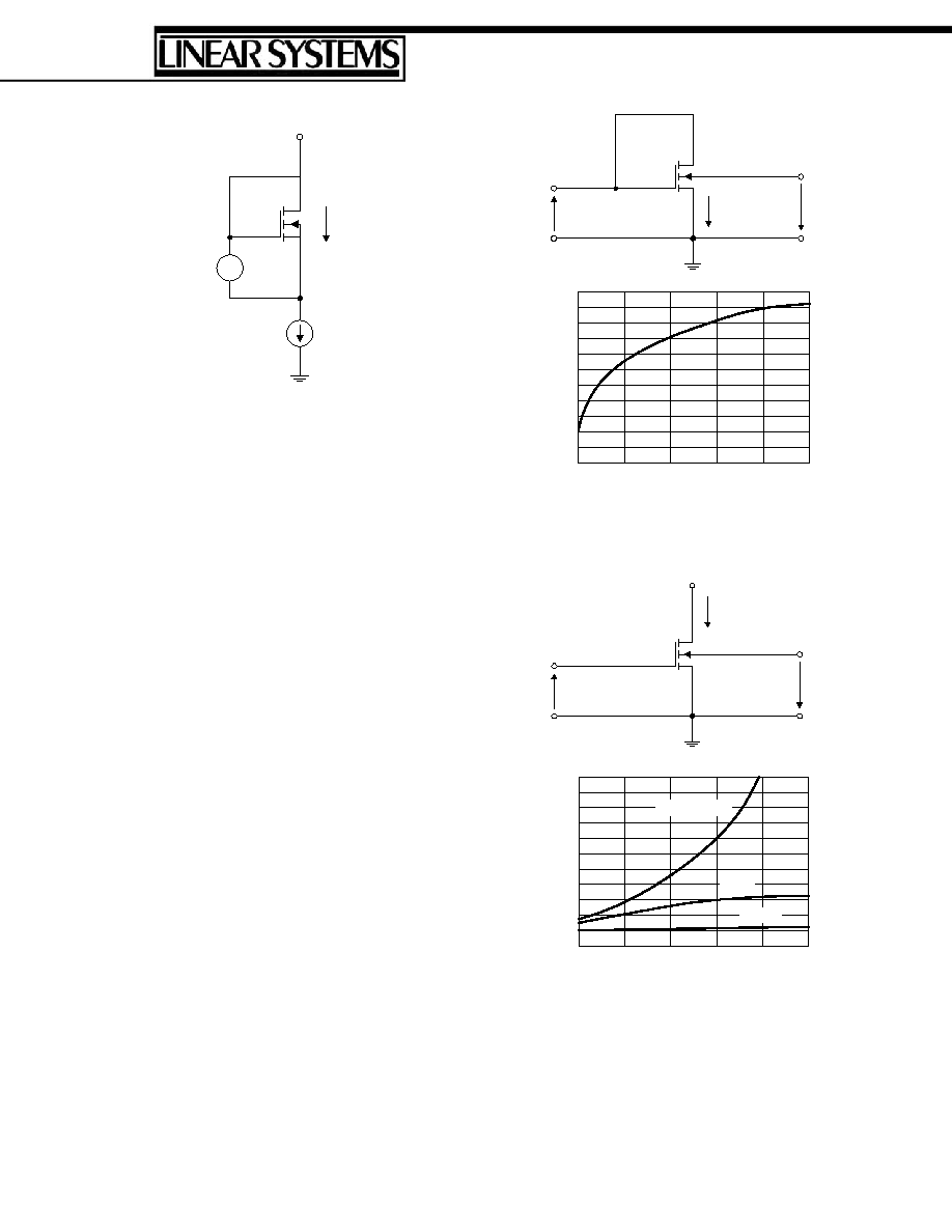
Threshold Voltage
The threshold voltage (V
GS(th)
) is a parameter
used to describe how much voltage is needed to
initiate channel conduction. Figure 6 shows the
applicable test configuration. In this circuit, it is
worth noting, for instance, that if the device has
a V
GS(th)
= 0.5 V, when V+ = 0.5 V, the channel
resistance will be:
500k
A
1
0.5V
R
CHANNEL
=
=
µ
R
GEN
R
L
C
L
G
D
B
S
V
O
-10 V
20 V = On
-10 V = Off
Switch Input
V
S
= ±10 V
Switch
Output
Control
Input
Figure 4. Normal Switch Configuration for a ±10
V Analog Switch
200
160
120
80
40
0
-10
-5
0
5
10
15
V
S
(V)
r
DS(on
)
(
)
(a)
(b)
(c)
(a) V
BODY
= -10 V, V
GATE
= 20 V
(b) V
BODY
= -10 V, V
GATE
= 15 V
(c) V
BODY
= 0 V, V
GATE
= 20 V
Figure 5. On Resistance Characteristics
Linear Integrated Systems, Inc. 4042 Clipper Ct. Fremont, CA 94538 Tel: 510 490-9160 Fax: 510 353-0261
4
Body Effect
For a MOSFET with a uniformly doped
substrate, the threshold voltage is proportional
to the square root of the applied source-to-body
voltage. The SD5000 family has a non-uniform
substrate, and the V
GS(th)
behaves somewhat
differently. Figure 7 shows the typical V
GS(th)
variation as a function of the source-to-body
voltage VSB.
As the body voltage increases in the negative
direction, the threshold goes up. Consequently,
if V
GS
is small, the on-resistance of the channel
can be very high. Figure 8 shows the effects of
V
SB
and V
GS
on r
DS(on)
. Therefore, to maintain a
low on-resistance it is preferable to bias the
body to a voltage close to the negative peaks of
V
S
and use a gate voltage as high as possible.
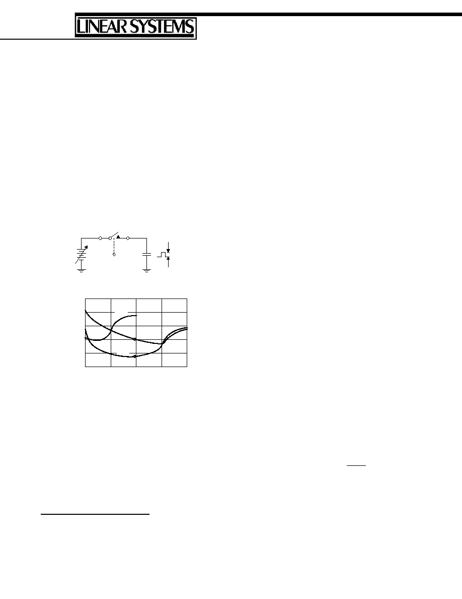
Charge Injection
Charge injection describes that phenomenon by
which a voltage excursion at the gate produces
an injection of electric charges via the gate-to-
drain and the gate-to-source capacitances into
the analog signal path. Another popular name
for this phenomenon is "switching spikes."
V
GS(th)
1µA
V+
Figure 6. Threshold Voltage Test Configuration
V
GS(th)
1µA
V
SB
D
S
3.0
2.5
2.0
1.5
1.0
0.5
0
4
8
12
16
20
V
SB
(V)
V
GS
(t
h
)
(V)
Figure 7. Threshold vs Source to Body Voltage
V
GS
V
SB
D
S
1mA
V
D
300
240
180
120
60
0
0
4
8
12
16
20
V
SB
(V)
r
DS(
o
n
)
(
)
V
GS
= 4 V
5 V
10 V
Figure 8. On Resistance vs Source to Body and
Gate to Source Voltages
Linear Integrated Systems, Inc. 4042 Clipper Ct. Fremont, CA 94538 Tel: 510 490-9160 Fax: 510 353-0261
5
Since these DMOS devices are asymmetrical
1
,
the charge injected into the S and D terminals is
different. Typical parasitic capacitances are on
the order of 0.2 pF for C
DG
and 1.5 pF for C
SG
.
Another factor that influences the amount of
charge injected is the amplitude of the gate-
voltage excursion. This is a directly
proportional relationship: the larger the
excursion, the larger the injected charge. This
can be seen by comparing curves (a) and (c) in
Figure 9. One other variable to consider is the
rate of gate-voltage change. Large amounts of
charge are injected when faster rise and fall
times are present at the gate. This is shown by
curves (a) and (b) in Figure 9.
Switching spikes occur at switch turn-on as well
as turn-off time. When the switch turns on, the
charge injection effect is minimized by the
usually low signal-source impedance. This low
1
The chip geometry is such that non-identical behavior
occurs when the source and drain terminals are reversed
in a circuit.
impedance tends to produce a rapid decay of the
extra charge introduced in the channel. At turn-
off, however, the injected charge might become
stored in a sampling capacitor and create offsets
and errors. These errors will have a magnitude
that is inversely proportional to the magnitude
of the holding capacitance.
Figure 9 illustrates several typical charge
injection characteristics. Figure 10 shows some
of the corresponding waveforms. The DMOS
FETs, because of their inherent low parasitic
capacitances, produce very low charge injection
when compared to other analog switches
(PMOS, CMOS, JFET, BIFET etc.). Still, when
the offsets created are unacceptable, charge
injection compensation techniques exist that
eliminate or minimize them. The solution
basically consists of injecting another charge of
equal amplitude but opposite polarity at the time
when the switch turns off.
Off-Isolation and Crosstalk
The dc on-state resistance is typically 30 and
the off-state resistance is typically 10
10
,
which results in an off-state to on-state
resistance ratio in excess of 10
8
. However, for
video and VHF switching applications, the
upper usable frequency limit is determined by
how much of the incoming signal is coupled
through the parasitic capacitances and appears at
the switch outputwhen ideally no signal
should appear there in the off state.
Off-Isolation is defined by the formula:
IN
OUT
V
V
20log
(dB)
Isolation
-
Off
=
When several analog switches are
simultaneously being used to control high
frequency signals, crosstalk becomes a very
important characteristic. For video applications,
the stray signal coupled via parasitic
D
C
H
Q = C
H
x
V
S
G
V
0
-2
-4
-6
-8
-10
-10
-5
0
5
10
V
S
(V)
Q (p
C
)
(1)
(2)
(c)
(b)
(a)
(a) V
G
= 10 V, t
f
= 0.3 V/µs
(b) V
G
= 10 V, t
f
= 0.03 V/µs
(c) V
G
= 0, -10 V, t
f
= 0.3 V/µs
Figure 9. SD5000 Charge Injection