 | –≠–ª–µ–∫—Ç—Ä–æ–Ω–Ω—ã–π –∫–æ–º–ø–æ–Ω–µ–Ω—Ç: LND339 | –°–∫–∞—á–∞—Ç—å:  PDF PDF  ZIP ZIP |
LND339
Quadruple Differential Comparators
DATA SHEET
GENERAL DESCRIPTION
∑ Wide supply voltage range
(5 to 30V
DC
or
± 2.5 to ± 15V
DC
)
∑ Very low supply current drain(0.8mA)-
independent of supply voltage
∑ Low input biasing current: (25nA)
∑ Low input offset current(±5nA)
∑ Offset
voltage(
±2mV)
∑ Input common-mode voltage range
includes GND
∑ Differential input voltage range equal
to the power supply voltage
∑ Output voltage compatible with
TTL,DTL ECL MOS and CMOS logic
systems.
FEATURES
The LND339 consists of four independent
precision voltage comparators with an offset
voltage as low as 2mV max for all four
comparators, designed specifically to operate
from a single power supply over a wide range of
voltages. These comparators also have a unique
characteristic in that the input common-mode
voltage range includes ground, even though
operated from a single power supply voltage.
Operation from split power supplies is also
possible and the low power supply current drain
is independent of the magnitude of the power
supply voltage.
Application areas include limit comparators,
simple analog to digital converters, pulse,
squarewave and time delay generators: wide
range VCO, MOS clock timers: multi vibrators
and high voltage digital logic gates. The LND339
was designed to directly interface with TTL and
CMOS. When the LND339 series is operated
from both plus and minus power supplies, it will
directly interface with MOS logic where their low
power drain is a distinct advantage over
standard comparators.
ADVANTAGES
∑ High precision comparators
∑ Reduced V
OS
drift over temperature
∑ Power drain suitable for battery operation
∑ Allows sensing near ground
∑ Compatible with all forms of logic
∑ Eliminates need for dual supplies
∑ Linear Dimensions, Inc. ∑ 445 East Ohio Street, Chicago IL 60611 USA ∑ tel 312.321.1810 ∑ fax 312.321.1830 ∑
www.lineardimensions.com
∑

Parameter
Test Conditions
Min
Typ
Max
Unit
25
∞C
2
5
V
IO
Input offset voltage
V
CC
=5V to 30V
V
IC
=V
ICR
min
, V
O
=1.4V
Full range*
9
mV
25
∞C
5
50
I
IO
Input offset current
V
O
=1.4V
Full range*
150
nA
25
∞C
25
250
I
IB
Input bias current
V
O
=1.4V
Full range*
400
nA
25
∞C
0
V
ICR
Common-mode input
voltage range**
Full
Range*
0
V
CC
-1.5
V
CC
- 2
V
A
VD
Large-signal differential
voltage amplification
V
CC =
15V
V
O
=1.4V to 11.4 V,
R
L
15k
25
∞C
50
200
V/mV
V
OH =
5V, V
ID =
1V
25
∞C
0.1
50
nA
I
OH
High-level output current
V
OH =
30V, V
ID
=1V
Full
Range*
1
µA
25
∞C
150
400
mV
V
OL
Low-Level output voltage
I
OL
=4mA, V
ID
=-1V
Full
Range*
700
mV
I
OL
Low-level output current
V
OL=
1.5V,V
ID
=-1V
25
∞C
6
16
mA
V
CC
=5V
25
∞C
0.8
2
mA
I
CC
Supply current
R
L
=
V
CC=
30V
Full
Range*
2.5
mA
*Full range (MIN to Max), for the LND339 is 0
∞C to 70∞C. All characteristics are measured with zero common-mode
input voltage unless otherwise specified.
**The voltage at either input or common-mode should not be allowed to go negative by more than 0.3V. The upper
end of the common-mode voltage range is V
CC
-1.5V, but either or both inputs can go to 30V without damage.
Parameter
Test Conditions
Min
Typ Max
Unit
100-mV input step with 5-mV
overdrive
1.3
Response time
R
L
connected to 5V
through 5.1 k
,
C
L=
15pF*(see Note
1)
TTL-level input step
0.3
µs
*C
L
includes probe and jig capacitance.
Note 1: The response time specified is the interval between the input step function and the instant when the output
crosses 1.4V.
ELECTRICAL CHARACTERISTICS
LND339
SWITCHING CHARACTERISTICS
∑ Linear Dimensions, Inc. ∑ 445 East Ohio Street, Chicago IL 60611 USA ∑ tel 312.321.1810 ∑ fax 312.321.1830 ∑
www.lineardimensions.com
∑
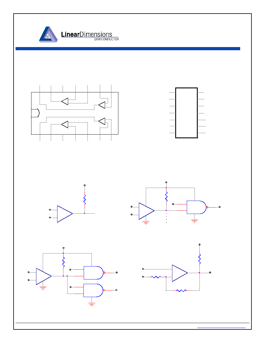
PIN CONFIGURATION
1
2
3
4
5
6
7
8
9
10
11
12
13
14
1
2
3
4
+
+
+
+
-
-
-
-
OUTPUT 2 OUTPUT 1
V+
INPUT 1- INPUT 1+ INPUT 2- INPUT 2+
OUTPUT 3
OUTPUT 4
GND INPUT 4+ INPUT 4- INPUT 3+ INPUT 3-
1
14
2
3
4
11
12
13
OUTPUT 2
INPUT 1-
OUTPUT 4
6
7
5
10
9
8
OUTPUT 1
V+
INPUT 1+
INPUT 2-
INPUT 2+
INPUT 4+
INPUT 4-
INPUT 3+
INPUT 3-
GND
OUTPUT 3
LM139W
SOME TYPICAL APPLICATIONS
1/4LND139
V
V+
+V
+V
IN
REF
+
-
BASIC COMPARATOR
3.0 K
1/4LND139
+5.0 V
+
-
DC
DRIVING CMOS
3
12
100 K
1
2
3
+5.0 V
-
1/4LND139
+
DC
DRIVING TTL
12
3
10 K
1
2
3
1
2
3
V
O
V+
+V
IN
REF
+
-
NON INVERTING COMPARATOR
WITH HYSTERESIS
1/4LND139
+V
3.0 K
10K
10M
(V+=5.0 Vdc)
∑ Linear Dimensions, Inc. ∑ 445 East Ohio Street, Chicago IL 60611 USA ∑ tel 312.321.1810 ∑ fax 312.321.1830 ∑
www.lineardimensions.com
∑
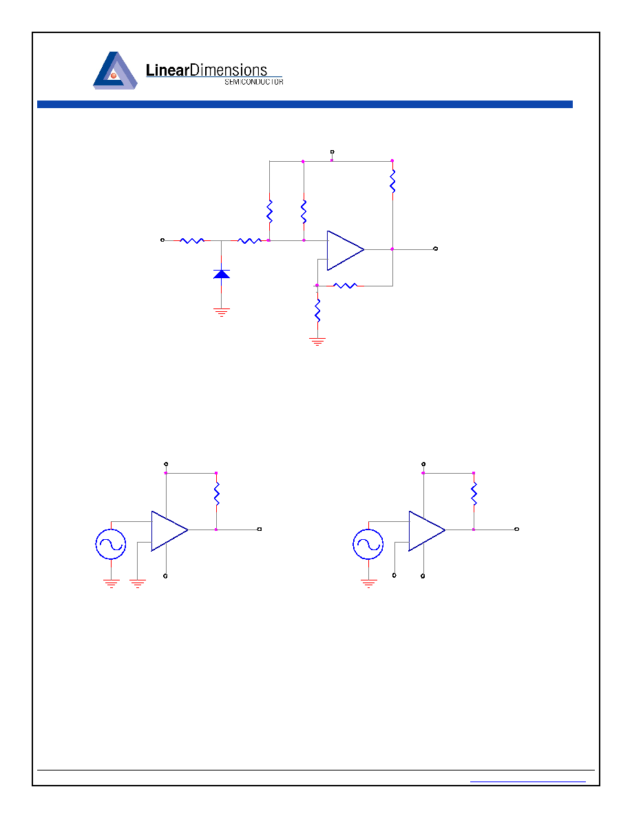
LND339
LND339

LND339
V+
-
V
+V
INVERTING COMPARATOR
WITH HYSTERESIS
O
IN
+
1/4LND139
V+
3.0 K
1M
1M
1M
1/4LND139
V+ (12 Vdc)
+
-
LIMIT COMPARATOR
-
+
IN
+V
1/4LND139
REF LOW
+V
+V
REF HI
S
2R
S
2R
R
S
10.0 K
1
2
LAMP
1
2
1/4LND139
V
O
V+
+
-
V+
SQUAREWAVE OSCILLATOR
0
V+
f 100kHz
4.3K
100K
100K
100K
100K
75 pF
1/4 LND139
V+
+
-
+15 Vdc
V
O
D1
D2
R1
R2
*
* For Large Raios of R1/R2, D1 can be
omitted.
t0t1 t2
6 s
µ
60 s
µ
0
V+
PULSE GENERATOR
15k
1M
1M
1M
1M
80 pF
100k
∑ Linear Dimensions, Inc. ∑ 445 East Ohio Street, Chicago IL 60611 USA ∑ tel 312.321.1810 ∑ fax 312.321.1830 ∑
www.lineardimensions.com
∑
LND339
-
V+
+
1/4 LND139
ZERO DETECTOR CROSSING
(SINGLE POWER SUPPLY)
V
IN
V
O
5.1k
10k
20M
5.1k
5.1k
100k
100k
SPLIT SUPPLY APPLICATIONS
V+
1/4 LND139
V
O
3
+
-
V-
12
ZERO CROSSING DETECTOR
+
V
IN
5.1k
1
2
V
O
V+
1/4 LND139
3
+
-
V-
12
COMPARATOR WITH A NEGATIVE REFERENCE
-5 Vdc
+
V
IN
5.1k
1
2
∑ Linear Dimensions, Inc. ∑ 445 East Ohio Street, Chicago IL 60611 USA ∑ tel 312.321.1810 ∑ fax 312.321.1830 ∑
www.lineardimensions.com
∑