 | –≠–ª–µ–∫—Ç—Ä–æ–Ω–Ω—ã–π –∫–æ–º–ø–æ–Ω–µ–Ω—Ç: 317B | –°–∫–∞—á–∞—Ç—å:  PDF PDF  ZIP ZIP |
1
LT1317/LT1317B
Micropower, 600kHz PWM
DC/DC Converters
DESCRIPTIO
N
U
FEATURES
The LT
Æ
1317/LT1317B are micropower, fixed frequency
step-up DC/DC converters that operate over a wide input
voltage range of 1.5V to 12V. The LT1317 features auto-
matic shifting to power saving Burst Mode
TM
operation at
light loads. High efficiency is maintained over a broad
300
µ
A to 200mA load range. Peak switch current during
Burst Mode operation is kept below 250mA for most
operating conditions which results in low output ripple
voltage, even at high input voltages. The LT1317B does
not shift into Burst Mode operation at light loads, eliminat-
ing low frequency output ripple at the expense of light load
efficiency.
The LT1317/LT1317B contain an internal low-battery de-
tector with a 200mV reference that stays alive when the
device goes into shutdown.
No-load quiescent current of the LT1317 is 100
µ
A and
shuts down to 30
µ
A. The internal NPN power switch
handles a 500mA current with a voltage drop of just
300mV.
The LT1317/LT1317B are available in MS8 and SO-8
packages.
s
100
µ
A Quiescent Current
s
Operates with V
IN
as Low as 1.5V
s
600kHz Fixed Frequency Operation
s
Starts into Full Load
s
Low-Battery Detector Active in Shutdown
s
Automatic Burst Mode Operation at
Light Load (LT1317)
s
Continuous Switching at Light Loads (LT1317B)
s
Low V
CESAT
Switch: 300mV at 500mA
s
Pin for Pin Compatible with the LT1307/LT1307B
s
Cellular Telephones
s
Cordless Telephones
s
Pagers
s
GPS Receivers
s
Battery Backup
s
Portable Electronic Equipment
s
Glucose Meters
s
Diagnostic Medical Instrumentation
APPLICATIO
N
S
U
Burst Mode is a trademark of Linear Technology Corporation.
, LTC and LT are registered trademarks of Linear Technology Corporation.
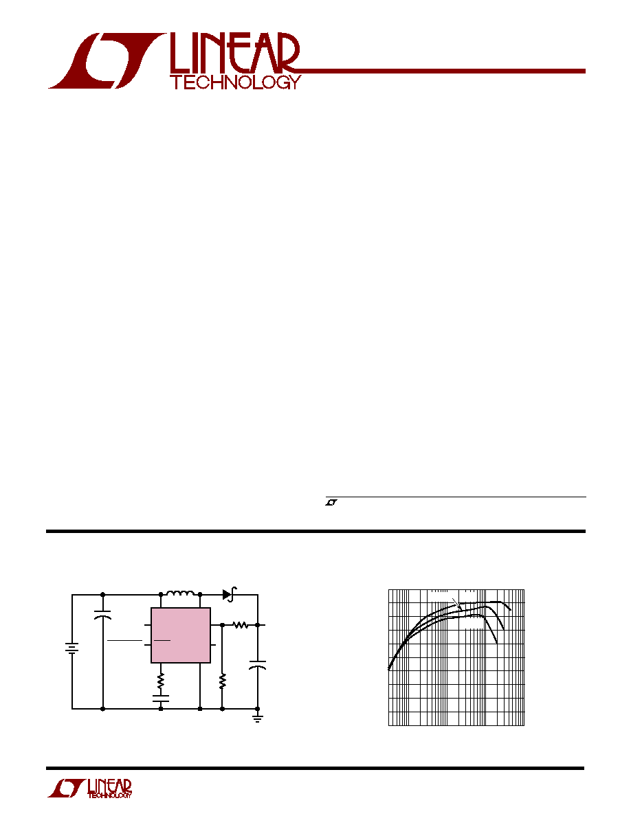
TYPICAL APPLICATIO
N
U
Figure 1. 2-Cell to 3.3V Boost Converter
V
IN
SW
FB
LT1317
L1
10
µ
H
D1
LBO
LBI
SHDN
SHUTDOWN
R
C
33k
R2*
604k
1%
3.3V
200mA
R1
1M
1%
C
C
3.3nF
1317 F01
C1
47
µ
F
C2
47
µ
F
2
CELLS
D1: MBR0520
L1: SUMIDA CD43-100
* FOR 5V OUTPUT, R2 = 332k, 1%
V
C
GND
+
+
2-Cell to 3.3V Converter Efficiency
LOAD CURRENT (mA)
50
EFFICIENCY (%)
60
70
80
90
0.3
10
100
1000
1317 TA01
40
1
3V
IN
1.65V
IN
2.2V
IN
2
LT1317/LT1317B
ORDER PART
NUMBER
A
U
G
W
A
W
U
W
A
R
BSOLUTE
XI
TI
S
V
IN
, LBO Voltage ..................................................... 12V
SW Voltage ............................................... ≠ 0.4V to 30V
FB Voltage .................................................... V
IN
+ 0.3V
V
C
Voltage ................................................................ 2V
LBI Voltage ............................................ 0V
V
LBI
1V
SHDN Voltage ............................................................ 6V
Junction Temperature .......................................... 125
∞
C
Operating Temperature Range
Commercial ........................................... 0
∞
C to 70
∞
C
Industrial ............................................ ≠ 40
∞
C to 85
∞
C
Storage Temperature Range ................ ≠ 65
∞
C to 150
∞
C
Lead Temperature (Soldering, 10 sec)................ 300
∞
C
W
U
U
PACKAGE/ORDER I FOR ATIO
ORDER PART
NUMBER
1
2
3
4
V
C
FB
SHDN
GND
8
7
6
5
LBO
LBI
V
IN
SW
TOP VIEW
MS8 PACKAGE
8-LEAD PLASTIC MSOP
T
JMAX
= 125
∞
C,
JA
= 160
∞
C/W
1
2
3
4
8
7
6
5
TOP VIEW
LBO
LBI
V
IN
SW
V
C
FB
SHDN
GND
S8 PACKAGE
8-LEAD PLASTIC SO
T
JMAX
= 125
∞
C,
JA
= 120
∞
C/W
SYMBOL
PARAMETER
CONDITIONS
MIN
TYP
MAX
UNITS
I
Q
Quiescent Current
Not Switching, V
SHDN
= 2V (LT1317)
q
100
160
µ
A
V
SHDN
= 0V (LT1317/LT1317B)
q
25
40
µ
A
V
SHDN
= 2V, Switching (LT1317B)
4.8
6.5
mA
V
SHDN
= 2V, Switching (LT1317B)
q
7.5
mA
V
FB
Feedback Voltage
1.22
1.24
1.26
V
q
1.20
1.24
1.26
V
I
B
FB Pin Bias Current (Note 2)
q
12
60
nA
Input Voltage Range
q
1.5
12
V
g
m
Error Amp Transconductance
I = 5
µ
A
q
70
140
240
µ
mhos
A
V
Error Amp Voltage Gain
700
V/V
Maximum Duty Cycle
q
80
85
%
Switch Current Limit (Note 3)
V
IN
= 2.5V, Duty Cycle = 30%
710
800
1300
mA
V
IN
= 2.5V, Duty Cycle = 30%
q
660
1350
mA
Burst Mode Operation Switch Current Limit
Duty Cycle = 30% (LT1317)
275
mA
f
OSC
Switching Frequency
q
520
620
720
kHz
ELECTRICAL C
C
HARA TERISTICS
Commercial Grade
V
IN
= 2V, V
SHDN
= 2V, T
A
= 25
∞
C, unless otherwise noted.
Consult factory for Military grade parts.
MS8 PART MARKING
S8 PART MARKING
LT1317CS8
LT1317BCS8
LT1317IS8
LT1317BIS8
1317
1317B
1317I
1317BI
LTHA
LTHB
LT1317CMS8
LT1317BCMS8
(Note 1)
3
LT1317/LT1317B
ELECTRICAL C
C
HARA TERISTICS
Commercial Grade
V
IN
= 2V, V
SHDN
= 2V, T
A
= 25
∞
C unless otherwise noted.
Industrial Grade
V
IN
= 2V, V
SHDN
= 2V, ≠ 40
∞
C
T
A
85
∞
C unless otherwise noted.
SYMBOL
PARAMETER
CONDITIONS
MIN
TYP
MAX
UNITS
I
Q
Quiescent Current
Not Switching, V
SHDN
= 2V (LT1317)
q
160
µ
A
V
SHDN
= 0V (LT1317/LT1317B)
q
40
µ
A
V
SHDN
= 2V, Switching (LT1317B)
q
7.5
mA
V
FB
Feedback Voltage
q
1.20
1.26
V
I
B
FB Pin Bias Current (Note 2)
q
80
nA
Input Voltage Range
q
1.7
12
V
g
m
Error Amp Transconductance
I = 5
µ
A
q
70
140
240
µ
mhos
Maximum Duty Cycle
q
80
%
Switch Current Limit (Note 3)
V
IN
= 2.5V, Duty Cycle = 30%
q
550
1350
mA
f
OSC
Switching Frequency
q
500
750
kHz
Shutdown Pin Current
V
SHDN
= V
IN
q
0.1
µ
A
V
SHDN
= 0V
q
≠ 7
µ
A
LBI Threshold Voltage
q
180
220
mV
LBO Output Low
I
SINK
= 10
µ
A
q
0.25
V
LBO Leakage Current
V
LBI
= 250mV, V
LBO
= 5V
q
0.1
µ
A
LBI Input Bias Current (Note 4)
V
LBI
= 150mV
q
60
nA
Switch Leakage Current
V
SW
= 5V
q
3
µ
A
Switch V
CE
Sat
I
SW
= 500mA
q
400
mV
Reference Line Regulation
1.8V
V
IN
12V
q
0.15
%/V
SHDN Input Voltage High
q
1.4
6
V
SHDN Input Voltage Low
q
0.4
V
SYMBOL
PARAMETER
CONDITIONS
MIN
TYP
MAX
UNITS
Shutdown Pin Current
V
SHDN
= V
IN
q
0.015
0.06
µ
A
V
SHDN
= 0V
q
≠ 2.3
≠ 6
µ
A
LBI Threshold Voltage
190
200
210
mV
q
180
200
220
mV
LBO Output Low
I
SINK
= 10
µ
A
q
0.15
0.25
V
LBO Leakage Current
V
LBI
= 250mV, V
LBO
= 5V
q
0.02
0.1
µ
A
LBI Input Bias Current (Note 4)
V
LBI
= 150mV
q
5
40
nA
Low-Battery Detector Gain
1M
Load
2000
V/V
Switch Leakage Current
V
SW
= 5V
q
0.01
3
µ
A
Switch V
CE
Sat
I
SW
= 500mA
300
350
mV
q
400
mV
Reference Line Regulation
1.8V
V
IN
12V
q
0.08
0.15
%/V
SHDN Input Voltage High
q
1.4
6
V
SHDN Input Voltage Low
q
0.4
V
Note 2: Bias current flows into FB pin.
Note 3: Switch current limit guaranteed by design and/or correlation to
static tests. Duty cycle affects current limit due to ramp generator.
Note 4: Bias current flows out of LBI pin.
The
q
denotes specifications which apply over the full operating
temperature range.
Note 1: Absolute Maximum Ratings are those values beyond which the life
of a device may be impaired.
4
LT1317/LT1317B
TYPICAL PERFOR A CE CHARACTERISTICS
U
W
INPUT VOLTAGE
0
OSCILLATOR FREQUENCY (kHz)
700
650
600
550
500
2
4
6
8
1317 TPC01
10
12
25
∞
C
≠40
∞
C
85
∞
C
Oscillator Frequency
DUTY CYCLE (%)
0
20
40
60
80
100
SWITCH CURRENT (mA)
1317 TPC02
800
600
400
200
0
V
IN
= 2V
L = 10
µ
H
Burst Mode Current Limit (LT1317)
Switch Current Limit,
Duty Cycle = 30%
SWITCH CURRENT (A)
0
0.2
0.4
0.6
0.8
1
SWITCH VOLTAGE (V
CESAT
) (mV)
1317 TPC06
700
600
500
400
300
200
100
0
25
∞
C
≠40
∞
C
85
∞
C
Switch Voltage Drop (V
CESAT
)
TEMPERATURE (
∞
C)
≠50
0
50
≠25
25
75
100
LBI INPUT BIAS CURRENT (nA)
1317 TPC05
6
5
4
3
2
1
0
LBI Input Bias Current
Switch Current Limit
TEMPERATURE (
∞
C)
≠50
≠25
QUIESCENT CURRENT (
µ
A)
1317 TPC09
110
100
90
80
70
60
50
40
30
0
25
50
75
100
Quiescent Current, SHDN = 2V
TEMPERATURE (
∞
C)
≠50
FEEDBACK VOLTAGE (V)
1.25
1.24
1.23
1.22
1.21
1.20
≠25
0
25
50
1317 TPC07
75
100
Feedback Voltage
TEMPERATURE (
∞
C)
≠50
LBI REFERENCE VOLTAGE (mV)
1317 TPC08
203
202
201
200
199
198
197
196
195
≠25
0
25
50
75
100
LBI Reference Voltage
TEMPERATURE (
∞
C)
≠50
SWITCH CURRENT (mA)
1000
900
800
700
600
500
≠25
0
25
50
1317 TPC03
75
100
DUTY CYCLE (%)
0
SWITCH CURRENT (mA)
1200
1000
800
600
400
200
20
40
60
80
1317 TPC04
100
MINIMUM (25
∞
C)
TYPICAL
5
LT1317/LT1317B
TYPICAL PERFOR A CE CHARACTERISTICS
U
W
TEMPERATURE (
∞
C)
≠50
QUIESCENT CURRENT (
µ
A)
26
25
24
23
22
21
20
≠25
0
25
50
1317 TPC10
75
100
TEMPERATURE (
∞
C)
≠50
≠25
0
25
50
75
100
FB PIN BIAS CURRENT (nA)
1317 TPC11
40
36
32
28
24
20
16
12
8
4
0
Quiescent Current, SHDN = 0V
FB Pin Bias Current
SHDN Pin Current
LOAD CURRENT (mA)
1
EFFICIENCY (%)
90
80
70
60
50
40
10
100
1000
1317 TPC14
V
IN
= 3V
V
IN
= 2.2V
V
IN
= 1.65V
LOAD CURRENT (mA)
1
EFFICIENCY (%)
90
80
70
60
50
40
10
100
1000
1317 TPC15
V
IN
= 3V
V
IN
= 2.2V
V
IN
= 1.65V
LOAD CURRENT (mA)
EFFICIENCY (%)
90
80
70
60
50
10
100
1000
1317 TPC13
1
0.3
V
IN
= 3V
V
IN
= 2.2V
V
IN
= 1.65V
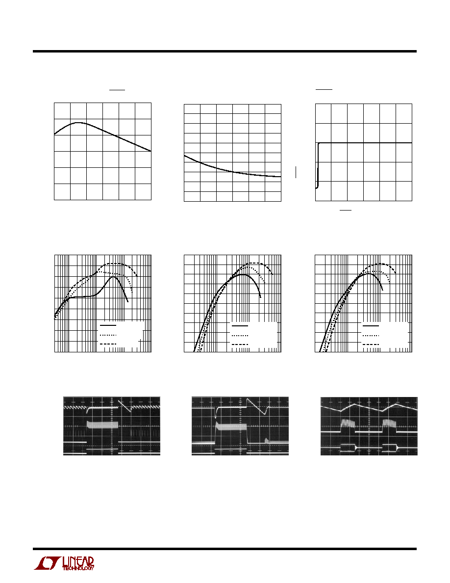
5V Output Efficiency, Circuit of
Figure 1 (LT1317)
2-Cell to 3.3V Converter
Efficiency (LT1317B)
2-Cell to 5V Converter Efficiency
(LT1317B)
Burst Mode Operation (LT1317)
V
OUT
50mV/DIV
AC COUPLED
I
L
200mA/DIV
V
SW
5V/DIV
V
IN
= 2V
20
µ
s/DIV
1317 TPC18
V
OUT
= 3.3V
I
LOAD
= 30mA
CIRCUIT OF FIGURE 1
Transient Response (LT1317B)
V
OUT
100mV/DIV
AC COUPLED
I
L
200mA/DIV
V
IN
= 2V
1ms/DIV
1317 TPC17
V
OUT
= 3.3V
CIRCUIT OF FIGURE 1
WITH LT1317B
Transient Response (LT1317)
V
OUT
100mV/DIV
AC COUPLED
I
L
200mA/DIV
V
IN
= 2V
1ms/DIV
1317 TPC16
V
OUT
= 3.3V
CIRCUIT OF FIGURE 1
I
LOAD
165mA
5mA
I
LOAD
165mA
5mA
SHDN PIN VOLTAGE (V)
0
SHDN PIN CURRENT (
µ
A)
3
5
1317 TPC12
1
2
4
2
1
0
≠1
≠2
≠3
6