 | –≠–ª–µ–∫—Ç—Ä–æ–Ω–Ω—ã–π –∫–æ–º–ø–æ–Ω–µ–Ω—Ç: 3433IFE | –°–∫–∞—á–∞—Ç—å:  PDF PDF  ZIP ZIP |
1
LT3433
3433ia
High Voltage
Step-Up/Step-Down
DC/DC Converter
September 2003
s
Automatic Step-Up and Step-Down Conversion
s
Uses a Single Inductor
s
Wide 4V to 60V Input Voltage Range
s
V
OUT
from 3.3V to 20V
s
Dual Internal 500mA Switches
s
100
µ
A No-Load Quiescent Current
s
Low Current Shutdown
s
±
1% Output Voltage Accuracy
s
200kHz Operating Frequency
s
Boosted Supply Pin to Saturate High Side Switch
s
Frequency Foldback Protection
s
Current Limit Foldback Protection
s
Current Limit Unaffected by Duty Cycle
s
16-lead Thermally Enhanced TSSOP Package
s
12V Automotive Systems
s
Wall Adapter Powered Systems
s
Battery Power Voltage Buffering
, LTC and LT are registered trademarks of Linear Technology Corporation.
FEATURES
DESCRIPTIO
N
U
APPLICATIO S
U
TYPICAL APPLICATIO
U
Burst Mode is a registered trademark of Linear Technology Corporation.
The LT
Æ
3433 is a 200kHz fixed-frequency current mode
switching regulator that provides both step-up and step-
down regulation using a single inductor. The IC operates
over a 4V to 60V input voltage range making it suitable for
use in various wide input voltage range applications such
as automotive electronics that must withstand both load
dump and cold crank conditions.
Internal control circuitry monitors system conditions and
converts from single switch buck operation to dual switch
bridged operation when required, seamlessly changing
between step-down and step-up voltage conversion.
Optional Burst Mode
Æ
operation reduces no-load quies-
cent current to 100
µ
A and maintains high efficiencies with
light loads.
Current limit foldback and frequency foldback help pre-
vent inductor current runaway during start-up. Program-
mable soft-start helps prevent output overshoot at start-up.
The LT3433 is available in a 16-lead thermally enhanced
TSSOP package.
V
BST
SW_H
V
IN
BURST_EN
V
C
V
FB
SW_L
PWRGND
V
OUT
V
BIAS
SHDN
SS
SGND
LT3433
1N4148
0.1
µ
F
68k
100k
0.5%
305k
0.5%
1nF100pF
2.2
µ
F
V
IN
4V TO 60V
0.01
µ
F
3433 TA01
0.1
µ
F
1N4148
L1
100
µ
H
CoEv DU1352-101M
B120A
47
µ
F
V
OUT
5V
4V
V
IN
8.5V: 125mA
8.5V
V
IN
60V: 350mA
+
B160A
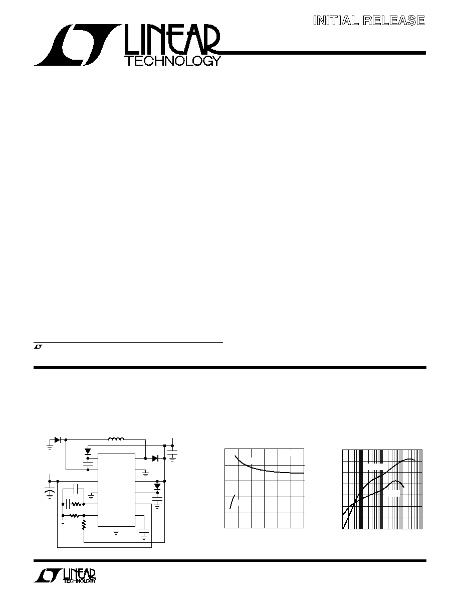
4V to 60V to 5V DC/DC Converter
with Burst Mode Operation
Final Electrical Specifications
Information furnished by Linear Technology Corporation is believed to be accurate and reliable.
However, no responsibility is assumed for its use. Linear Technology Corporation makes no represen-
tation that the interconnection of its circuits as described herein will not infringe on existing patent rights.
OUTPUT CURRENT (mA)
40
EFFICIENCY (%)
60
80
90
0.1
10
100
1000
3433 TA01b
20
1
70
50
30
V
IN
= 13.8V
V
IN
= 4V
Efficiency
V
IN
(V)
0
0
MAXIMUM OUTPUT CURRENT (mA)
100
200
300
400
500
10
20
30
40
3433 TA01c
50
60
BRIDGED
BUCK
V
OUT
= 5V
Maximum Output
Current vs V
IN

2
LT3433
3433ia
SYMBOL
PARAMETER
CONDITIONS
MIN
TYP
MAX
UNITS
V
IN
Operating Voltage Range
q
4
60
V
V
IN(UVLO)
Undervoltage Lockout
Enable Threshold
q
3.4
3.95
V
Undervoltage Lockout Hysteresis
160
mV
V
OUT
Operating Voltage Range
q
3.3
20
V
V
BST
Operating Voltage Range
V
BST
< V
SW_H
+ 20V
q
75
V
V
BST
≠ V
SW_H
q
3.3
20
V
I
VIN
Normal Operation
(Notes 2, 3)
q
580
940
µ
A
Burst Mode Operation
V
VC
< 0.6V
q
100
190
µ
A
Shutdown
V
SHDN
< 0.4V
q
10
25
µ
A
V
BIAS
Internal Supply Output Voltage
q
2.6
2.9
V
Operating Voltage Range
q
20
V
I
VBIAS
Normal Operation
q
660
990
µ
A
Burst Mode Operation
V
VC
< 0.6V
0.1
µ
A
Shutdown
V
SHDN
< 0.4V
0.1
µ
A
Short-Circuit Current Limit
4.5
mA
R
SWH(ON)
Boost Supply Switch On-Resistance
I
SW
= 500mA
q
0.8
1.2
R
SWL(ON)
Output Supply Switch On-Resistance
I
SW
= 500mA
q
0.6
1
V
SHDN
Shutdown Pin Thresholds
Disable
q
0.4
V
Enable
q
1
V
I
VBST
/I
SW
Boost Supply Switch Drive Current
High Side Switch On, I
SW
= 500mA
q
30
50
mA/A
I
VOUT
/I
SW
Output Supply Switch Drive Current
Low Side Switch On, I
SW
= 500mA
q
30
50
mA/A
I
LIM
Switch Current Limit
q
0.5
0.7
0.9
A
Foldback Current Limit
V
FB
= 0V
0.35
A
I
SS
Soft-Start Output Current
q
3
5
9
µ
A
V
FB
Feedback Reference Voltage
1.224
1.231
1.238
V
q
1.215
1.245
V
(Note 1)
Input Supply (V
IN
) .................................... ≠0.3V to 60V
Boosted Supply (V
BST
) .............. ≠0.3V to V
SW_H
+ 30V
(V
BST(MAX)
= 80V)
Internal Supply (V
BIAS
) ............................. ≠ 0.3V to 30V
SW_H Switch Voltage .................................. ≠ 2V to 60V
SW_L Switch Voltage ............................... ≠ 0.3V to 30V
Feedback Voltage (V
FB
) ............................... ≠ 0.3V to 5V
Operating Junction Temperature Range (Note 5)
LT3433E (Note 6) ............................ ≠ 40
∞
C to 125
∞
C
LT3433I ........................................... ≠ 40
∞
C to 125
∞
C
Storage Temperature Range ................ ≠ 65
∞
C to 150
∞
C
Lead Temperature (Soldering, 10 sec)................. 300
∞
C
ABSOLUTE
M
AXI
M
U
M
RATINGS
W
W
W
U
PACKAGE/ORDER I
N
FOR
M
ATIO
N
W
U
U
ORDER PART
NUMBER
LT3433EFE
LT3433IFE
FE PART MARKING
3433EFE
3433IFE
T
JMAX
= 125
∞
C,
JA
= 40
∞
C/W,
JC
= 10
∞
C/W
EXPOSED PAD (PIN 17) MUST BE SOLDERED TO SGND
The
q
denotes specifications that apply over the full operating temperature range, otherwise specifications are at T
A
= 25
∞
C.
V
IN
= 13.8V, V
FB
= 1.25V, V
OUT
= 5V, V
BURST_EN
= 0V, V
BST
≠ V
IN
= 5V, unless otherwise noted.
Consult LTC Marketing for parts specified with wider operating temperature ranges.
ELECTRICAL CHARACTERISTICS
FE PACKAGE
16-LEAD PLASTIC TSSOP
1
2
3
4
5
6
7
8
TOP VIEW
16
15
14
13
12
11
10
9
SGND
V
BST
SW_H
V
IN
BURST_EN
V
C
V
FB
SGND
SGND
SW_L
PWRGND
V
OUT
V
BIAS
SHDN
SS
SGND
17

3
LT3433
3433ia
SYMBOL
PARAMETER
CONDITIONS
MIN
TYP
MAX
UNITS
V
FB
Feedback Reference Line Regulation
5.5V
V
IN
60V
q
0.002
0.01
%/V
I
FB
V
FB
Pin Input Bias Current
q
35
100
nA
g
m
Error Amplifier Transconductance
q
200
270
330
umhos
A
V
Error Amplifier Voltage Gain
66
dB
I
SW
/V
VC
Control Voltage to Switch Transconductance
0.55
A/V
f
O
Operating Frequency
V
FB
> 1V
185
200
215
kHz
q
170
230
kHz
Foldback Frequency
V
FB
= 0V
50
kHz
t
ON(MIN)
Minimum Switch On Time
R
L
= 35
(Note 4)
q
250
450
ns
t
OFF(MIN)
Minimum Switch Off Time
R
L
= 35
(Note 4)
q
500
800
ns
The
q
denotes specifications that apply over the full operating temperature range, otherwise specifications are at T
A
= 25
∞
C.
V
IN
= 13.8V, V
FB
= 1.25V, V
OUT
= 5V, V
BURST_EN
= 0V, V
BST
≠ V
IN
= 5V, unless otherwise noted.
ELECTRICAL CHARACTERISTICS
Note 1: Absolute Maximum Ratings are those values beyond which the life
of a device may be impaired.
Note 2: Supply current specification does not include switch drive
currents. Actual supply currents will be higher.
Note 3: "Normal Operation" supply current specification does not include
I
BIAS
currents. Powering the V
BIAS
pin externally reduces I
CC
supply
current.
Note 4: Minimum times are tested using the high side switch with a 35
load to ground.
Note 5: This IC includes overtemperature protection that is intended to
protect the device during momentary overload conditions. Junction
temperature will exceed 125
∞
C when overtemperature protection is active.
Continuous operation above the specified maximum operating junction
temperature may impair device reliability.
Note 6: The LT3433E is guaranteed to meet performance specifications
from 0
∞
C to 125
∞
C junction temperature. Specifications over the ≠ 40
∞
C to
125
∞
C operating junction temperature range are assured by design,
characterization and correlation with statistical process controls. The
LT3433I is guaranteed over the full ≠40
∞
C to 125
∞
C operating junction
temperature range.
TYPICAL PERFOR A CE CHARACTERISTICS
U
W
TEMPERATURE (
∞
C)
≠50
2.2
V
BIAS
OUTPUT VOLTAGE (V) 2.4
2.6
2.8
0
50
3433 G01
100
125
V
BIAS
Output Voltage
vs Temperature
V
IN
Supply Current
vs V
IN
Supply Voltage
V
IN
(V)
0
I
VIN
(
µ
A)
620
590
560
530
500
3433 G02
15
30
45
60
T
A
= 25
∞
C
V
IN
(V)
0
0
MAXIMUM OUTPUT CURRENT (mA)
100
200
300
400
500
10
20
30
40
3433 G11
50
60
BRIDGED
BUCK
SEE TYPICAL APPLICATION
ON THE FIRST PAGE OF
THIS DATA SHEET
V
OUT
= 5V
Maximum Output Current
vs V
IN

4
LT3433
3433ia
TEMPERATURE (
∞
C)
≠50
OSCILLATOR FREQUENCY (kHz)
210
205
200
195
190
0
50
3433 G06
100
125
V
FB
(V)
0
OSCILLATOR FREQUENCY (kHz)
100
150
0.8
3433 G07
50
0
0.2
0.4
0.6
1.0
200
T
A
= 25
∞
C
TYPICAL PERFOR A CE CHARACTERISTICS
U
W
Error Amp Reference
vs Temperature
Switch Current Limit vs V
FB
TEMPERATURE (
∞
C)
≠50
1.228
1.229
ERROR AMP REFERENCE (V)
1.230
1.231
1.232
0
50
3433 G04
100
125
V
FB
(V)
0
SWITCH CURRENT LIMIT (mA)
500
600
0.8
3433 G05
400
300
0.2
0.4
0.6
1.0
700
T
A
= 25
∞
C
Oscillator Frequency
vs Temperature
Oscillator Frequency vs V
FB
TEMPERATURE (
∞
C)
≠50
CURRENT LIMIT (mA)
750
725
700
675
650
0
50
3433 G08
100
125
Switch Current Limit
vs Temperature
Maximum Boost Supply Switch
Drive Current vs Boost Supply
Voltage
V
BST
≠ V
SW_H
(V)
4
I
BST
/I
SW
(mA/A)
60
65
70
7
9
12
3433 G09
55
50
45
5
6
8
10
11
Maximum Output Supply Switch
Drive Current vs Output Supply
Voltage
V
OUT
(V)
4
I
VOUT
/I
SW
(mA/A)
60
65
70
7
9
12
3433 G10
55
50
45
5
6
8
10
11
Soft-Start Current vs Temperature
TEMPERATURE (
∞
C)
I
SS
(
µ
A)
7.0
6.5
6.0
5.5
5.0
4.5
4.0
3433 G03
≠50
0
50
100
125

5
LT3433
3433ia
U
U
U
PI FU CTIO S
V
FB
(Pin 7): Error Amplifier Inverting Input. The noninvert-
ing input of the error amplifier is connected to an internal
1.231V reference. The V
FB
pin is connected to a resistor
divider from the converter output. Values for the resistor
connected from V
OUT
to V
FB
(R
FB1
) and the resistor con-
nected from V
FB
to ground (R
FB2
) can be calculated to pro-
gram converter output voltage (V
OUT
) via the following
relation:
V
OUT
= 1.231 ∑ (R
FB1
+ R
FB2
)/R
FB2
The V
FB
pin input bias current is 35nA, so use of extremely
high value feedback resistors could cause a converter
output that is slightly higher than expected. Bias current
error at the output can be estimated as:
V
OUT(BIAS)
= 35nA ∑ R
FB1
The voltage on V
FB
also controls the LT3433 oscillator
frequency through a "frequency-foldback" function. When
the V
FB
pin voltage is below 0.8V, the oscillator runs slower
than the 200kHz typical operating frequency. The oscilla-
tor frequency slows with reduced voltage on the pin, down
to 50kHz when V
FB
= 0V.
The V
FB
pin voltage also controls switch current limit
through a "current-limit foldback" function. At V
FB
= 0V, the
maximum switch current is reduced to half of the normal
value. The current limit value increases linearly until V
FB
reaches 0.6V when the normal maximum switch current
level is restored. The frequency and current-limit foldback
functions add robustness to short-circuit protection and
help prevent inductor current runaway during start-up.
SS (Pin 10): Soft Start. Connect a capacitor (C
SS
) from this
pin to ground. The output voltage of the LT3433 error
amplifier corresponds to the peak current sense amplifier
output detected before resetting the switch output(s). The
soft-start circuit forces the error amplifier output to a zero
peak current for start-up. A 5
µ
A current is forced from the
SS pin onto an external capacitor. As the SS pin voltage
ramps up, so does the LT3433 internally sensed peak cur-
rent limit. This forces the converter output current to ramp
from zero until normal output regulation is achieved. This
function reduces output overshoot on converter start-up.
SGND (Pins 1, 8, 9, 16): Low Noise Ground Reference.
V
BST
(Pin 2): Boosted Switch Supply. This "boosted" sup-
ply rail is referenced to the SW_H pin. Supply voltage is
maintained by a bootstrap capacitor tied from the V
BST
pin
to the SW_H pin. A 1
µ
F capacitor is generally adequate for
most applications.
The charge on the bootstrap capacitor is refreshed through
a diode, typically connected from the converter output
(V
OUT
), during the switch-off period. Minimum off-time
operation assures that the boost capacitor is refreshed each
switch cycle. The LT3433 supports operational V
BST
sup-
ply voltages up to 75V (absolute maximum) as referenced
to ground.
SW_H (Pin 3): Boosted Switch Output. This is the current
return for the boosted switch and corresponds to the emitter
of the switch transistor. The boosted switch shorts the
SW_H pin to the V
IN
supply when enabled. The drive cir-
cuitry for this switch is boosted above the V
IN
supply
through the V
BST
pin, allowing saturation of the switch for
maximum efficiency. The "ON" resistance of the boosted
switch is 0.8
.
V
IN
(Pin 4): Input Power Supply. This pin supplies power
to the boosted switch and corresponds to the collector of
the switch transistor.This pin also supplies power to most
of the IC's internal circuitry if the V
BIAS
pin is not driven
externally. This supply will be subject to high switching
transient currents so this pin requires a high quality bypass
capacitor that meets whatever application-specific input
ripple current requirements exist. See Applications Infor-
mation.
BURST_EN (Pin 5): Burst Mode Enable Pin. Shorting this
pin to SGND enables Burst Mode operation. If Burst Mode
operation is not desired, connecting this pin to V
BIAS
or V
OUT
will disable the burst function.
V
C
(Pin 6): Error Amplifier Output. The voltage on the V
C
pin corresponds to the maximum switch current per oscil-
lator cycle. The error amplifier is typically configured as an
integrator circuit by connecting an RC network from this
pin to ground. This circuit typically creates the dominant
pole for the converter regulation feedback loop. Specific in-
tegrator characteristics can be configured to optimize tran-
sient response. See Applications Information.