 | –≠–ª–µ–∫—Ç—Ä–æ–Ω–Ω—ã–π –∫–æ–º–ø–æ–Ω–µ–Ω—Ç: 4060EFE | –°–∫–∞—á–∞—Ç—å:  PDF PDF  ZIP ZIP |
1
LTC4060
4060f
Standalone Linear NiMH/NiCd
Fast Battery Charger
Complete Fast Charger Controller for Single,
2-, 3- or 4-Series Cell NiMH/NiCd Batteries
No Firmware or Microcontroller Required
Termination by ≠V, Maximum Voltage or
Maximum Time
No Sense Resistor or Blocking Diode Required
Automatic Recharge Keeps Batteries Charged
Programmable Fast Charge Current: 0.4A to 2A
Accurate Charge Current: ±5% at 2A
Fast Charge Current Programmable Beyond 2A with
External Sense Resistor
Automatic Detection of Battery
Precharge for Heavily Discharged Batteries
Optional Temperature Qualified Charging
Charge and AC Present Status Outputs Can Drive LED
Automatic Sleep Mode with Input Supply Removal
Negligible Battery Drain in Sleep Mode: <1µA
Manual Shutdown
Input Supply Range: 4.5V to 10V
Available in 16-Lead DFN and TSSOP Packages
Portable Computers, Cellular Phones and PDAs
Medical Equipment
Charging Docks and Cradles
Portable Consumer Electronics
, LTC and LT are registered trademarks of Linear Technology Corporation.
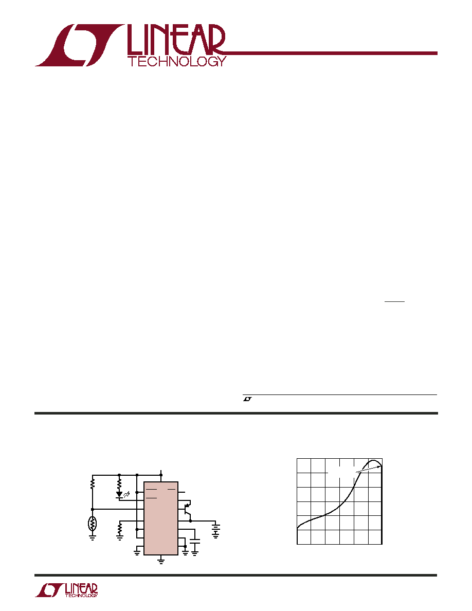
2-Cell, 2A Standalone NiMH Fast Charger with
Optional Thermistor and Charge Indicator
DESCRIPTIO
U
FEATURES
APPLICATIO S
U
TYPICAL APPLICATIO
U
The LTC
Æ
4060 is a complete fast charging system for NiMH
or NiCd batteries. Just a few external components are
needed to design a standalone linear charging system.
An external PNP transistor provides charge current that is
user programmable with a resistor. A small external capaci-
tor sets the maximum charge time. No external current
sense resistor is needed, and no blocking diode is required.
The IC automatically senses the DC input supply and bat-
tery insertion or removal. Heavily discharged batteries are
initially charged at a C/5 rate before a fast charge is applied.
Fast charge is terminated using the ≠V detection method.
Backup termination consists of a programmable timer and
battery overvoltage detector. An optional external NTC ther-
mistor can be used for temperature-based qualification of
charging. An optional programmable recharge feature au-
tomatically recharges batteries after discharge.
Manual shutdown is accomplished with the SHDN pin, while
removing input power automatically puts the LTC4060 into
sleep mode. During shutdown or sleep mode, battery drain
is <1µA.
The LTC4060 is available in both low profile (0.75mm) 16-
pin 5mm ◊ 3mm DFN and 16-lead TSSOP packages. Both
feature exposed metal die mount pads for optimum ther-
mal performance.
2-Cell NiMH Charging Profile
V
CC
V
IN
=
5V
LTC4060
GND
SHDN
CHRG
NTC
PROG
ARCT
SEL0
SEL1
ACP
SENSE
DRIVE
BAT
TIMER
CHEM
PAUSE
330
698
NTC
1.5nF
4060 TA01
NiMH
BATTERY
"CHARGE"
+
CHARGE TIME (MINUTES)
0
3.10
BATTERY VOLTAGE (V)
3.20
3.30
3.40
10
20
30
40
4060 TA01b
50
60
≠V
TERMINATION
2
LTC4060
4060f
ORDER PART
NUMBER
(Note 1)
V
CC
to GND ............................................... ≠0.3V to 11V
Input Voltage
SHDN, NTC, SEL0, SEL1, PROG, ARCT,
BAT, CHEM, TIMER, PAUSE ...... ≠0.3V to V
CC
+ 0.3V
Output Voltage
CHRG, ACP, DRIVE ................... ≠0.3V to V
CC
+ 0.3V
Output Current (SENSE) ...................................... ≠2.2A
Short-Circuit Duration (DRIVE) ...................... Indefinite
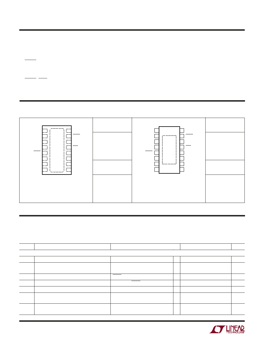
LTC4060EDHC
ABSOLUTE
M
AXI
M
U
M
RATINGS
W
W
W
U
PACKAGE/ORDER I
N
FOR
M
ATIO
N
W
U
U
Consult LTC Marketing for parts specified with wider operating temperature ranges.
Operating Ambient Temperature Range
(Note 2) ............................................. ≠ 40∞C to 85∞C
Operating Junction Temperature (Note 3) ........... 125∞C
Storage Temperature Range
TSSOP Package ............................... ≠ 65∞C to 150∞C
DFN Package .................................... ≠65∞C to 125∞C
Lead Temperature (Soldering, 10 sec)
TSSOP Package ................................................ 300∞C
16
15
14
13
12
11
10
9
17
1
2
3
4
5
6
7
8
GND
CHRG
V
CC
ACP
CHEM
NTC
SEL1
SEL0
DRIVE
BAT
SENSE
TIMER
SHDN
PAUSE
PROG
ARCT
TOP VIEW
DHC16 PACKAGE
16-LEAD (5mm ◊ 3mm) PLASTIC DFN
T
JMAX
= 125∞C,
JA
= 37∞C/W
EXPOSED PAD (PIN 17) IS GND
MUST BE SOLDERED TO PCB TO OBTAIN
JA
= 37∞C/W OTHERWISE
JA
= 140∞C
DHC PART
MARKING
4060
ORDER PART
NUMBER
LTC4060EFE
FE PART
MARKING
4060EFE
FE PACKAGE
16-LEAD PLASTIC TSSOP
1
2
3
4
5
6
7
8
TOP VIEW
16
15
14
13
12
11
10
9
DRIVE
BAT
SENSE
TIMER
SHDN
PAUSE
PROG
ARCT
GND
CHRG
V
CC
ACP
CHEM
NTC
SEL1
SEL0
17
T
JMAX
= 125∞C,
JA
= 37∞C/W
EXPOSED PAD (PIN 17) IS GND
MUST BE SOLDERED TO PCB TO OBTAIN
JA
= 37∞C/W OTHERWISE
JA
= 135∞C
The
indicates specifications which apply over the full operating
temperature range, otherwise specifications are at T
A
= 25∞C. V
CC
= 5V, V
BAT
= 2.8V, GND = 0V unless otherwise specified. All
currents into the device pins are positive and all currents out of the device pins are negative. All voltages are referenced to GND
unless otherwise specified.
ELECTRICAL CHARACTERISTICS
SYMBOL
PARAMETER
CONDITIONS
MIN
TYP
MAX
UNITS
V
CC
Supply
V
CC
Operating Voltage Range (Note 4)
4.50
10
V
I
CC
V
CC
Supply Current (Note 9)
I
PROG
= 2mA (R
PROG
= 698),
2.9
4.3
mA
PAUSE = V
CC
I
SD
V
CC
Supply Shutdown Current
SHDN = 0V
250
325
µA
I
BSD
Battery Pin Leakage Current in Shutdown (Note 5)
V
BAT
= 2.8V, SHDN = 0V
≠1
0
1
µA
I
BSL
Battery Pin Leakage Current in Sleep (Note 6)
V
CC
= 0V, V
BAT
= 5.6V
≠1
0
1
µA
V
UVI1
Undervoltage Lockout Exit Threshold
SEL0 = 0, SEL1 = 0 and SEL0 = V
CC
,
4.25
4.36
4.47
V
SEL1 = 0, V
CC
Increasing
V
UVD1
Undervoltage Lockout Entry Threshold
SEL0 = 0, SEL1 = 0 and SEL0 = V
CC
,
4.15
4.26
4.37
V
SEL1 = 0, V
CC
Decreasing
3
LTC4060
4060f
SYMBOL
PARAMETER
CONDITIONS
MIN
TYP
MAX
UNITS
The
indicates specifications which apply over the full operating
temperature range, otherwise specifications are at T
A
= 25∞C. V
CC
= 5V, V
BAT
= 2.8V, GND = 0V unless otherwise specified. All
currents into the device pins are positive and all currents out of the device pins are negative. All voltages are referenced to GND
unless otherwise specified.
ELECTRICAL CHARACTERISTICS
V
UVI2
Undervoltage Lockout Exit Threshold
SEL0 = 0, SEL1 = V
CC
, V
CC
Increasing
6.67
6.81
6.95
V
V
UVD2
Undervoltage Lockout Entry Threshold
SEL0 = 0, SEL1 = V
CC
, V
CC
Decreasing
6.57
6.71
6.85
V
V
UVI3
Undervoltage Lockout Exit Threshold
SEL0 = V
CC
, SEL1 = V
CC
, V
CC
Increasing
8.28
8.47
8.65
V
V
UVD3
Undervoltage Lockout Entry Threshold
SEL0 = V
CC
, SEL1 = V
CC
, V
CC
Decreasing
8.18
8.37
8.55
V
V
UVH
Undervoltage Lockout Hysteresis
For All SEL0, SEL1 Options
100
mV
Charging Performance
I
FCH
High Fast Charge Current (Notes 7, 10)
R
PROG
= 698, 5V < V
CC
< 10V
1.9
2
2.1
A
I
FCL
Low Fast Charge Current (Note 7)
R
PROG
= 3480, 4.5V < V
CC
< 10V
0.35
0.4
0.45
A
I
PCH
High Precharge Current (Note 7)
R
PROG
= 698, 4.5V < V
CC
< 10V
320
400
480
mA
I
PCL
Low Precharge Current (Note 7)
R
PROG
= 3480, 4.5V < V
CC
< 10V
40
80
120
mA
I
BRD
Battery Removal Detection Bias Current
4.5V < V
CC
< 10V, V
BAT
= V
CC
≠ 0.4V
≠450
≠300
≠160
µA
V
BR
Battery Removal Threshold Voltage (Note 8)
V
CELL
Increasing, 4.5V < V
CC
< 10V
1.95
2.05
2.15
V
V
BRH
Battery Removal Threshold Hysteresis Voltage
V
CELL
Decreasing
50
mV
(Note 8)
V
BOV
Battery Overvoltage Threshold (Note 8)
V
CELL
Increasing, 4.5V < V
CC
< 10V
1.85
1.95
2.05
V
V
BOVH
Battery Overvoltage Threshold Hysteresis (Note 8) V
CELL
Decreasing
50
mV
V
FCQ
Fast Charge Qualification Threshold Voltage
V
CELL
Increasing, 4.5V < V
CC
< 10V
840
900
960
mV
(Note 8)
V
FCQH
Fast Charge Qualification Threshold Hysteresis
V
CELL
Decreasing
50
mV
Voltage (Note 8)
V
IDT
Initial Delay Hold-Off Threshold Voltage (Note 8)
V
CELL
Increasing, 4.5V < V
CC
< 10V
1.24
1.3
1.36
V
V
IDTH
Initial Delay Hold-Off Threshold Hysteresis Voltage V
CELL
Decreasing
50
mV
(Note 8)
V
MDV
≠V Termination (Note 8)
CHEM = V
CC
(NiCd)
11
16
21
mV
CHEM = 0V (NiMH)
5
8
14
mV
V
PROG
Program Pin Voltage
4.5V < V
CC
< 10V, R
PROG
= 635
1.45
1.5
1.54
V
and 3480
V
ART
Automatic Recharge Programmed Threshold
V
CELL
Decreasing, V
ARCT
= 1.1V,
1.065
1.1
1.135
V
Voltage Accuracy (Note 8)
4.5V < V
CC
< 10V
V
ARDT
Automatic Recharge Default Threshold Voltage
V
CELL
Decreasing, V
ARCT
= V
CC
,
1.235
1.3
1.365
V
Accuracy (Note 8)
4.5V < V
CC
< 10V
V
ARH
Automatic Recharge Threshold Voltage Hysteresis
V
CELL
Increasing
50
mV
(Note 8)
V
ARDEF
Automatic Recharge Pin Default Enable Threshold
V
CC
V
CC
V
Voltage
≠ 0.8
≠ 0.2
V
ARDIS
Automatic Recharge Pin Disable Threshold
250
650
mV
Voltage
I
ARL
Automatic Recharge Pin Pull-Down Current
V
ARCT
= 1.3V
0.15
1.5
µA
V
CLD
NTC Pin Cold Threshold Voltage
V
NTC
Decreasing, 4.5V < V
CC
< 10V
0.83 ∑
0.86 ∑
0.89 ∑
V
V
CC
V
CC
V
CC
V
CLDH
NTC Pin Cold Threshold Hysteresis Voltage
V
NTC
Increasing
150
mV
V
HTI
NTC Pin Hot Charge Initiation Threshold Voltage
V
NTC
Decreasing, 4.5V < V
CC
< 10V
0.47 ∑
0.5 ∑
0.53 ∑
V
V
CC
V
CC
V
CC
4
LTC4060
4060f
SYMBOL
PARAMETER
CONDITIONS
MIN
TYP
MAX
UNITS
The
indicates specifications which apply over the full operating
temperature range, otherwise specifications are at T
A
= 25∞C. V
CC
= 5V, V
BAT
= 2.8V, GND = 0V unless otherwise specified. All
currents into the device pins are positive and all currents out of the device pins are negative. All voltages are referenced to GND
unless otherwise specified.
ELECTRICAL CHARACTERISTICS
V
HTIH
NTC Pin Hot Charge Initiation Hysteresis Voltage
V
NTC
Increasing
100
mV
V
HTC
NTC Pin Hot Charge Cutoff Threshold Voltage
V
NTC
Decreasing, 4.5V V
CC
10V
0.37 ∑
0.4 ∑
0.43 ∑
V
V
CC
V
CC
V
CC
V
HTCH
NTC Pin Hot Charge Cutoff Hysteresis Voltage
V
NTC
Increasing
100
mV
V
NDIS
NTC Pin Disable Threshold Voltage
25
250
mV
I
NL
NTC Pin Pull-Down Current
V
NTC
= 2.5V
0.15
1.5
µA
t
ACC
Timer Accuracy
R
PROG
= 698, C
TIMER
= 1.2nF and
≠15
0
15
%
R
PROG
= 3480, C
TIMER
= 470pF
Output Drivers
I
DRV
Drive Pin Sink Current
V
DRIVE
= 4V
40
70
120
mA
R
DRV
Drive Pin Resistance to V
CC
V
DRIVE
= 4V, Not Charging
4700
V
OL
ACP, CHRG Output Pins Low Voltage
I
ACP
= I
CHRG
= 10mA
0.8
V
I
OH
ACP, CHRG Output Pins High Leakage Current
Outputs Inactive, V
CHRG
= V
ACP
= V
CC
≠2
2
µA
Control Inputs
V
IT
SHDN, SEL0, SEL1, CHEM, PAUSE Pins Digital
V
CC
= 10V
350
650
mV
Input Threshold Voltage
V
ITH
SHDN, SEL0, SEL1, CHEM, PAUSE Pins Digital
50
mV
Input Hysteresis Voltage
I
IPD
SHDN, SEL0, SEL1, CHEM Pins Digital Input
V
CC
= 10V, V
IN
= V
CC
0.4
2
µA
Pull-Down Current
I
IPU
PAUSE Pin Digital Input Pull-Up Current
V
IN
= GND
≠2
≠0.4
µA
Note 1: Absolute Maximum Ratings only indicate limits for survivability.
Operating the device beyond these limits may result in permanent damage.
Continuous or extended application of these maximum levels may
adversely affect device reliability.
Note 2: The LTC4060 is guaranteed to meet performance specifications
from 0∞C to 70∞C ambient temperature range and 0∞C to 85∞C junction
temperature range. Specifications over the ≠40∞C to 85∞C operating
ambient temperature range are assured by design, characterization and
correlation with statistical process controls.
Note 3: This IC includes overtemperature protection that is intended to
protect the device during momentary overload conditions. Overtempera-
ture protection is activated at a temperature of approximately 145∞C,
which is above the specified maximum operating junction temperature.
Continuous operation above the specified maximum operation temperature
may result in device degradation or failure. Operating junction temperature
T
J
(in ∞C) is calculated from the ambient temperature T
A
and the average
power dissipation P
D
(in watts) by the formula:
T
J
= T
A
+
JA
∑ P
D
Note 4: Short duration drops below the minimum V
CC
specification of
several microseconds or less are ignored by the undervoltage detection
circuit.
Note 5: Assumes that the external PNP pass transistor has negligible B-C
reverse leakage current when the collector is biased at 2.8V (V
BAT
for two
charged cells in series) and the base is biased at V
CC
.
Note 6: Assumes that the external PNP pass transistor has negligible B-E
reverse leakage current when the emitter is biased at 0V (V
CC
) and the
base is biased at 5.6V (V
BAT
for four charged cells in series).
Note 7: The charge current specified is the regulated current through the
internal current sense resistor that flows into the external PNP pass
transistor's emitter. Actual battery charging current is slightly less and
depends upon PNP alpha.
Note 8: Given as a per cell voltage (V
BAT
/Number of Cells).
Note 9: Supply current includes the current programming resistor current
of 2mA. The charger is paused and not charging the battery.
Note 10: The minimum V
CC
supply is set at 5V during this test to
compensate for voltage drops due to test socket contact resistance and 2A
of current. This ensures that the supply voltage delivered to the device
under test does not fall below the UVLO entry threshold. Specification at
the minimum V
CC
of 4.5V is assured by design and characterization.
5
LTC4060
4060f
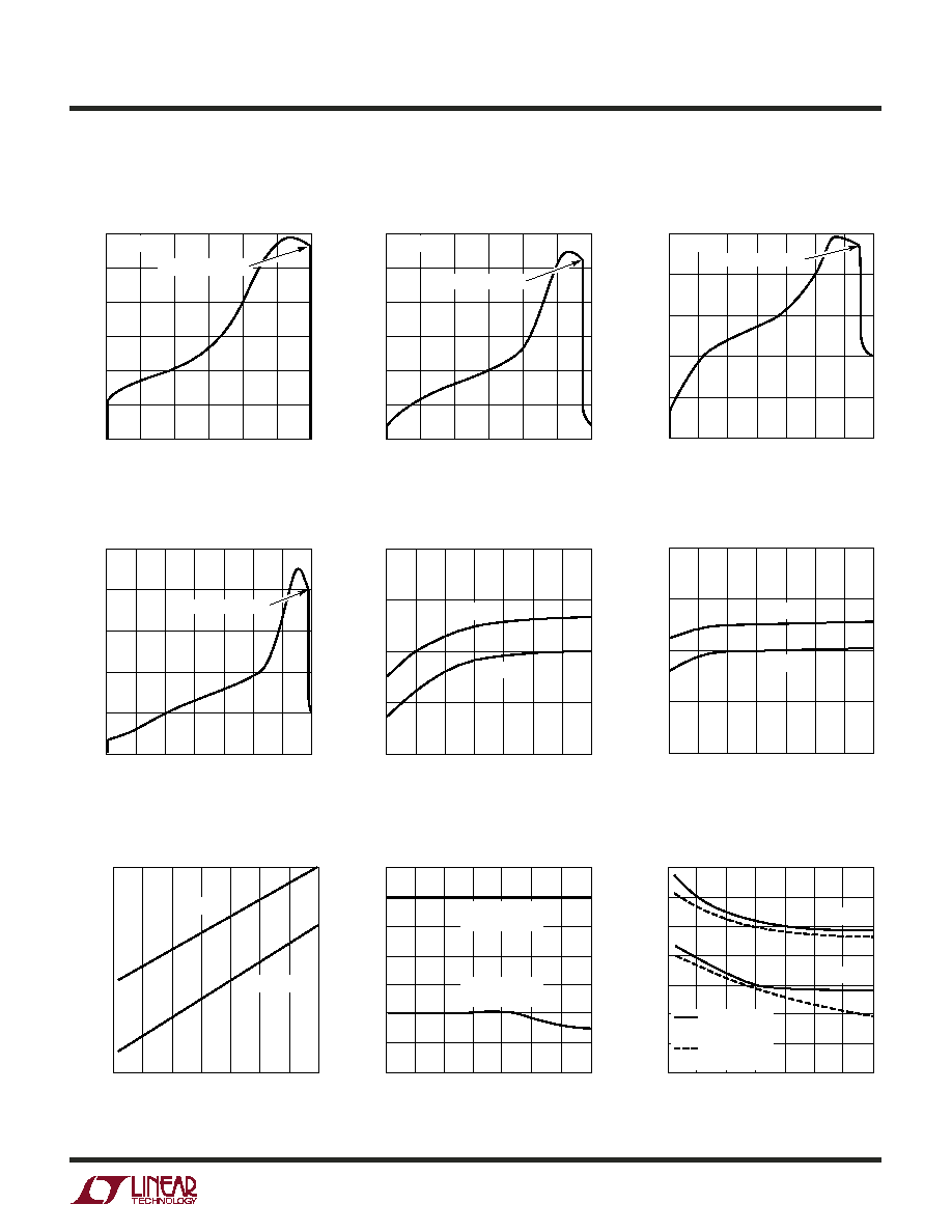
TYPICAL PERFOR A CE CHARACTERISTICS
U
W
NiMH Battery Charging
Characteristics at 1C Rate
NiCd Battery Charging
Characteristics at 1C Rate
NiMH Battery Charging
Characteristics at C/2 Rate
NiCd Battery Charging
Characteristics at C/2 Rate
I
FCH
vs Temperature and
Supply Voltage
I
FCL
vs Temperature and
Supply Voltage
I
BRD
vs Temperature and
Supply Voltage
V
MDV
vs Temperature and
Supply Voltage
t
ACC
vs Temperature and
Supply Voltage
CHARGE TIME (MINUTES)
0
1.4
CELL VOLTAGE (V) 1.5
1.6
1.7
10
20
30
40
4060 G02
50
60
≠V TERMINATION
T
A
= 25∞C
CHARGE TIME (MINUTES)
0
20
1.35
CELL VOTLAGE (V)
1.45
1.60
40
80
100
4060 G03
1.40
1.55
1.50
60
120
140
≠V TERMINATION
T
A
= 25∞C
CHARGE TIME (MINUTES)
0
20
1.40
CELL VOTLAGE (V)
1.50
1.65
40
80
100
4060 G04
1.45
1.60
1.55
60
120
140
≠V TERMINATION
TEMPERATURE (∞C)
≠50
1.990
I
FCH
(A)
1.995
2.000
2.005
2.010
≠25
0
25
50
4060 G05
75
100
125
V
CC
= 10V
V
CC
= 4.5V
TEMPERATURE (∞C)
≠50
398
I
FCL
(mA)
399
400
401
402
≠25
0
25
50
4060 G06
75
100
125
V
CC
= 10V
V
CC
= 4.5V
TEMPERATURE (∞C)
≠50
≠340
I
BRD
(
µ
A)
≠300
≠260
≠25
0
25
50
4060 G07
75
100
125
V
CC
= 10V
V
CC
= 4.5V
TEMPERATURE (∞C)
≠50
12
14
18
25
75
4060 G08
10
8
≠25
0
50
100
125
6
4
16
V
MDV
(mV)
NiCd
4.5V V
CC
10V
NiMH
4.5V V
CC
10V
TEMPERATURE (∞C)
≠50
0.5
1.0
1.7
25
75
4060 G09
0
≠0.5
≠25
0
50
100
125
≠1.0
≠1.5
1.5
ERROR (%)
V
CC
= 10V
V
CC
= 4.5V
R
PROG
= 3480
C
TIMER
= 470pF
R
PROG
= 698
C
TIMER
= 1.2nF
CHARGE TIME (MINUTES)
0
1.55
CELL VOLTAGE (V) 1.60
1.65
1.70
10
20
30
40
4060 G01
50
60
≠V TERMINATION
T
A
= 25∞C