 | –≠–ª–µ–∫—Ç—Ä–æ–Ω–Ω—ã–π –∫–æ–º–ø–æ–Ω–µ–Ω—Ç: LM119 | –°–∫–∞—á–∞—Ç—å:  PDF PDF  ZIP ZIP |

1
LT119A/LT319A
LM119/LM319
s
Guaranteed Maximum 0.5mV Input Offset Voltage
s
Input Protection Diodes
s
Operates From Single 5V Supply
s
25mA Drive Capability
s
80ns Response Time
The LT119A is an improved version of the LM119 dual
comparator. It features lower input offset voltage and
offset current, higher voltage gain, guaranteed common
mode rejection, and input protection diodes.
The LT119A is capable of operation over a supply range
from 5V to
±
15V and can drive 25mA loads from each open
collector output. A separate ground pin allows the LT119A
to isolate system grounds.
Linear Technology Corporation's advanced processing,
design techniques and reliability make the LT119A/LT319A
an ideal choice over previous devices in most comparator
applications.
Dual Comparator
FEATURES
DESCRIPTIO
N
U
s
Window Detectors
s
High Speed One Shot
s
Relay/Lamp Drivers
s
Voltage Controlled Oscillators
APPLICATIO
N
S
U
TYPICAL APPLICATIO
N
U
≠
+
≠
+
5V
500
TTL OUTPUT
LT119/319 TA1
1
10
3
4
8
9
5
7
6
2
1
/
2
LT319A
1
/
2
LT319A
V
UT
V
OUT
= 5.0V FOR
V
LT
V
IN
V
UT
V
OUT
= 0V FOR
V
IN
V
LT
OR V
IN
V
UT
V
IN
V
LT
*
ALLOWED WINDOW FOR SINGLE
+
5V SUPPLY IS 1.2V TO 3.8V
Window Detector*
TIME (ns)
0
INPUT
VOLTAGE (mV)
OUTPUT
VOLTAGE (V)
50
0
1
2
4
50
150
200
LT119/319 TA2
100
5
6
3
0
100
250 300
350
20mV
2mV
5mV
V
S
= ±15V
R
L
= 500
V
++
= 5V
T
A
= 25∞C
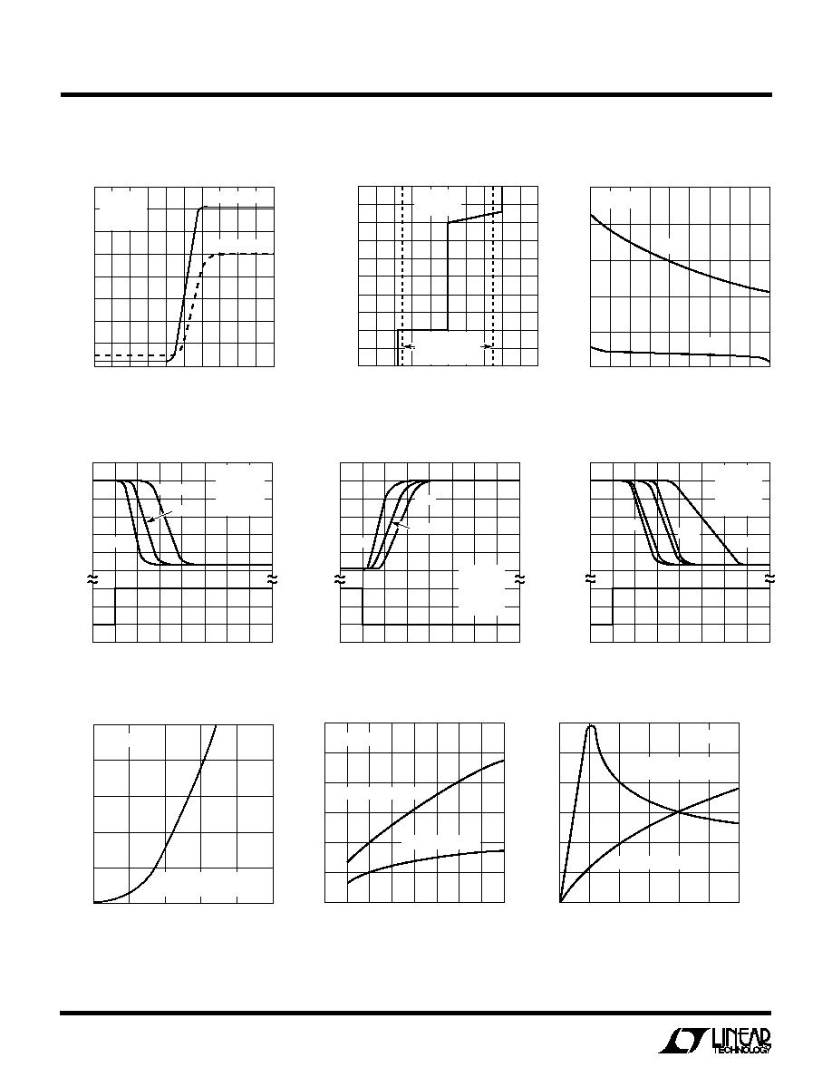
Response Time for Various Input Overdrives
2
LT119A/LT319A
LM119/LM319
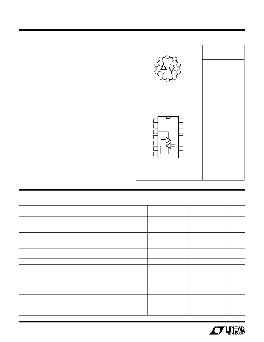
PACKAGE/ORDER I
N
FOR
M
ATIO
N
W
U
U
ABSOLUTE
M
AXI
M
U
M
RATINGS
W
W
W
U
T
JMAX
= 150
∞
C,
JA
= 150
∞
C/ W,
Jc
= 45
∞
C/ W
1
2
3
4
5
6
7
TOP VIEW
J PACKAGE
14-LEAD CERAMIC DIP
N PACKAGE
14-LEAD PLASTIC DIP
14
13
12
11
10
9
8
NC
NC
GND
+INPUT
≠ INPUT
V
≠
OUTPUT 2
NC
NC
OUTPUT 1
V
+
≠ INPUT 2
+INPUT 2
GND 2
T
JMAX
= 150
∞
C,
JA
= 100
∞
C/ W (J)
T
JMAX
= 85
∞
C,
JA
= 100
∞
C/ W (N)
ELECTRICAL CHARACTERISTICS
Supply Voltage ........................................................ 36V
Output to Negative Supply Voltage .......................... 36V
Ground to Negative Supply Voltage ......................... 25V
Ground to Positive Supply Voltage .......................... 18V
Differential Input Voltage (Note 5) ..........................
±
5V
Differential Input Current (Note 5) ........................
±
5mA
Input Voltage (Note 1)
Output Short-Circuit Duration ................................... 10s
Operating Temperature Range
LT119A, LM119 ............................... ≠ 55
∞
C to 125
∞
C
LT319A, LM319 ...................................... 0
∞
C to 70
∞
C
Storage Temperature Range ................. ≠ 65
∞
C to 150
∞
C
Lead Temperature (Soldering, 10 sec).................. 300
∞
C
Consult factory for Industrial and Military grade parts.
LT119A
LT119
SYMBOL
PARAMETER
CONDITIONS
MIN
TYP
MAX
MIN
TYP
MAX
UNITS
V
OS
Input Offset Voltage
V
S
=
±
15V, V
CM
= 0
0.3
0.5
4
mV
V
OS
Input Offset Voltage
(Note 3)
0.5
1.0
0.7
4
mV
q
1.2
2.0
7
mV
CMRR
Common-Mode Rejection Ratio
90
106
dB
I
OS
Input Offset Current
(Note 3)
20
40
30
75
nA
q
75
100
nA
I
B
Input Bias Current
(Note 3)
150
500
150
500
nA
q
1000
1000
nA
A
V
Voltage Gain
20
40
10
40
V/mV
Response Time
(Note 4)
80
80
ns
V
SAT
Saturation Voltage
V
IN
≠5mV, I
O
= 25mA
0.75
1.5
0.75
1.5
V
V
+
4.5V, V
≠
= 0V
V
IN
≠6mA, I
SINK
3.2mA
T
A
0
∞
C
0.23
0.4
0.23
0.4
V
T
A
0
∞
C
0.6
0.6
V
Output Leakage Current
V
IN
5mV, V
OUT
= 35V
0.2
2
0.2
2
µ
A
q
1
10
1
10
µ
A
Input Voltage Range
V
S
=
±
15V
q
≠12
±
13
12
≠12
±
13
12
V
V
+
= 5V, V
≠
= 0V
q
1
3
1
3
V
(Note 2)
TOP VIEW
≠ INPUT 2
V
+
V
≠
10
9
8
6
4
2
1
5
H PACKAGE
10-LEAD TO-5 METAL CAN
7
3
GND 2
OUTPUT 2
+INPUT 1
≠INPUT 1
GND
OUTPUT 1
+INPUT 2
LT119AH
LM119H
LT319AH
LM319H
LT119AJ
LM119J
LT319AJ
LM319J
LT319AN
LM319N
ORDER PART
NUMBER
3
LT119A/LT319A
LM119/LM319
ELECTRICAL CHARACTERISTICS
(Note 2)
LT119A
LT119
SYMBOL
PARAMETER
CONDITIONS
MIN
TYP
MAX
MIN
TYP
MAX
UNITS
Differential Input Voltage
q
±
5
±
5
V
I
S
Supply Current
V
+
= 5V, V
≠
= 0V
4.3
4.3
mA
I
S
Positive Supply Current
V
S
=
±
15V
8
11.5
8
11.5
mA
I
S
Negative Supply Current
V
S
=
±
15V
3
4.5
3
4.5
mA
V
OS
Input Offset Voltage
V
S
=
±
15V, V
CM
= 0V
0.3
0.5
8
mV
V
OS
Input Offset Voltage
R
S
5k
0.5
1
2
8
mV
(Note 3)
q
2
10
mV
CMRR
Common-Mode Rejection Ratio
90
106
dB
I
OS
Input Offset Current
(Note 3)
30
40
80
200
nA
q
60
300
nA
I
B
Input Bias Current
(Note 3)
150
500
250
1000
nA
q
1000
1200
nA
A
V
Voltage Gain
20
40
8
40
V/mV
Response Time
(Note 4)
80
80
ns
V
SAT
Saturation Voltage
V
IN
≠10mV, I
SINK
= 25mA
T
A
= 25
∞
C
0.75
1.5
0.75
1.5
V
V
+
4.5V, V
≠
= 0V
V
IN
≠10mV, I
SINK
3.2mA
q
0.3
0.4
0.3
0.4
V
Output Leakage Current
V
IN
10mV, V
OUT
= 35V
0.2
10
0.2
10
µ
A
Input Voltage Range
V
S
=
±
15V
q
±
13
±
13
V
V
+
= 5V, V
≠
= 0V
q
1
3
1
3
V
Differential Input Voltage
q
±
5
±
5
V
I
S
Supply Current
V
+
= 5V, V
≠
= 0V
4.3
4.3
mA
I
S
Positive Supply Current
V
S
=
±
15V
8
12.5
8
12.5
mA
I
S
Negative Supply Current
V
S
=
±
15V
3
5
3
5
mA
The
q
denotes specifications which apply over the full operating
temperature range.
Note 1: For supply voltages less than
±
15V, the maximum input voltage is
equal to the supply voltage.
Note 2: Unless otherwise noted, supply voltage equals
±
15V and
T
A
= 25
∞
C. The ground pin is grounded. Note that the maximum voltage
allowed between the ground pin and V
+
is 18V. Do not tie the ground pin
to V
≠
when the power supply voltage exceeds
±
9V. The offset voltage,
offset current and bias current specifications apply for all supply voltages
between
±
15V and 5V unless otherwise specified.
Note 3: The offset voltages and currents given are the maximum values
required to drive the output within 1V of either supply with a 1mA load,
thus these parameters define an error band and take into account the
worst case effects of voltage gain and input impedance.
Note 4: Response time specified is for a 100mV input step with 5mV
overdrive.
Note 5: Inputs are protected with back-to-back 5.6V zener diodes. This
limits maximum differential input voltage to
±
5V if current is unlimited.
Larger differential input drive is allowed if input current is limited to
±
5mA
with external resistance.
4
LT119A/LT319A
LM119/LM319
TYPICAL PERFOR
M
A
N
CE CHARACTERISTICS
U
W
Input Currents
Transfer Function
Response Time for Various
Input Overdrives
TIME (ns)
≠100
INPUT
VOLTAGE (mV)
OUTPUT
VOLTAGE (V)
≠50
0
1
2
4
50
150
200
LT119/319 G4
0
5
6
3
0
100
250 300
350
2mV
20mV
5mV
V
S
= ±15V
R
L
= 500
V
++
= 5V
T
A
= 25∞C
Response Time for Various
Input Overdrives
TIME (ns)
≠100
INPUT
VOLTAGE (mV)
OUTPUT
VOLTAGE (V)
≠50
0
1
2
4
50
150
200
LT119/319 G6
0
5
6
3
0
100
250 300
350
20mV
2mV
5mV
V
S
= 5V
R
L
= 500
V
++
= 5V
T
A
= 25∞C
Output Saturation Voltage
OUTPUT VOLTAGE (V)
0
OUTPUT CURRENT (mA)
15
20
25
0.8
LT119/319 G7
10
5
0
0.2
0.4
0.6
1.0
V
S
= ±15V
INPUT OVERDRIVE = 5mV
T
J
= 25∞C
OUTPUT VOLTAGE (V)
0
0
SHORT-CIRCUIT CURRENT (mA)
20
40
60
80
120
5
10
LT119/319 G9
15
100
0
POWER DISSIPATION (W)
0.2
0.4
0.6
0.8
1.2
1.0
T
J
= 25∞C
SHORT-CIRCUIT CURRENT
AFTER 3 MINUTES
POWER DISSIPATION
Supply Current
Response Time for Various
Input Overdrives
TIME (ns)
0
INPUT
VOLTAGE (mV)
OUTPUT
VOLTAGE (V)
50
0
1
2
4
50
150
200
LT119/319 G5
100
5
6
3
0
100
250 300
350
20mV
2mV
5mV
V
S
= 5V
R
L
= 500
V
++
= 5V
T
A
= 25∞C
DIFFERENTIAL INPUT VOLTAGE (V)
≠10
INPUT BIAS CURRENT (nA)
200
300
400
6
LT119/319 G2
100
0
≠100
≠6
≠2
2
10
V
S
= ±15V
T
A
= 25∞C
MAXIMUM
DIFFERENTIAL
INPUT VOLTAGE
Input Characteristics
SUPPLY VOLTAGE (V)
0
0
SUPPLY CURRENT (mA)
2
4
6
8
5
10
15
20
LT119/319 G8
10
12
POSITIVE SUPPLY
NEGATIVE SUPPLY
T
J
= 25∞C
DIFFERENTIAL INPUT VOLTAGE (mV)
≠1.0
OUTPUT VOLTAGE HIGH (V)
OUTPUT VOLTAGE LOW (V)
30
40
0.6
LT119/319 G1
20
10
0
≠0.6
≠0.2
0.2
1.0
25
35
15
5.0
6
8
4
2
0
5
7
3
1
V
++
= 36V
V
++
= 5V
V
S
= ±15V
R
L
= 1.4k
T
A
= 25∞C
TEMPERATURE (∞C)
≠ 55
0
INPUT CURRENT (nA)
50
150
200
250
≠15
25
45
125
LT119/319 G3
100
≠35
5
65
85 105
V
S
= ±15V
BIAS
OFFSET
Output Limiting Characteristics

5
LT119A/LT319A
LM119/LM319
10
5V
1
2
3
4
LT119/319 TA5
1
/
2
LT319A
OUTPUT
39k
1k
20k
20k
2k
≠
+
≠
+
1k
100k
10k
INPUT
0V TO 5V
AT CUT
18pF, 100kHz
1000pF
MV1405*
5V
3k
5V
5
7
6
8
9
1
/
2
LT319A
1
/
2
LT319A
TYPICAL PERFOR
M
A
N
CE CHARACTERISTICS
U
W
Common-Mode Limits
Supply Current
TYPICAL APPLICATIO
N
S
U
Relay Driver
High Noise Immunity 60Hz Sync Circuit
10
6
5V
7
5
8
9
≠
+
LT119/319 TA4
1
/
2
LT319A
OUTPUT
3.3k
10k
20k
0.15µF
10k
68k
1N4148
60Hz
INPUT
10V
P≠P
(TYP)
10
6
28V
5V
7
5
8
9
≠
+
35V
LT119/319 TA3
INPUTS
1
/
2
LT319A
Voltage Controlled Crystal Oscillator
With 100PPM Trim Range
0
SUPPLY CURRENT (mA)
2
6
8
10
LT119/319 G11
4
12
TEMPERATURE (∞C)
≠ 55 ≠ 35 ≠15
85 105 125
25
5
45
65
POSITIVE SUPPLY = 15V
POSITIVE SUPPLY = 5V, V
≠
= 0V
NEGATIVE SUPPLY = ≠15V
TEMPERATURE (∞C)
≠ 55 ≠ 35 ≠15
V
≠
COMMON-MODE LIMITS (V)
0.4
1.2
≠2.0
≠1.6
85 105 125
V
+
LT119/319 G10
0.8
25
5
45
65
≠1.2
≠0.8
≠0.4
V
+
= 5V, V
≠
= 0V
V
S
= ±15V
V
S
= ±15V, V
+
= 5V, V
≠
= 0V
REFERRED TO SUPPLY VOLTAGES