 | –≠–ª–µ–∫—Ç—Ä–æ–Ω–Ω—ã–π –∫–æ–º–ø–æ–Ω–µ–Ω—Ç: LT1007C | –°–∫–∞—á–∞—Ç—å:  PDF PDF  ZIP ZIP |
1
LT1007/LT1037
100737fb
FEATURES
DESCRIPTIO
U
APPLICATIO S
U
TYPICAL APPLICATIO
U
Low Noise, High Speed
Precision Operational Amplifiers
s
Guaranteed 4.5nV/
Hz 10Hz Noise
s
Guaranteed 3.8nV/
Hz 1kHz Noise
s
0.1Hz to 10Hz Noise, 60nV
P-P
Typical
s
Guaranteed 7 Million Min Voltage Gain, R
L
= 2k
s
Guaranteed 3 Million Min Voltage Gain, R
L
= 600
s
Guaranteed 25
µ
V Max Offset Voltage
s
Guaranteed 0.6
µ
V/
∞
C Max Drift with Temperature
s
Guaranteed 11V/
µ
s Min Slew Rate (LT1037)
s
Guaranteed 117dB Min CMRR
The LT
Æ
1007/LT1037 series features the lowest noise
performance available to date for monolithic operational
amplifiers: 2.5nV/
Hz wideband noise (less than the noise of
a 400
resistor), 1/f corner frequency of 2Hz and 60nV peak-
to-peak 0.1Hz to 10Hz noise. Low noise is combined with
outstanding precision and speed specifications: 10
µ
V offset
voltage, 0.2
µ
V/
∞
C drift, 130dB common mode and power
supply rejection, and 60MHz gain bandwidth product on the
decompensated LT1037, which is stable for closed-loop
gains of 5 or greater.
The voltage gain of the LT1007/LT1037 is an extremely high
20 million driving a 2k
load and 12 million driving a 600
load to
±
10V.
In the design, processing and testing of the device, particular
attention has been paid to the optimization of the entire
distribution of several key parameters. Consequently, the
specifications of even the lowest cost grades (the LT1007C
and the LT1037C) have been spectacularly improved com-
pared to equivalent grades of competing amplifiers.
The sine wave generator application shown below utilizes the
low noise and low distortion characteristics of the LT1037.
, LTC and LT are registered trademarks of Linear Technology Corporation.
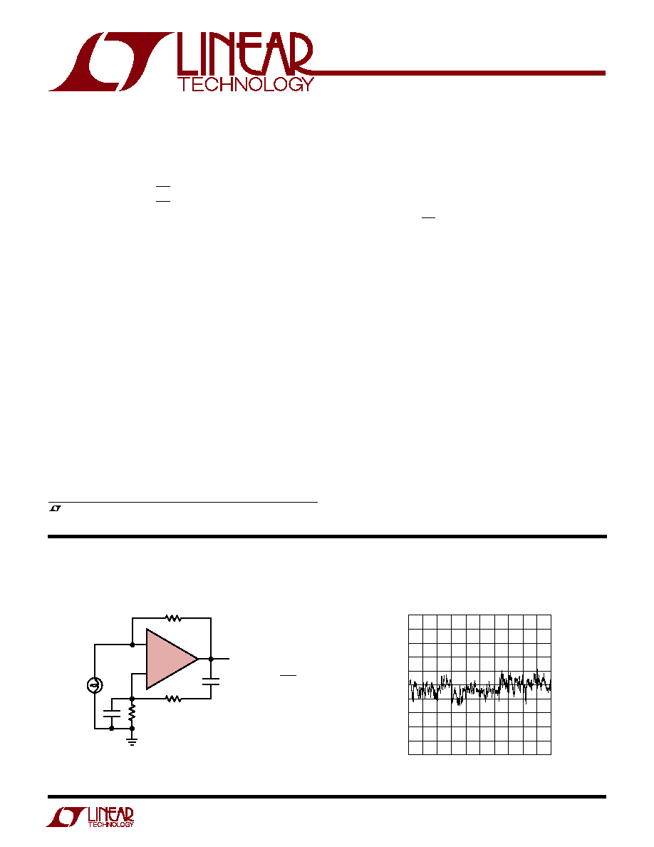
Ultrapure 1kHz Sine Wave Generator
TIME (SEC)
0
2
4
6
8
10
VOLTAGE NOISE (20nV/DIV)
1007/37 TA02
s
Low Noise Signal Processing
s
Microvolt Accuracy Threshold Detection
s
Strain Gauge Amplifiers
s
Direct Coupled Audio Gain Stages
s
Sine Wave Generators
s
Tape Head Preamplifiers
s
Microphone Preamplifiers
1007/37 TA01
430
OUTPUT
C
C
R
R
6
2
3
#327 LAMP
≠
+
LT1037
f =
1
2
RC
R = 1591.5
±
0.1%
C = 0.1
µ
F
±
0.1%
TOTAL HARMONIC DISTORTION = < 0.0025%
NOISE = < 0.0001%
AMPLITUDE =
±
8V
OUTPUT FREQUENCY = 1.000kHz FOR VALUES GIVEN
±
0.4%
0.1Hz to 10Hz Noise
2
LT1007/LT1037
100737fb
ABSOLUTE
M
AXI
M
U
M
RATINGS
W
W
W
U
PACKAGE/ORDER I
N
FOR
M
ATIO
N
W
U
U
Supply Voltage ......................................................
±
22V
Input Voltage ............................ Equal to Supply Voltage
Output Short-Circuit Duration .......................... Indefinite
Differential Input Current (Note 9) .....................
±
25mA
Storage Temperature Range ................. ≠ 65
∞
C to 150
∞
C
TOP VIEW
V
+
V
OS
TRIM
V
OS
TRIM
≠IN
OUT
NC
+IN
V
≠
(CASE)
8
7
6
5
1
4
H PACKAGE
8-LEAD TO-5 METAL CAN
≠
+
2
3
T
JMAX
= 150
∞
C,
JA
= 150
∞
C/ W,
JC
= 45
∞
C/ W
1
2
3
4
8
7
6
5
TOP VIEW
V
OS
TRIM
V
OS
TRIM
V
+
OUT
NC
≠IN
+IN
V
≠
≠
+
N8 PACKAGE
8-LEAD PDIP
TOP VIEW
S8 PACKAGE
8-LEAD PLASTIC SO
1
2
3
4
8
7
6
5
V
OS
TRIM
V
OS
TRIM
V
+
OUT
NC
≠IN
+IN
V
≠
≠
+
T
JMAX
= 150
∞
C,
JA
= 190
∞
C/ W
ORDER PART NUMBER
ORDER PART NUMBER
ORDER PART NUMBER
1007
1007I
1037
1037I
LT1007ACN8
LT1007CN8
LT1007IN8
LT1037ACN8
LT1037CN8
LT1037IN8
LT1007ACH
LT1007AMH
LT1007CH
LT1007MH
LT1037ACH
LT1037AMH
LT1037CH
LT1037MH
T
JMAX
= 100
∞
C,
JA
= 130
∞
C/ W (N8)
S8 PART MARKING
LT1007CS8
LT1007IS8
LT1037CS8
LT1037IS8
(Note 1)
Consult LTC Marketing for parts specified with wider operating temperature ranges.
Lead Temperature (Soldering, 10 sec.)................. 300
∞
C
Operating Temperature Range
LT1007/LT1037AC, C ............................. 0
∞
C to 70
∞
C
LT1007/LT1037I ............................... ≠ 40
∞
C to 85
∞
C
LT1007/LT1037AM, M (OBSOLETE) ≠ 55
∞
C to 125
∞
C
LT1007ACJ8
LT1007AMJ8
LT1007CJ8
LT1007MJ8
LT1037ACJ8
LT1037AMJ8
LT1037CJ8
LT1037MJ8
T
JMAX
= 150
∞
C,
JA
= 100
∞
C/ W (J8)
J8 PACKAGE
LEAD CERDIP
OBSOLETE PACKAGE
OBSOLETE PACKAGE
ELECTRICAL CHARACTERISTICS
V
S
=
±
15V, T
A
= 25
∞
C, unless otherwise noted.
LT1007AC/AM
LT1007C/I/M
LT1037AC/AM
LT1037C/I/M
SYMBOL
PARAMETER
CONDITIONS
MIN
TYP
MAX
MIN
TYP
MAX
UNITS
V
OS
Input Offset Voltage
(Note 2)
10
25
20
60
µ
V
V
OS
Long Term Input Offset
(Notes 3, 4)
0.2
1.0
0.2
1.0
µ
V/Mo
Time
Voltage Stability
I
OS
Input Offset Current
7
30
12
50
nA
I
B
Input Bias Current
±
10
±
35
±
15
±
55
nA
e
n
Input Noise Voltage
0.1Hz to 10Hz (Notes 4, 6)
0.06
0.13
0.06
0.13
µ
V
P-P
Input Noise Voltage Density
f
O
= 10Hz (Notes 4, 5)
2.8
4.5
2.8
4.5
nV/
Hz
f
O
= 1000Hz (Note 4)
2.5
3.8
2.5
3.8
nV/
Hz
i
n
Input Noise Current Density
f
O
= 10Hz (Notes 4, 7)
1.5
4.0
1.5
4.0
pA/
Hz
f
O
= 1000Hz (Notes 4, 7)
0.4
0.6
0.4
0.6
pA/
Hz
Consider the N8 Package for Alternate Source
Consider the N8 or S8 Package for Alternate Source
3
LT1007/LT1037
100737fb
ELECTRICAL CHARACTERISTICS
V
S
=
±
15V, T
A
= 25
∞
C, unless otherwise noted.
LT1007AC/AM
LT1007C/I/M
LT1037AC/AM
LT1037C/I/M
SYMBOL
PARAMETER
CONDITIONS
MIN
TYP
MAX
MIN
TYP
MAX
UNITS
Input Resistance, Common Mode
7
5
G
Input Voltage Range
±
11.0
±
12.5
±
11.0
±
12.5
V
CMRR
Common Mode Rejection Ratio
V
CM
=
±
11V
117
130
110
126
dB
PSRR
Power Supply Rejection Ratio
V
S
=
±
4V to
±
18V
110
130
106
126
dB
A
VOL
Large-Signal Voltage Gain
R
L
2k, V
O
=
±
12V
7.0
20.0
5.0
20.0
V/
µ
V
R
L
1k, V
O
=
±
10V
5.0
16.0
3.5
16.0
V/
µ
V
R
L
600
, V
O
=
±
10V
3.0
12.0
2.0
12.0
V/
µ
V
V
OUT
Maximum Output Voltage Swing
R
L
2k
±
13.0
±
13.8
±
12.5
±
13.5
V
R
L
600
±
11.0
±
12.5
±
10.5
±
12.5
V
SR
Slew Rate
LT1007
R
L
2k
1.7
2.5
1.7
2.5
V/
µ
s
LT1037
A
VCL
5
11
15
11
15
V/
µ
s
GBW
Gain Bandwidth
LT1007
f
O
= 100kHz (Note 8)
5.0
8.0
5.0
8.0
MHz
Product
LT1037
f
O
= 10kHz (Note 8) (A
VCL
5)
45
60
45
60
MHz
Z
O
Open-Loop Output Resistance
V
O
= 0V, I
O
= 0
70
70
P
D
Power Dissipation
LT1007
80
120
80
140
mW
LT1037
80
130
85
140
mW
LT1007AC
LT1007C
LT1037AC
LT1037C
SYMBOL
PARAMETER
CONDITIONS
MIN
TYP
MAX
MIN
TYP
MAX
UNITS
V
OS
Input Offset Voltage
(Note 2)
q
20
50
35
110
µ
V
V
OS
Average Input Offset Drift
(Note 10)
q
0.2
0.6
0.3
1.0
µ
V/
∞
C
Temp
I
OS
Input Offset Current
q
10
40
15
70
nA
I
B
Input Bias Current
q
±
14
±
45
±
20
±
75
nA
Input Voltage Range
q
±
10.5
±
11.8
±
10.5
±
11.8
V
CMRR
Common Mode Rejection Ratio
V
CM
=
±
10.5V
q
114
126
106
120
dB
PSRR
Power Supply Rejection Ratio
V
S
=
±
4.5V to
±
18V
q
106
126
102
120
dB
A
VOL
Large-Signal Voltage Gain
R
L
2k, V
O
=
±
10V
q
4.0
18.0
2.5
18.0
V/
µ
V
R
L
1k, V
O
=
±
10V
q
2.5
14.0
2.0
14.0
V/
µ
V
V
OUT
Maximum Output Voltage Swing
R
L
2k
q
±
12.5
±
13.6
±
12.0
±
13.6
V
P
D
Power Dissipation
q
90
144
90
160
mW
The
q
denotes the specifications which apply over the temperature range 0
∞
C
T
A
70
∞
C, V
S
=
±
15V, unless otherwise noted.

4
LT1007/LT1037
100737fb
The
q
denotes the specifications which apply over the temperature range ≠ 40
∞
C
T
A
85
∞
C, V
S
=
±
15V, unless otherwise noted.
ELECTRICAL CHARACTERISTICS
For MIL-STD components, please refer to LTC 883C data sheet for test
listing and parameters.
Note 1: Absolute Maximum Ratings are those values beyond which the life
of a device may be impaired.
Note 2: Input Offset Voltage measurements are performed by automatic
test equipment approximately 0.5 seconds after application of power. AM
and AC grades are guaranteed fully warmed up.
Note 3: Long Term Input Offset Voltage Stability refers to the average
trend line of Offset Voltage vs Time over extended periods after the first 30
days of operation. Excluding the initial hour of operation, changes in V
OS
during the first 30 days are typically 2.5
µ
V. Refer to typical performance
curve.
Note 4: This parameter is tested on a sample basis only.
Note 5: 10Hz noise voltage density is sample tested on every lot. Devices
100% tested at 10Hz are available on request.
Note 6: See the test circuit and frequency response curve for 0.1Hz to
10Hz tester in the Applications Information section.
Note 7: See the test circuit for current noise measurement in the
Applications Information section.
Note 8: This parameter is guaranteed by design and is not tested.
Note 9: The inputs are protected by back-to-back diodes. Current limiting
resistors are not used in order to achieve low noise. If differential input
voltage exceeds
±
0.7V, the input current should be limited to 25mA.
Note 10: The Average Input Offset Drift performance is within the
specifications unnulled or when nulled with a pot having a range of 8k
to
20k
.
The
q
denotes the specifications which apply over the temperature range ≠ 55
∞
C
T
A
125
∞
C, V
S
=
±
15V, unless otherwise noted.
LT1007I/LT1037I
SYMBOL
PARAMETER
CONDITIONS
MIN
TYP
MAX
UNITS
V
OS
Input Offset Voltage
(Note 2)
q
40
125
µ
V
V
OS
Average Input Offset Drift
(Note 10)
q
0.3
1.0
µ
V/
∞
C
Temp
I
OS
Input Offset Current
q
20
80
nA
I
B
Input Bias Current
q
±
25
±
90
nA
Input Voltage Range
q
±
10
±
11.7
V
CMRR
Common Mode Rejection Ratio
V
CM
=
±
10.5V
q
105
120
dB
PSRR
Power Supply Rejection Ratio
V
S
=
±
4.5V to
±
18V
q
101
120
dB
A
VOL
Large-Signal Voltage Gain
R
L
2k, V
O
=
±
10V
q
2.0
15.0
V/
µ
V
R
L
1k, V
O
=
±
10V
q
1.5
12.0
V/
µ
V
V
OUT
Maximum Output Voltage Swing
R
L
2k
q
±
12.0
±
13.6
V
P
D
Power Dissipation
q
95
165
mW
LT1007AM/LT1037AM LT1007M/LT1037M
SYMBOL
PARAMETER
CONDITIONS
MIN
TYP
MAX
MIN
TYP
MAX
UNITS
V
OS
Input Offset Voltage
(Note 2)
q
25
60
50
160
µ
V
V
OS
Average Input Offset Drift
(Note 10)
q
0.2
0.6
0.3
1.0
µ
V/
∞
C
Temp
I
OS
Input Offset Current
q
15
50
20
85
nA
I
B
Input Bias Current
q
±
20
±
60
±
35
±
95
nA
Input Voltage Range
q
±
10.3
±
11.5
±
10.3
±
11.5
V
CMRR
Common Mode Rejection Ratio
V
CM
=
±
10.3V
q
112
126
104
120
dB
PSRR
Power Supply Rejection Ratio
V
S
=
±
4.5V to
±
18V
q
104
126
100
120
dB
A
VOL
Large-Signal Voltage Gain
R
L
2k, V
O
=
±
10V
q
3.0
14.0
2.0
14.0
V/
µ
V
R
L
1k, V
O
=
±
10V
q
2.0
10.0
1.5
10.0
V/
µ
V
V
OUT
Maximum Output Voltage Swing
R
L
2k
q
±
12.5
±
13.5
±
12.0
±
13.5
V
P
D
Power Dissipation
q
100
150
100
170
mW

5
LT1007/LT1037
100737fb
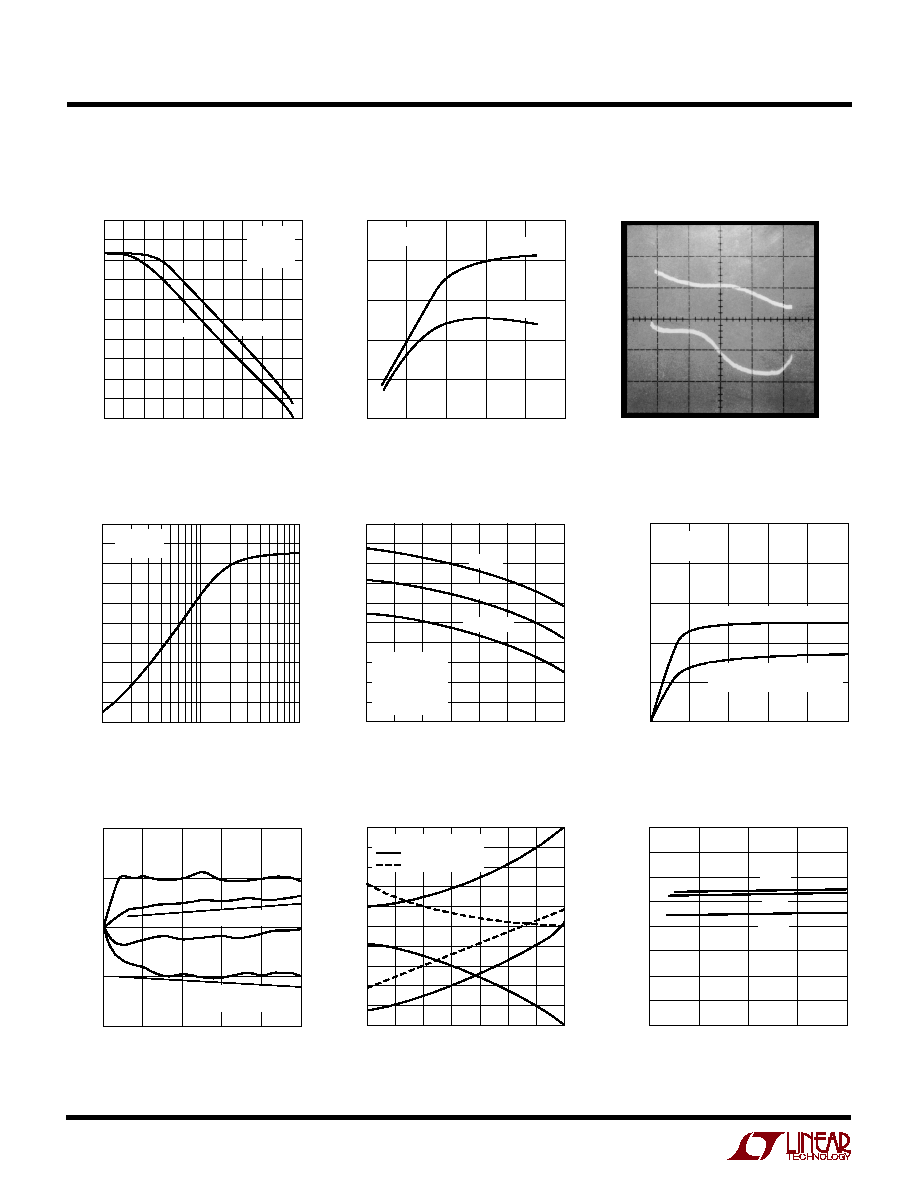
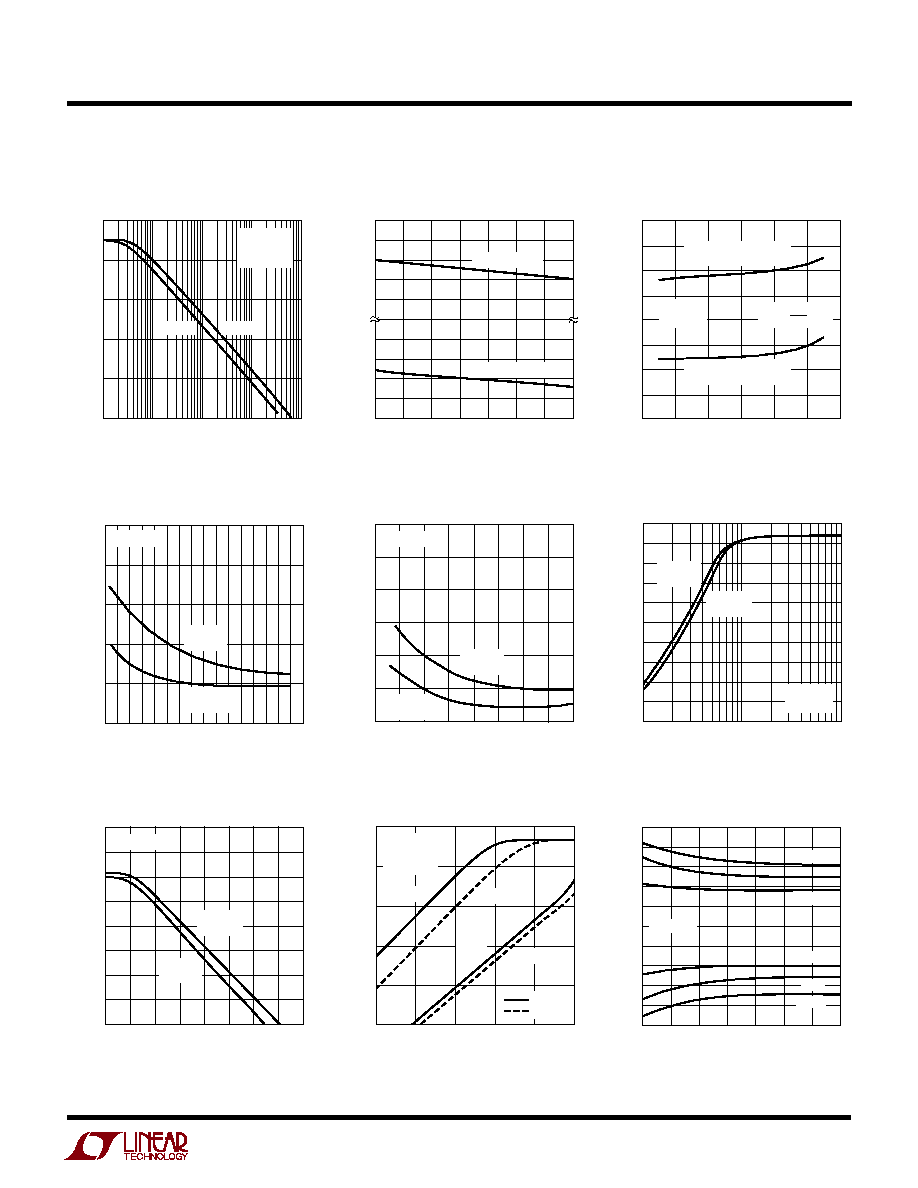
TYPICAL PERFOR
M
A
N
CE CHARACTERISTICS
U
W
VOLTAGE NOISE DENSITY (nV/
Hz)
0
NUMBER OF UNITS
140
120
100
80
60
40
20
0
1
5
7
1007/37 G01
4
9
10
2
3
6
8
V
S
=
±
15V
T
A
= 25
∞
C
497 UNITS MEASURED
FROM SIX RUNS
FREQUENCY (Hz)
1
1
3
RMS VOLTAGE NOISE DENSITY (nV/
Hz)
10
30
100
10
1000
1007/37 G02
0.1
100
V
S
=
±
15V
T
A
= 25
∞
C
1/f CORNER = 2Hz
MAXIMUM
TYPICAL
Voltage Noise vs Frequency
0.01Hz to 1Hz Peak-to-Peak Noise
TIME (SEC)
0
20
40
60
80
100
VOLTAGE NOISE (20nV/DIV)
1007/37 G04
FREQUENCY (Hz)
10
0.1
0.3
3
1
10
100
1k
10k
1007/37 G07
RMS NOISE DENSITY (pA/
Hz)
1/f CORNER = 120Hz
MAXIMUM
TYPICAL
TEMPERATURE (
∞
C)
≠50
5
4
3
2
1
0
0
50
75
1007/37 G06
≠25
25
100
125
AT 10Hz
V
S
=
±
15V
AT 1kHz
RMS VOLTAGE NOISE DENSITY (nV/
Hz)
10Hz Voltage Noise Distribution
Total Noise vs Source Resistance
Voltage Noise vs Temperature
SOURCE RESISTANCE (k
)
0.1
1
10
100
1000
1
10
100
1007/37 G05
TOTAL NOISE DENSITY (nV/
Hz)
V
S
=
±
15V
T
A
= 25
∞
C
SOURCE RESISTANCE = 2R
R
R
AT 1kHz
AT 10Hz
RESISTOR
NOISE ONLY
Current Noise vs Frequency
BANDWIDTH (kHz)
0.1
0.01
RMS VOLTAGE NOISE (
µ
V)
0.1
1
10
1
10
100
1007/37 G08
Wideband Voltage Noise
(0.1Hz to Frequency Indicated)
SUPPLY VOLTAGE (
±
V)
0
5
4
3
2
1
0
20
1007/37 G09
5
10
15
25
RMS VOLTAGE NOISE DENSITY (nV/
Hz)
AT 10Hz
T
A
= 25
∞
C
AT 1kHz
Voltage Noise vs Supply Voltage
0.02Hz to 10Hz RMS Noise. Gain = 50,000
(Measured on HP3582 Spectrum Analyzer)
MARKER AT 2Hz ( = 1/f CORNER) =
179
µ
V/
Hz
50,000
nV
Hz
= 3.59
1007/37 G03
6
LT1007/LT1037
100737fb
TYPICAL PERFOR
M
A
N
CE CHARACTERISTICS
U
W
FREQUENCY (Hz)
0.01
VOLTAGE GAIN (dB)
180
160
140
120
100
80
60
40
20
0
≠20
1007/37 G10
0.1
1
10 100 1k 10k 100k 1M 10M 100M
V
S
=
±
15V
T
A
= 25
∞
C
R
L
= 2k
LT1037
LT1007
Voltage Gain, R
L
= 2k and 600
SUPPLY VOLTAGE (
±
V)
0
OPEN-LOOP VOLTAGE GAIN (V/
µ
V)
25
20
15
10
5
0
20
1007/37 G11
5
10
15
25
T
A
= 25
∞
C
R
L
= 2k
R
L
= 600
TIME AFTER POWER ON (MINUTES)
0
CHANGE IN OFFSET VOLTAGE (
µ
V)
10
8
6
4
2
0
4
1007/37 G15
1
2
3
5
V
S
=
±
15V
T
A
= 25
∞
C
DUAL-IN-LINE PACKAGE
PLASTIC (N8) OR CERDIP (J8)
METAL CAN (H) PACKAGE
Voltage Gain vs Frequency
Voltage Gain vs Supply Voltage
Voltage Gain vs Load Resistance
LOAD RESISTANCE (k
)
0.1
0.3
3
OPEN-LOOP VOLTAGE GAIN (V/
µ
V)
25
20
15
10
5
0
1
10
1007/37 G13
V
S
=
±
15V
T
A
= 25
∞
C
Warm-Up Drift
TEMPERATURE (
∞
C)
VOLTAGE GAIN (V/
µ
V)
≠50
25
20
15
10
5
0
0
50
75
1007/37 G14
≠25
25
100
125
R
L
= 2k
R
L
= 1k
R
L
= 600
V
S
=
±
15V
V
OUT
=
±
10V
V
OUT
=
±
8V FOR
T
A
100
∞
C AND
R
L
= 600
Voltage Gain vs Temperature
TIME (MONTHS)
0
OFFSET VOLTAGE CHANGE (
µ
V)
10
5
0
≠5
≠10
8
1007/37 G16
2
4
6
10
0.2
µ
V/MONTH
0.2
µ
V/MONTH
TREND LINE
Long Term Stability of Four
Representative Units
SUPPLY VOLTAGE (
±
V)
0
SUPPLY CURRENT (mA)
20
1007/37 G18
5
10
15
4
3
2
1
0
125
∞
C
25
∞
C
≠55
∞
C
Supply Current vs Supply Voltage
Offset Voltage Drift with Temperature
of Representative Units
TEMPERATURE (
∞
C)
≠50
OFFSET VOLTAGE (
µ
V)
50
40
30
20
10
0
≠10
≠20
≠30
≠40
≠50
0
50
75
1007/37 G17
≠25
25
100
125
V
S
=
±
15V
LT1007A/LT1037A
LT1007/LT1037
≠1
0
1
≠1
0
1
V
S
=
±
15V
T
A
= 25
∞
C
INPUT VOLTAGE (
µ
V)
INPUT VOLTAGE (
µ
V)
≠15
≠10
≠5
0
5
10
15
OUTPUT VOLTAGE (V)
MEASURED ON TEKTRONIX 178 LINEAR IC TESTER
1007/37 G12
R
L
= 2k
R
L
= 600
7
LT1007/LT1037
100737fb
TYPICAL PERFOR
M
A
N
CE CHARACTERISTICS
U
W
FREQUENCY (Hz)
COMMON MODE REJECTION RATIO (dB)
140
120
100
80
60
40
10
3
10
5
10
6
10
7
1007/37 G19
10
4
V
S
=
±
15V
V
CM
=
±
10V
T
A
= 25
∞
C
LT1037
LT1007
Common Mode Rejection vs
Frequency
Input Bias Current vs
Temperature
TEMPERATURE (
∞
C)
≠50
INPUT BIAS CURRENT (nA)
1007/37 G22
0
50
100
50
40
30
20
10
0
≠25
25
75
125
V
S
=
±
15V
LT1007M
LT1037M
LT1007AM
LT1037AM
TIME FROM OUTPUT SHORT TO GROUND (MINUTES)
0
SHORT-CIRCUIT CURRENT (mA)
SOURCING
SINKING
50
40
30
20
10
0
≠10
≠20
≠30
≠40
≠50
1
2
1007/37 G27
3
≠ 55
∞
C
≠ 55
∞
C
125
∞
C
125
∞
C
25
∞
C
25
∞
C
V
S
=
±
15V
Output Short-Circuit Current
vs Time
LOAD RESISTANCE (
)
100
300
3k
OUTPUT SWING (V)
15
12
9
6
3
0
1k
10k
1007/37 G24
V
S
=
±
15V
T
A
= 25
∞
C
POSITIVE
SWING
NEGATIVE
SWING
Output Swing vs Load Resistance
COMMON MODE INPUT VOLTAGE (V)
≠15
≠10
INPUT BIAS CURRENT (nA)
≠5
5
0
10
15
1007/37 G21
20
15
10
5
0
≠5
≠10
≠15
≠20
DEVICE WITH NEGATIVE
INPUT CURRENT
DEVICE WITH POSITIVE
INPUT CURRENT
V
S
=
±
15V
T
A
= 25
∞
C
R
CM
=
7G
20V
3nA
Input Bias Current Over the
Common Mode Range
TEMPERATURE (
∞
C)
≠50
COMMON MODE LIMIT (V)
REFERRED TO POWER SUPPLY
V
+
≠1
≠2
≠3
≠4
+4
+3
+2
+1
V
≠
0
50
75
1007/37 G20
≠25
25
100
125
V
+
= 3V TO 20V
V
≠
= ≠3V TO ≠20V
Common Mode Limit vs
Temperature
TEMPERATURE (
∞
C)
≠75
INPUT OFFSET CURRENT (nA)
≠50
0
25
≠25
50
75
100 125
1007/37 G23
60
50
40
30
20
10
0
V
S
=
±
15V
LT1007M
LT1037M
LT1007AM
LT1037AM
Input Offset Current vs
Temperature
Closed-Loop Output Impedance
FREQUENCY (Hz)
10
OUTPUT IMPEDANCE (
)
100
10
1
0.1
0.01
0.001
100k
1007/37 G26
100
1k
10k
1M
V
S
=
±
15V
T
A
= 25
∞
C
I
OUT
= 1mA
A
V
= 1000
A
V
= 1000
A
V
= 1
A
V
= 5
LT1007
LT1037
FREQUENCY (Hz)
1
POWER SUPPLY REJECTION RATIO (dB)
1195 G25
10
2
10
10
3
10
4
10
5
10
6
10
7
10
8
160
140
120
100
80
60
40
20
0
T
A
= 25
∞
C
NEGATIVE
SUPPLY
POSITIVE
SUPPLY
PSRR vs Frequency

8
LT1007/LT1037
100737fb
TYPICAL PERFOR
M
A
N
CE CHARACTERISTICS
U
W
TEMPERATURE (
∞
C)
≠50
SLEW RATE (V/
µ
s) PHASE MARGIN (DEG)
GAIN BANDWIDTH PROCUCT, f
O
= 10kHz (MHz)
70
60
50
20
15
10
70
60
50
0
50
75
1007/37 G30
≠25
25
100
125
SLEW
GBW
V
S
=
±
15V
C
L
= 100pF
PHASE MARGIN
50mV
0V
≠ 50mV
A
VCL
= 5
V
S
=
±
15V
C
L
= 15pF
1007/37 G28
LT1037 Small-Signal
Transient Response
LT1037 Phase Margin, Gain
Bandwidth Product, Slew Rate vs
Temperature
10V
0V
≠ 10V
A
VCL
= 5
V
S
=
±
15V
1007/37 G29
LT1037 Large-Signal Response
FREQUENCY (MHz)
0.1
VOLTAGE GAIN (dB)
40
30
20
10
0
≠10
PHASE SHIFT (DEG)
90
100
110
120
130
140
150
160
170
180
190
1
10
100
1007/37 G32
V
S
=
±
15V
T
A
= 25
∞
C
C
L
= 100pF
GAIN
PHASE
TEMPERATURE (
∞
C)
≠50
SLEW RATE (V/
µ
s) PHASE MARGIN (DEG)
GAIN BANDWIDTH PROCUCT, f
O
= 100kHz (MHz)
70
60
50
3
2
1
9
8
7
0
50
75
1007/37 G33
≠25
25
100
125
SLEW
GBW
V
S
=
±
15V
C
L
= 100pF
PHASE MARGIN
FREQUENCY (MHz)
0.1
VOLTAGE GAIN (dB)
50
40
30
20
10
0
PHASE SHIFT (DEG)
90
100
110
120
130
140
150
160
170
180
190
1
10
100
1007/37 G31
A
V
= 5
V
S
=
±
15V
T
A
= 25
∞
C
C
L
= 100pF
GAIN
PHASE
LT1037 Gain, Phase Shift
vs Frequency
LT1007 Gain, Phase Shift
vs Frequency
50mV
0V
≠ 50mV
A
VCL
= 1
V
S
=
±
15V
C
L
= 15pF
1007/37 G34
FREQUENCY (Hz)
28
24
20
16
12
8
4
0
1k
100k
1M
10M
1007/37 G36
10k
PEAK-TO-PEAK OUTPUT VOLTAGE (V)
V
S
=
±
15V
T
A
= 25
∞
C
LT1037
LT1007
Maximum Undistorted Output
vs Frequency
5V
0V
≠ 5V
A
VCL
= ≠ 1
V
S
=
±
15V
1007/37 G35
LT1007 Small-Signal
Transient Response
LT1007 Large-Signal Response
LT1007 Phase Margin, Gain
Bandwidth Product, Slew Rate vs
Temperature

9
LT1007/LT1037
100737fb
APPLICATIO
N
S I
N
FOR
M
ATIO
N
W
U
U
U
General
The LT1007/LT1037 series devices may be inserted
directly into OP-07, OP-27, OP-37 and 5534 sockets with
or without removal of external compensation or nulling
components. In addition, the LT1007/LT1037 may be
fitted to 741 sockets with the removal or modification of
external nulling components.
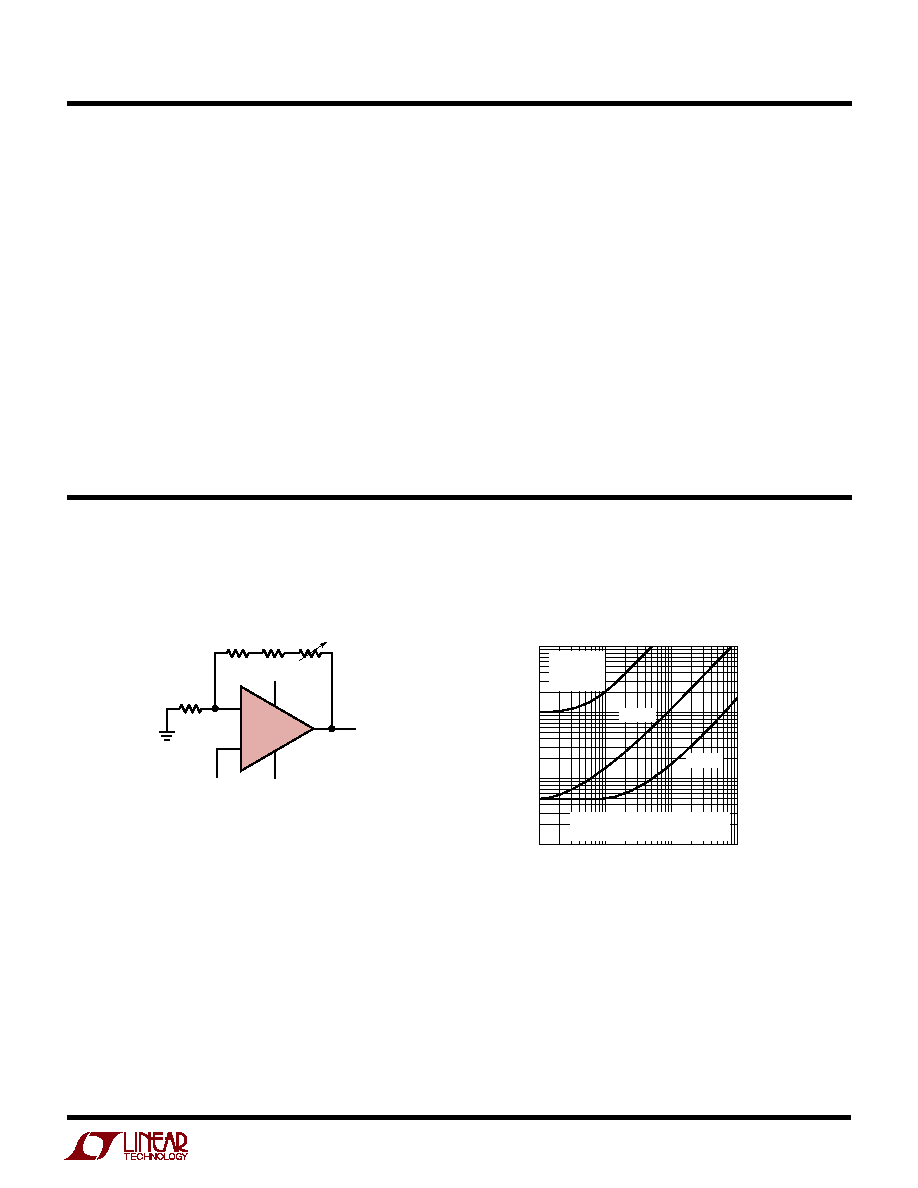
Offset Voltage Adjustment
The input offset voltage of the LT1007/LT1037 and its drift
with temperature, are permanently trimmed at wafer
testing to a low level. However, if further adjustment of
V
OS
is necessary, the use of a 10k
nulling potentiometer
will not degrade drift with temperature. Trimming to a
value other than zero creates a drift of (V
OS
/ 300)
µ
V/
∞
C,
e.g., if V
OS
is adjusted to 300
µ
V, the change in drift will be
1
µ
V/
∞
C (Figure 1).
The adjustment range with a 10k
pot is approximately
±
2.5mV. If less adjustment range is needed, the sensitivity
and resolution of the nulling can be improved by using a
smaller pot in conjunction with fixed resistors. The ex-
ample has an approximate null range of
±
200
µ
V
(Figure 2).
Offset Voltage and Drift
Thermocouple effects, caused by temperature gradients
across dissimilar metals at the contacts to the input
terminals, can exceed the inherent drift of the amplifier
unless proper care is exercised. Air currents should be
minimized, package leads should be short, the two input
leads should be close together and maintained at the same
temperature.
The circuit shown to measure offset voltage is also used
as the burn-in configuration for the LT1007/LT1037, with
the supply voltages increased to
±
20V (Figure 3).
Figure 2. Improved Sensitivity Adjustment
1007/37 F02
1k
4.7k
OUTPUT
8
7 6
4
1
2
3
15V
≠15V
≠
+
LT1007
LT1037
4.7k
1007/37 F01
10k
OUTPUT
INPUT
8
7
6
4
1
2
3
15V
≠15V
≠
+
LT1007
LT1037
Figure 1. Standard Adjustment
Unity-Gain Buffer Application (LT1007 Only)
When R
F
100
and the input is driven with a fast, large-
signal pulse (>1V), the output waveform will look as
shown in the pulsed operation diagram (Figure 4).
During the fast feedthrough-like portion of the output, the
input protection diodes effectively short the output to the
input and a current, limited only by the output short-circuit
protection, will be drawn by the signal generator. With
R
F
500
, the output is capable of handling the current
requirements (I
L
20mA at 10V) and the amplifier stays
in its active mode and a smooth transition will occur.
1007/37 F04
LT1007
≠
+
R
F
OUTPUT
2.8V/
µ
s
Figure 4. Pulsed Operation
1007/37 F03
V
OUT
V
OUT
=
1000V
OS
*RESISTORS MUST HAVE LOW
THERMOELECTRIC POTENTIAL
7
6
4
2
3
15V
≠15V
≠
+
LT1007
LT1037
50k*
100
*
50k*
Figure 3. Test Circuit for Offset Voltage and
Offset Voltage Drift with Temperature

10
LT1007/LT1037
100737fb
APPLICATIO
N
S I
N
FOR
M
ATIO
N
W
U
U
U
As with all operational amplifiers when R
F
> 2k, a pole will
be created with R
F
and the amplifier's input capacitance,
creating additional phase shift and reducing the phase
margin. A small capacitor (20pF to 50pF) in parallel with R
F
will eliminate this problem.
Noise Testing
The 0.1Hz to 10Hz peak-to-peak noise of the LT1007/
LT1037 is measured in the test circuit shown (Figure 5a).
The frequency response of this noise tester (Figure 5b)
indicates that the 0.1Hz corner is defined by only one zero.
The test time to measure 0.1Hz to 10Hz noise should not
exceed ten seconds, as this time limit acts as an additional
zero to eliminate noise contributions from the frequency
band below 0.1Hz.
Measuring the typical 60nV peak-to-peak noise perfor-
mance of the LT1007/LT1037 requires special test
precautions:
1. The device should be warmed up for at least five
minutes. As the op amp warms up, its offset voltage
changes typically 3
µ
V due to its chip temperature
increasing 10
∞
C to 20
∞
C from the moment the power
supplies are turned on. In the ten-second measurement
interval these temperature-induced effects can easily
exceed tens of nanovolts.
2. For similar reasons, the device must be well shielded
from air currents to eliminate the possibility of thermo-
electric effects in excess of a few nanovolts, which
would invalidate the measurements.
3. Sudden motion in the vicinity of the device can also
"feedthrough" to increase the observed noise.
A noise voltage density test is recommended when mea-
suring noise on a large number of units. A 10Hz noise
voltage density measurement will correlate well with a
0.1Hz to 10Hz peak-to-peak noise reading since both
results are determined by the white noise and the location
of the 1/f corner frequency.
Current noise is measured in the circuit shown in Figure 6
and calculated by the following formula:
i
e
nV
M
n
no
=
( )
-
(
)
( )( )
2
2
1 2
130
101
1
101
∑
/
FREQUENCY (Hz)
100
90
80
70
60
50
40
30
0.01
1
10
100
1007/37F05b
0.1
GAIN (dB)
1007/37 F05a
10
0.1
µ
F
4.7
µ
F
VOLTAGE GAIN
= 50,000
24.3k
100k
≠
+
≠
+
*
LT1007
LT1037
LT1001
2k
4.3k
110k
100k
SCOPE
◊
1
R
IN
= 1M
*DEVICE UNDER TEST
NOTE: ALL CAPACITOR VALUES ARE FOR
NONPOLARIZED CAPACITORS ONLY
2.2
µ
F
0.1
µ
F
22
µ
F
Figure 5a. 0.1Hz to 10Hz Noise Test Circuit
1007/37 F06
100
100k
≠
+
LT1007
LT1037
500k
500k
e
no
Figure 6
Figure 5b. 0.1Hz to 10Hz Peak-to-
Peak Noise Tester Frequency
Response
11
LT1007/LT1037
100737fb
The LT1007/LT1037 achieve their low noise, in part, by
operating the input stage at 120
µ
A versus the typical 10
µ
A
of most other op amps. Voltage noise is inversely propor-
tional while current noise is directly proportional to the
square root of the input stage current. Therefore, the
LT1007/LT1037's current noise will be relatively high. At
low frequencies, the low 1/f current noise corner fre-
quency (
120Hz) minimizes current noise to some extent.
In most practical applications, however, current noise will
not limit system performance. This is illustrated in the
Total Noise vs Source Resistance plot in the Typical
Performance Characteristics section, where:
Total Noise = [(voltage noise)
2
+ (current noise ∑ R
S
)
2
+
(resistor noise)
2
]
1/2
Three regions can be identified as a function of source
resistance:
(i) R
S
400
. Voltage noise dominates
(ii) 400
R
S
50k at 1kHz
400
R
S
8k at 10Hz
(iii) R
S
> 50k at 1kHz
R
S
> 8k at 10Hz
Clearly the LT1007/LT1037 should not be used in region
(iii), where total system noise is at least six times higher
than the voltage noise of the op amp, i.e., the low voltage
noise specification is completely wasted.
TYPICAL APPLICATIO
N
S
U
1007/37 TA03
365
1%
15k
5%
20k
TRIM
≠
+
LT1037
2
15V
≠15V
INPUT
3
7
6
4
OUTPUT
RN60C FILM RESISTORS
340k
1%
THE HIGH GAIN AND WIDE BANDWIDTH OF THE LT1037 (AND LT1007) IS
USEFUL IN LOW FREQUENCY, HIGH CLOSED-LOOP GAIN AMPLIFIER
APPLICATIONS. A TYPICAL PRECISION OP AMP MAY HAVE AN OPEN-LOOP
GAIN OF ONE MILLION WITH 500kHz BANDWIDTH. AS THE GAIN ERROR
PLOT SHOWS, THIS DEVICE IS CAPABLE OF 0.1% AMPLIFYING ACCURACY
UP TO 0.3Hz ONLY. EVEN INSTRUMENTATION RANGE SIGNALS CAN VARY
AT A FASTER RATE. THE LT1037'S "GAIN PRECISION-BANDWIDTH
PRODUCT" IS 200 TIMES HIGHER AS SHOWN.
FREQUENCY (Hz)
0.1
0.001
GAIN ERROR (%) 0.01
0.1
1
1
10
100
TYPICAL
PRECISION
OP AMP
LT1007
LT1037
GAIN ERROR =
CLOSED-LOOP GAIN
OPEN-LOOP GAIN
Gain 1000 Amplifier with 0.01% Accuracy, DC to 5Hz
Gain Error vs Frequency
Closed-Loop Gain = 1000
}
Resistor noise
dominates
}
Current noise
dominates
APPLICATIO
N
S I
N
FOR
M
ATIO
N
W
U
U
U

12
LT1007/LT1037
100737fb
TYPICAL APPLICATIO
N
S
U
Infrared Detector Preamplifier
1007/37 TA08
IR RADIATION
OPTICAL
CHOPPER
≠
+
LT1007
50mA
15V
6
4
7
3
2
OUTPUT TO
DEMODULATOR
SYNCHRONOUS
CHOPPED DETECTOR
OUTPUT
PHOTOCONDUCTIVE
INFRARED DETECTOR
HgCdTe type
INFRA-RED ASSOCIATES, INC.
100
µ
F
392k*
15V
≠15V
+
+
100
µ
F
10
µ
F
+
392
*
392
*
267
*
2N2219A
33
10
1k
+
100
µ
F
13
AT 77
∞
K
*1% METAL FILM
Precision Amplifier Drives 300
Load to
±
10V
1007/37 TA05
365
1%
20k
5%
10k
TRIM
≠
+
LT1037
≠
+
LT1007
2
INPUT
3
2
3
6
6
OUTPUT
±
10V
15
5%
15
5%
R
L
300
340k
1%
THE ADDITION OF THE LT1007 DOUBLES THE AMPLIFIER'S OUTPUT DRIVE
TO
±
33mA. GAIN ACCURACY IS 0.02%, SLIGHTLY DEGRADED COMPARED
TO ABOVE BECAUSE OF SELF-HEATING OF THE LT1037 UNDER LOAD.
Microvolt Comparator with Hysteresis
1007/37 TA04
OUTPUT
POSITIVE FEEDBACK TO ONE OF THE NULLING TERMINALS
CREATES APPROXIMATELY 5
µ
V OF HYSTERESIS.
OUTPUT CAN SINK 16mA.
INPUT OFFSET VOLTAGE IS TYPICALLY CHANGED LESS
THAN 5
µ
V DUE TO THE FEEDBACK.
7
8
6
4
2
3
INPUT
≠15V
15V
≠
+
LT1007
100M
5%
365
1%
15k
1%

13
LT1007/LT1037
100737fb
TYPICAL APPLICATIO
N
S
U
Phono Preamplifier
1007/37 TA06
100
≠
+
LT1037
MAG PHONO
INPUT
7
6
4
3
2
7.87k
15V
≠15V
OUTPUT
ALL RESISTORS METAL FILM
0.01
µ
F
0.033
µ
F
100pF
47k
100k
Tape Head Amplifier
1007/37 TA07
100
≠
+
LT1037
TAPE HEAD
INPUT
6
3
2
OUTPUT
ALL RESISTORS METAL FILM
0.01
µ
F
4.99k
316k
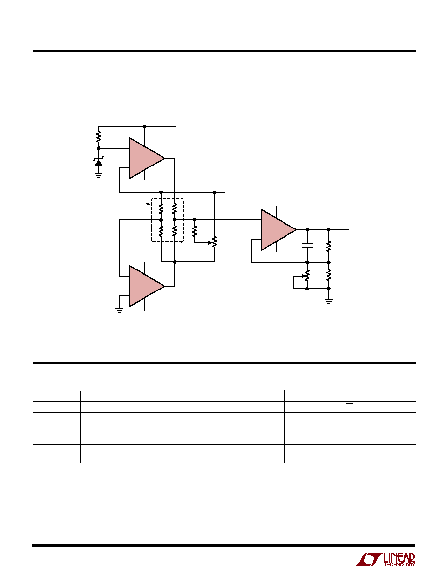
SI PLIFIED SCHE ATIC
W
W
Q1A
Q10
Q6
Q4
Q2B
Q15
Q2A
Q1B
INVERTING
INPUT (≠)
C1 = 110pF FOR LT1007
C1 = 12pF FOR LT1037
NONINVERTING
INPUT (+)
3
1
8
7
6
V
≠
V
≠
V
+
V
+
4
V
≠
1007/37 SD
V
+
OUTPUT
Q8
3.4k
3.4k
17k
17k
1.2k
750
20
20
200
50
200
200
6k
6k
80pF
20pF
C1
1.2k
Q20
130pF
Q17
Q18
Q25
Q24
Q23
Q16
Q12
Q22
Q30
Q28
Q26
Q29
Q27
450
µ
A
240
µ
A
500
µ
A
120
µ
A
240
µ
A
750
µ
A
Q19
Q11
Q13
Q7
2
Q3
Q5
Q9

14
LT1007/LT1037
100737fb
PACKAGE DESCRIPTIO
N
U
H Package
8-Lead TO-5 Metal Can (.200 Inch PCD)
(Reference LTC DWG # 05-08-1320)
J8 Package
8-Lead CERDIP (Narrow .300 Inch, Hermetic)
(Reference LTC DWG # 05-08-1110)
45
∞
TYP
0.050
(1.270)
MAX
0.016 ≠ 0.021**
(0.406 ≠ 0.533)
0.010 ≠ 0.045*
(0.254 ≠ 1.143)
SEATING
PLANE
0.040
(1.016)
MAX
0.165 ≠ 0.185
(4.191 ≠ 4.699)
GAUGE
PLANE
REFERENCE
PLANE
0.500 ≠ 0.750
(12.700 ≠ 19.050)
0.305 ≠ 0.335
(7.747 ≠ 8.509)
0.335 ≠ 0.370
(8.509 ≠ 9.398)
DIA
0.200
(5.080)
TYP
0.027 ≠ 0.045
(0.686 ≠ 1.143)
0.027 ≠ 0.034
(0.686 ≠ 0.864)
0.110 ≠ 0.160
(2.794 ≠ 4.064)
INSULATING
STANDOFF
H8(TO-5) 0.200 PCD 0595
LEAD DIAMETER IS UNCONTROLLED BETWEEN THE REFERENCE PLANE
AND 0.045" BELOW THE REFERENCE PLANE
FOR SOLDER DIP LEAD FINISH, LEAD DIAMETER IS
0.016 ≠ 0.024
(0.406 ≠ 0.610)
*
**
J8 1298
0.014 ≠ 0.026
(0.360 ≠ 0.660)
0.200
(5.080)
MAX
0.015 ≠ 0.060
(0.381 ≠ 1.524)
0.125
3.175
MIN
0.100
(2.54)
BSC
0.300 BSC
(0.762 BSC)
0.008 ≠ 0.018
(0.203 ≠ 0.457)
0
∞
≠ 15
∞
0.005
(0.127)
MIN
0.405
(10.287)
MAX
0.220 ≠ 0.310
(5.588 ≠ 7.874)
1
2
3
4
8
7
6
5
0.025
(0.635)
RAD TYP
0.045 ≠ 0.068
(1.143 ≠ 1.727)
FULL LEAD
OPTION
0.023 ≠ 0.045
(0.584 ≠ 1.143)
HALF LEAD
OPTION
CORNER LEADS OPTION
(4 PLCS)
0.045 ≠ 0.065
(1.143 ≠ 1.651)
NOTE: LEAD DIMENSIONS APPLY TO SOLDER DIP/PLATE
OR TIN PLATE LEADS
OBSOLETE PACKAGES
15
LT1007/LT1037
100737fb
Information furnished by Linear Technology Corporation is believed to be accurate and reliable.
However, no responsibility is assumed for its use. Linear Technology Corporation makes no represen-
tation that the interconnection of its circuits as described herein will not infringe on existing patent rights.
PACKAGE DESCRIPTIO
N
U
N8 Package
8-Lead PDIP (Narrow .300 Inch)
(Reference LTC DWG # 05-08-1510)
S8 Package
8-Lead Plastic Small Outline (Narrow .150 Inch)
(Reference LTC DWG # 05-08-1610)
N8 1098
0.100
(2.54)
BSC
0.065
(1.651)
TYP
0.045 ≠ 0.065
(1.143 ≠ 1.651)
0.130
±
0.005
(3.302
±
0.127)
0.020
(0.508)
MIN
0.018
±
0.003
(0.457
±
0.076)
0.125
(3.175)
MIN
1
2
3
4
8
7
6
5
0.255
±
0.015*
(6.477
±
0.381)
0.400*
(10.160)
MAX
0.009 ≠ 0.015
(0.229 ≠ 0.381)
0.300 ≠ 0.325
(7.620 ≠ 8.255)
0.325
+0.035
≠0.015
+0.889
≠0.381
8.255
(
)
*THESE DIMENSIONS DO NOT INCLUDE MOLD FLASH OR PROTRUSIONS.
MOLD FLASH OR PROTRUSIONS SHALL NOT EXCEED 0.010 INCH (0.254mm)
0.016 ≠ 0.050
(0.406 ≠ 1.270)
0.010 ≠ 0.020
(0.254 ≠ 0.508)
◊
45
∞
0
∞
≠ 8
∞
TYP
0.008 ≠ 0.010
(0.203 ≠ 0.254)
SO8 1298
0.053 ≠ 0.069
(1.346 ≠ 1.752)
0.014 ≠ 0.019
(0.355 ≠ 0.483)
TYP
0.004 ≠ 0.010
(0.101 ≠ 0.254)
0.050
(1.270)
BSC
1
2
3
4
0.150 ≠ 0.157**
(3.810 ≠ 3.988)
8
7
6
5
0.189 ≠ 0.197*
(4.801 ≠ 5.004)
0.228 ≠ 0.244
(5.791 ≠ 6.197)
DIMENSION DOES NOT INCLUDE MOLD FLASH. MOLD FLASH
SHALL NOT EXCEED 0.006" (0.152mm) PER SIDE
DIMENSION DOES NOT INCLUDE INTERLEAD FLASH. INTERLEAD
FLASH SHALL NOT EXCEED 0.010" (0.254mm) PER SIDE
*
**
16
LT1007/LT1037
100737fb
LT/CPI 1101 1.5K REV B ∑ PRINTED IN USA
©
LINEAR TECHNOLOGY CORPORATION 1985
Strain Gauge Signal Conditioner with Bridge Excitation
6
4
7
3
2
7.5V
7.5V
≠7.5V
6
4
7
≠7.5V
1007/37 TA09
≠
+
LT1007
≠
+
LT1007
6
4
7
3
3
2
2
350
BRIDGE
OUTPUT
0V TO 10V
301k*
301k*
GAIN
TRIM
50k
ZERO
TRIM
10k
REFERENCE
OUT
1
µ
F
15V
≠15V
499
*
5k
2.5V
LT1009
≠
+
LT1007
*RN60C FILM RESISTOR
THE LT1007 IS CAPABLE OF PROVIDING EXCITATION CURRENT
DIRECTLY TO BIAS THE 350
BRIDGE AT 5V. WITH ONLY 5V ACROSS
THE BRIDGE (AS OPPOSED TO THE USUAL 10V) TOTAL POWER
DISSIPATION AND BRIDGE WARM-UP DRIFT IS REDUCED. THE BRIDGE
OUTPUT SIGNAL IS HALVED, BUT THE LT1007 CAN AMPLIFY THE
REDUCED SIGNAL ACCURATELY.
RELATED PARTS
PART NUMBER
DESCRIPTION
COMMENTS
LT1028
Ultralow Noise Precision Op Amp
Lowest Noise 0.85nV/
Hz
LT1115
Ultralow Noise, Low distortion Audio Op Amp
0.002% THD, Max Noise 1.2mV/
Hz
LT1124/LT1125
Dual/Quad Low Noise, High Speed Precision Op Amps
Similar to LT1007
LT1126/LT1127
Dual/Quad Decompensated Low Noise, High Speed Precision Op Amps
Similar to LT1037
LT1498/LT1499
10MHz, 5V/
µ
s, Dual/Quad Rail-to-Rail Input and Output
Precision C-Load
TM
Op Amps
C-Load is a trademark of Linear Technology Corporation.
U
TYPICAL APPLICATIO
Linear Technology Corporation
1630 McCarthy Blvd., Milpitas, CA 95035-7417
(408) 432-1900
q
FAX: (408) 434-0507
q
www.linear.com