 | –≠–ª–µ–∫—Ç—Ä–æ–Ω–Ω—ã–π –∫–æ–º–ø–æ–Ω–µ–Ω—Ç: LT1020ISW | –°–∫–∞—á–∞—Ç—å:  PDF PDF  ZIP ZIP |
1
LT1020
sn1020 1020fcs
Micropower Regulator
and Comparator
s
Input Voltage Range: 4.5V to 36V
s
40
µ
A Supply Current
s
125mA Output Current
s
2.5V Reference Voltage
s
Reference Output Sources 1mA and Sinks 0.5mA
s
Dual Output Comparator
s
Comparator Sinks 10mA
s
Dropout Detector
s
0.2V Dropout Voltage
s
Thermal Limiting
s
Available in SO Package
s
Battery Systems
s
Battery Backup Systems
s
Portable Terminals
s
Portable Instruments
The LT
Æ
1020 is a combination micropower positive regu-
lator and free collector comparator on a single monolithic
chip. With only 40
µ
A supply current, the LT1020 can
supply over 125mA of output current. Input voltage range
is from 4.5V to 36V and dropout voltage is 0.6V at 125mA.
Dropout voltage decreases with lower load currents. Also
included on the chip is a class B output 2.5V reference that
can either source or sink current. A dropout detector
provides an output current to indicate when the regulator
is about to drop out of regulation.
The dual output comparator can be used as a comparator
for system or battery monitoring. For example, the com-
parator can be used to warn of low system voltage while
the dropout detector shuts down the system to prevent
abnormal operation. Frequency compensation of the com-
parator for amplifier applications can be obtained by
adding external output capacitance. Dual output or posi-
tive and negative regulators can also be made.
The 2.5V reference will source or sink current. This allows
it to be used as a supply splitter or auxiliary output.
5V Regulator
Dropout Voltage and Supply Current
+
V
IN
> 5.2V
I
Q
= 40
µ
A
10
µ
F
10
µ
F
0.001
µ
F
1M
1M
5V
2
11
3
9
V
IN
V
OUT
FB
GND
+
LT1020
1020 TA01
OUTPUT CURRENT (mA)
0.1
0.01
DROPOUT VOLTAGE (V)
0.1
1
10
1000
1020 TA02
1
100
0.1
1
10
SUPPLY CURRENT (mA)
FEATURES
DESCRIPTIO
U
APPLICATIO S
U
TYPICAL APPLICATIO
U
, LTC and LT are registered trademarks of Linear Technology Corporation.
2
LT1020
sn1020 1020fcs
A
U
G
W
A
W
U
W
A
R
BSOLUTE
XI
TI
S
Input Voltage .......................................................... 36V
NPN Collector Voltage ............................................ 36V
PNP Collector Voltage ............................. Supply ≠ 36V
Output Short Circuit Duration ......................... Indefinite
Power Dissipation .............................. Internally Limited
Storage Temperature Range ................ ≠ 65
∞
C to 150
∞
C
Operating Temperature Range
LT1020C ............................................. 0
∞
C to 100
∞
C
LT1020I ........................................ ≠ 40
∞
C to 100
∞
C
LT1020M (OBSOLETE) .................. ≠ 55
∞
C to 125
∞
C
Lead Temperature (Soldering, 10 sec).................. 300
∞
C
W
U
U
PACKAGE/ORDER I FOR ATIO
T
JMAX
= 110
∞
C,
JA
= 130
∞
C/W
T
JMAX
= 110
∞
C,
JA
= 150
∞
C/W
ORDER PART
NUMBER
LT1020CJ
LT1020IJ
LT1020MJ
ORDER PART
NUMBER
LT1020CSW
LT1020ISW
1
2
3
4
5
6
7
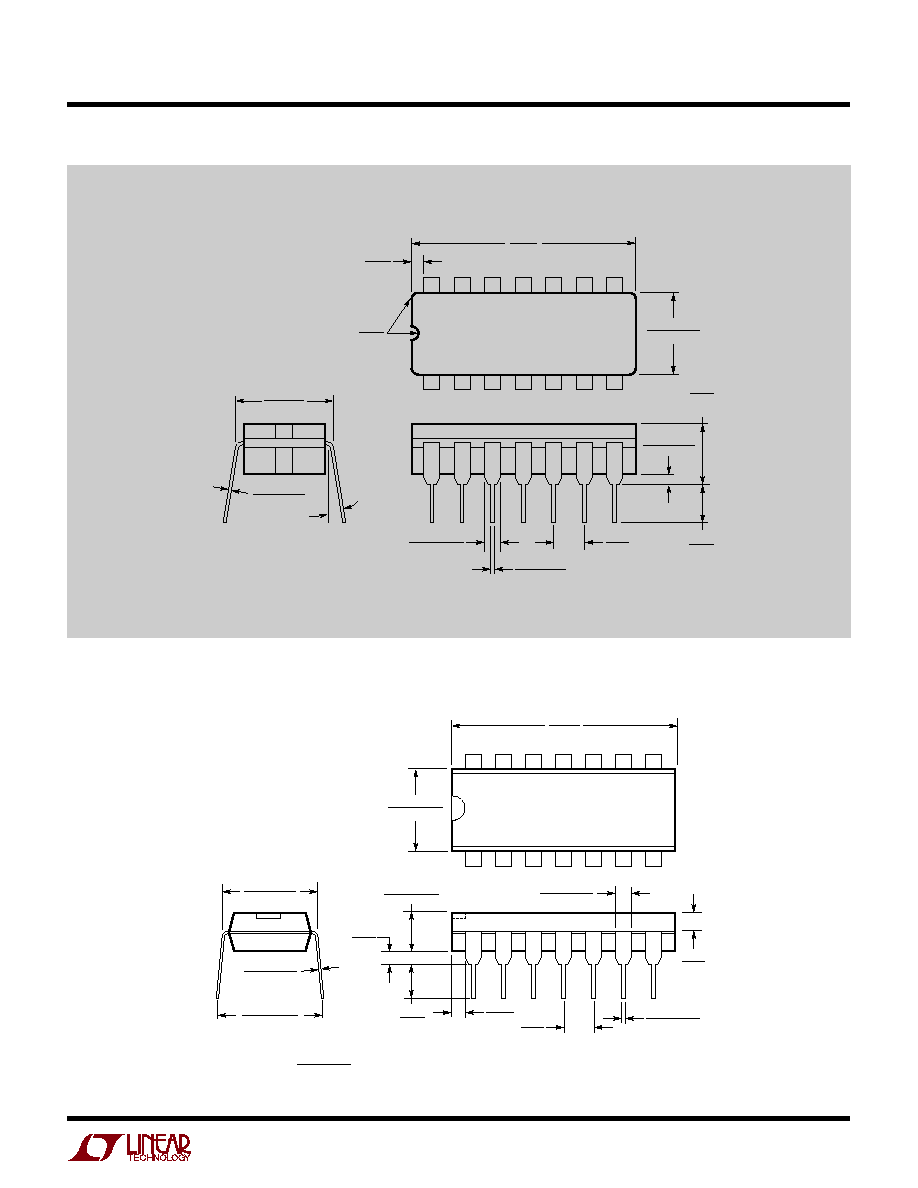
TOP VIEW
N PACKAGE
14-LEAD PDIP
14
13
12
11
10
9
8
NC
V
OUT
V
IN
REF OUT
COMP PNP
COMP NPN
+INPUT
NC
SHUTDOWN
FEEDBACK
GND
≠INPUT
DROPOUT
DETECTOR
CURRENT
LIMIT
TOP VIEW
SW PACKAGE
16-LEAD PLASTIC (WIDE) SO
1
2
3
4
5
6
7
8
16
15
14
13
12
11
10
9
NC
V
OUT
VI
N
REF OUT
COMP PNP
COMP NPN
+INPUT
NC
NC
SHUTDOWN
FEEDBACK
GND
≠INPUT
NC
DROPOUT
DETECTOR
CURRENT
LIMIT
(Note 1)
J PACKAGE 14-LEAD CERDIP
T
JMAX
= 150
∞
C,
JA
= 80
∞
C/W
LT1020CN
LT1020IN
OBSOLETE PACKAGE
Consider the N14 Package for Alternate Source
T
J
= 25
∞
C
ELECTRICAL C
C
HARA TERISTICS
Consult LTC Marketing for parts specified with wider operating temperature ranges.
PARAMETER
CONDITIONS
MIN
TYP
MAX
UNITS
Reference
Reference Voltage
4.5V
V
IN
36V
2.46
2.50
2.54
V
Line Regulation
4.5V
V
IN
36V
0.01
0.015
%/V
Load Regulation
≠ 0.5mA
I
REF
1mA, V
IN
= 12V
0.2
0.3
%
Output Source Current
V
IN
= 5V
1
4
mA
Output Sink Current
V
IN
= 5V
0.5
2
mA
Temperature Stability
1
%
Regulator
Supply Current
V
IN
= 6V, I
OUT
100
µ
A
45
80
µ
A
V
IN
= 36V, I
OUT
100
µ
A
75
120
µ
A
V
IN
= 12V, I
OUT
= 125mA
11
20
mA
Output Current
(V
IN
≠ V
OUT
)
1V, V
IN
6V
125
mA
Load Regulation
(V
IN
≠ V
OUT
)
1V, V
IN
6V
0.2
0.5
%
Line Regulation
6V
V
IN
36V
0.01
0.015
%/V
Dropout Voltage
I
OUT
= 100
µ
A
0.02
0.05
V
I
OUT
= 125mA
0.4
0.65
V
3
LT1020
sn1020 1020fcs
T
J
= 25
∞
C
ELECTRICAL C
C
HARA TERISTICS
PARAMETER
CONDITIONS
MIN
TYP
MAX
UNITS
Regulator
Feedback Sense Voltage
V
IN
= 12V
2.44
2.5
2.56
V
Dropout Detector Current
V
OUT
= ≠ 0.05V, I
OUT
= 500
µ
A
3
20
µ
A
Feedback Bias Current
15
40
nA
Minimum Load Current
V
IN
= 36V
1
5
µ
A
Short-Circuit Current
V
IN
= 36V
300
400
mA
Pins 9 and 10 Shorted, V
IN
= 4.5V
3
30
mA
Comparator
Offset Voltage
0V
V
CM
35V, V
IN
= 36V
3
7
mV
Bias Current
0V
V
CM
35V, V
IN
= 36V
15
40
nA
Offset Current
0V
V
CM
35V, V
IN
= 36V
4
15
nA
Gain-NPN Pull-Down
V
OUT
= 29V, R
L
= 20k
2000
10000
V/ V
Common Mode Rejection
0V
V
CM
35V, V
IN
= 36V
80
94
dB
Power Supply Rejection
4.5V
V
S
36V
80
96
dB
Output Sink Current
V
IN
= 4.5V
10
18
mA
NPN Saturation Voltage
I
OUT
= 1mA
0.4
0.6
V
Output Source Current
60
200
µ
A
Input Voltage Range
0
V
IN
≠ 1
V
Response Time
5
µ
s
Leakage Current (NPN)
2
µ
A
The
q
denotes the specifications which apply over the full operating temperature range, otherwise specifications are at T
J
= 25
∞
C.
PARAMETER
CONDITIONS
MIN
TYP
MAX
UNITS
Reference
Reference Voltage
4.5V
V
IN
36V
q
2.40
2.50
2.55
V
Line Regulation
4.5V
V
IN
36V
q
0.01
0.02
%/V
Load Regulation
≠ 0.5mA
I
REF
1mA, V
IN
= 12V
q
0.3
0.4
%
Output Source Current
V
IN
= 5V
q
1
mA
Output Sink Current
V
IN
= 5V
q
0.5
mA
Regulator
Supply Current
V
IN
= 6V, I
OUT
100
µ
A
q
65
95
µ
A
V
IN
= 36V, I
OUT
100
µ
A
q
85
120
µ
A
V
IN
= 12V, I
OUT
= 125mA
q
11
20
mA
Output Current
(V
IN
≠ V
OUT
)
1V, V
IN
6V
q
125
mA
Load Regulation
(V
IN
≠ V
OUT
)
1V, V
IN
6V
q
1
%
Line Regulation
6V
V
IN
36V
q
0.02
%/ V
Dropout Voltage
I
OUT
= 100
µ
A
q
0.06
V
I
OUT
= 125mA
q
0.85
V
Feedback Sense Voltage
V
IN
= 12V
q
2.38
2.5
2.57
V
Dropout Detector Current
V
OUT
= ≠ 0.05V, I
OUT
= 500
µ
A
q
3
µ
A
Feedback Bias Current
q
50
nA
Minimum Load Current
V
IN
= 36V
q
50
µ
A
Short-Circuit Current
V
IN
= 36V
q
300
400
mA
Pins 9 and 10 Shorted, V
IN
= 4.5V
q
2.5
30
mA
Comparator
Offset Voltage
0V
V
CM
35V, V
IN
= 36V
q
10
mV
Bias Current
0V
V
CM
35V, V
IN
= 36V (Note 2)
q
15
60
nA
4
LT1020
sn1020 1020fcs
OUTPUT CURRENT (mA)
OUTPUT VOLTAGE CHANGE (%)
0.3
0.2
0.1
0
≠0.1
≠0.2
≠0.3
0.1
10
100
1000
1020 G01
1
T
J
= ≠55
∞
C
T
J
= 25
∞
C
T
J
= 125
∞
C
PRELOAD = 100
µ
A
Regulator Short-Circuit Current
TEMPERATURE (
∞
C)
≠50
SHORT-CIRCUIT CURRENT (mA)
350
300
250
200
150
100
50
0
1020 G03
30
150
≠10
70
110
CURRENT LIMIT TIED TO GROUND
Regulator Load Regulation
Dropout Voltage
Dropout Voltage
REGULATOR OUTPUT CURRENT (mA)
0.1
0.01
INPUT/OUTPUT DIFFERENTIAL (V)
0.1
1
1
10
100
1020 G06
I DROPOUT DETECTOR = 0.1% I
OUT
I DROPOUT DETECTOR = 1% I
OUT
Dropout Voltage
REGULATOR OUTPUT CURRENT (mA)
SUPPLY CURRENT (mA)
100
10
1
0.1
0.01
0.1
10
100
1000
1020 G02
1
T
J
= ≠55
∞
C TO 125
∞
C
Supply Current
REGULATOR OUTPUT CURRENT (mA)
0.1
0.01
REGULATOR INPUT/OUTPUT DIFFERENTIAL (V)
0.1
1
10
1000
1020 G04
1
100
V
OUT
= 100mV
REGULATOR OUTPUT CURRENT (mA)
0.1
0.01
REGULATOR INPUT/OUTPUT DIFFERENTIAL (V)
0.1
1
10
1000
1020 G05
1
100
DROPOUT DETECTOR = 5
µ
A
PARAMETER
CONDITIONS
MIN
TYP
MAX
UNITS
Comparator
Offset Current
0V
V
CM
35V, V
IN
= 36V
q
20
nA
Gain-NPN Pull-Down
V
OUT
= 29V, R
L
= 20k
q
1000
V/ V
Common Mode Rejection
0V
V
CM
35V, V
IN
= 36V
q
80
dB
Power Supply Rejection
4.5V
V
IN
36V
q
80
dB
Output Sink Current
V
IN
= 4.5V (Note 3)
q
5
10
mA
Output Source Current
q
40
120
µ
A
Input Voltage Range
q
0
V
IN
≠ 1
V
Leakage Current (NPN)
V
IN
= 36V
q
8
µ
A
TYPICAL PERFOR A CE CHARACTERISTICS
U
W
ELECTRICAL CHARACTERISTICS
The
q
denotes the specifications which apply over the full operating
temperature range, otherwise specifications are at T
J
= 25
∞
C.
Note 1: Absolute Maximum Ratings are those values beyond which the life
of a device may be impaired.
Note 2: For 0V
V
CM
0.1V and T > 85
∞
C I
BIAS(MAX)
is 100nA.
Note 3: For T
A
≠ 40
∞
C output I
SINK(MIN)
is 2.5mA.
5
LT1020
sn1020 1020fcs
RIPPLE FREQUENCY (Hz)
10
RIPPLE REJECTION (dB)
70
65
60
55
50
45
40
35
30
100
1k
1020 G10
10k
100k
I
OUT
= 100mA
I
OUT
= 10mA
I
OUT
= 1mA
V
IN
= 100VDC, 1V
P-P
V
OUT
= 5V
C
OUT
= 10
µ
F
Regulator Ripple Rejection
REGULATOR INPUT/OUTPUT DIFFERENTIAL (V)
1
SUPPLY CURRENT (mA)
10
1
0.1
0.01
5
1020 G11
I
OUT
= 100mA
10
15
20
25
I
OUT
= 1mA
I
OUT
= 10mA
V
OUT
= 5V
T
J
= ≠55
∞
C TO 125
∞
C
Supply Current
REGULATOR OUTPUT CURRENT (mA)
0.1
FEEDBACK PIN CURRENT (nA)
40
35
30
25
20
15
10
5
0
1
10
1020 G15
100
1000
T
J
= 125
∞
C
T
J
= 25
∞
C
T
J
= ≠55
∞
C
Supply Current at Dropout
Feedback Pin Current
Comparator Input Bias Current
COMMON MODE VOLTAGE (V)
REFERRED TO PIN 9 (GND)
≠1.0
INPUT BIAS CURRENT (nA)
100
90
80
70
60
50
40
30
20
10
0
0.6
1020 G14
≠0.6
≠0.2
0.2
1.0
T
J
= 125
∞
C
GND
T
J
= 25
∞
C
T
J
= ≠55
∞
C
Reference Regulation
REGULATOR INPUT/OUTPUT DIFFERENTIAL (V)
0
DROPOUT DETECTOR CURRENT (
µ
A)
1000
100
10
1
0.1
1020 G08
I
OUT
= 100mA
0.2
0.3
0.4
0.6
0.5
I
OUT
= 25mA
I
OUT
= 1mA
I
OUT
= 5mA
REGULATOR OUTPUT CURRENT (mA)
0.1
DROPOUT DETECTOR CURRENT (
µ
A)
1
10
100
10
1000
1020 G07
0.01
100
V
DIFF
= 500mV
V
DIFF
= 1V
Dropout Detector Current
Dropout Detector Current
TEMPERATURE (
∞
C)
90
1
10
100
110
130
1020 G09
MINIMUM LOAD CURRENT (
µ
A)
70
150
80
100
120
140
Regulator Minimum Load Current
REGULATOR INPUT/OUTPUT DIFFERENTIAL (V)
0
SUPPLY CURRENT (mA)
10
1
0.1
0.01
0.1
1020 G12
I
OUT
= 100mA
0.2
0.3
0.4
0.6
0.5
I
OUT
= 10mA
I
OUT
= 1mA
T
J
= ≠55
∞
C TO 125
∞
C
REFERENCE OUTPUT CURRENT (mA)
≠1.5
REFERENCE VOLTAGE CHANGE (mV)
≠1.0
0
1.0
1.5
1020 G13
4
3
2
1
0
≠1
≠2
≠3
≠4
≠0.5
0.5
TYPICAL PERFOR A CE CHARACTERISTICS
U
W
6
LT1020
sn1020 1020fcs
Pins 1, 14: No Internal Connection.
Pin 2: Regulator Output. Main output, requires 10
µ
F
output capacitor. Can be shorted to V
IN
or ground without
damaging the device.
Pin 3: Input Supply. Bypass with 10
µ
F capacitor. Must
always be more positive than ground.
Pin 4: Reference. 2.5V can source or sink current. May be
shorted to ground or up to 5V. Voltages in excess of 5V can
damage the device.
Pin 5: Comparator PNP Output. Open Collector PNP
Output. Pull-up current source for the comparator. May be
connected to any voltage from V
IN
to 36V more negative
than V
IN
(operates below ground). Short-circuit protected.
For example, if V
IN
is 6V then pin 5 will operate to ≠ 30V.
Pin 6: Comparator NPN Output. Open Collector NPN
Output. May be connected to any voltage from ground to
36V more positive than ground (operates above V
IN
).
Short-circuit protected.
Pins 7, 8: Comparator Inputs. Operates from ground to
V
IN
≠ 1V. Comparator inputs will withstand 36V even with
V
IN
of 0V.
Pin 9: Ground.
Pin 10: Current Limit. Connecting this pin to ground
decreases the regulator current limit to 3mA minimum.
Leave open when not used.
Pin 11: Feedback. This is the feedback point of the regu-
lator. When operating, it is nominally at 2.5V. Optimum
source resistance is 200k to 500k. The feedback pin
should not be driven below ground or more positive than
5V.
Pin 12: Shutdown. Turns output off.
Pin 13: Dropout Detector. This pin acts like a current
source from V
IN
which turns on when the output transistor
goes into saturation. The magnitude of the current de-
pends on the magnitude of the output current and the
input/output voltage differential. Pin current ranges from
5
µ
A to about 300
µ
A.
INPUT VOLTAGE (V)
1
OUTPUT VOLTAGE (V)
0
1020 G17
3
5
7
5.5
5.0
4.5
4.0
3.5
3.0
2.5
2.0
0
2
4
6
8
R
L
= 500
R
L
= 50
NO LOAD
V
OUT
= 5V
Regulator Thermal Regulation
TIME (ms)
0
OUTPUT
CURRENT (mA)
0.1
140
1020 G16
20 40
80
180
V
IN
= 15V
V
OUT
= 5V
60
0
≠0.1
0
50
OUTPUT VOLTAGE
CHANGE (%)
100 120
160
LT1020 Turn-On Characteristic
TYPICAL PERFOR A CE CHARACTERISTICS
U
W
U
U
U
PI FU CTIO S
7
LT1020
sn1020 1020fcs
The LT1020 is especially suited for micropower system
applications. For example, the comparator section of the
LT1020 may be used as a battery checker to provide an
indication of low battery. The dropout detector can shut
down the system when the battery voltage becomes too
low to regulate. Another type of system application for the
LT1020 would be to generate the equivalent of split
supplies from a single power input. The regulator section
provides regulated output voltage and the reference, which
can both source and sink current, is then an artificial
system ground providing a split supply for the system.
For many applications the comparator can be frequency
compensated to operate as an amplifier. Compensation
values for various gains are given in the data sheet. The
comparator gain is purposely low to make it easier to
frequency compensate as an amplifier. Two outputs are
available on the comparator, the NPN output is capable of
sinking 10mA and can drive loads connected to voltages
in excess of the positive power supply. This is useful for
driving switches or linear regulators from a higher input
voltage. The PNP output, which is capable of sourcing
100
µ
A can drive loads below ground. It can be used to
make negative regulators with the addition of an external
pass transistor. Both outputs can be tied together to
provide an output that swings from rail-to-rail for com-
parator or amplifier applications. Although it is not speci-
fied, the gain for the PNP output is about 500 to 1000.
If the PNP output is being used, to maximize the gain a 1
µ
A
to 5
µ
A load should be placed upon the NPN output
collector. This is easily done by connecting a resistor
between the NPN collector and the reference output.
(Providing this operating current to the NPN side in-
creases the internal emitter base voltages and maximizes
the gain of the PNP stage.) Without this loading on the
NPN collector, at temperatures in excess of 75
∞
C, the gain
of the PNP collector can decrease by a factor of 2 or 3.
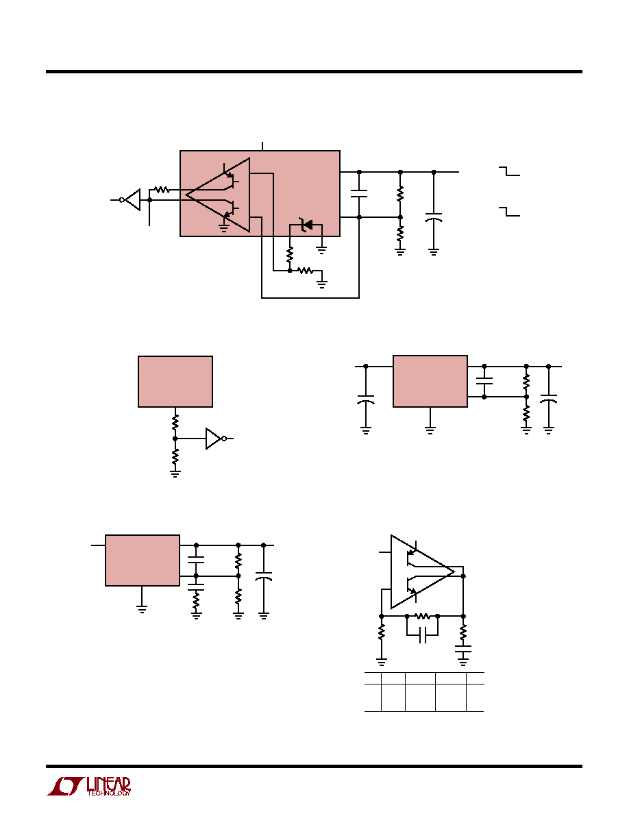
Reference
Internal to the LT1020 is a 2.5V trimmed class B output
reference. The reference was designed to be able to source
or sink current so it could be used in supply splitting
applications as well as a general purpose reference for
external circuitry. The design of the reference allows it to
source typically 4mA or 5mA and sink 2mA. The available
source and sink current decreases as temperature in-
creases. It is sometimes desirable to decrease the AC
output impedance by placing an output capacitor on them.
The reference in the LT1020 becomes unstable with large
capacitive loads placed directly on it. When using an
output capacitor, about 20
should be used to isolate the
capacitor from the reference pin. This 20
resistor can be
placed directly in series with the capacitor or alternatively
the reference line can have 20
placed in series with it and
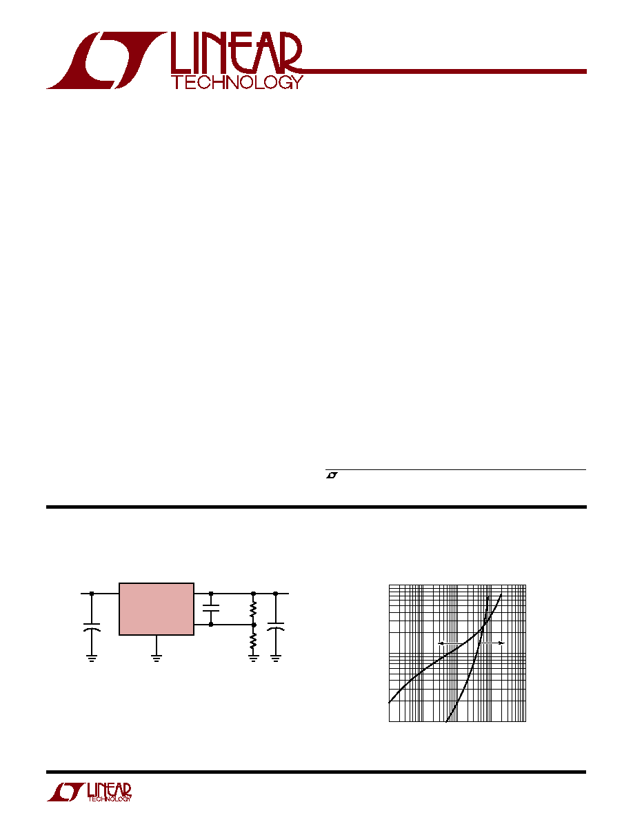
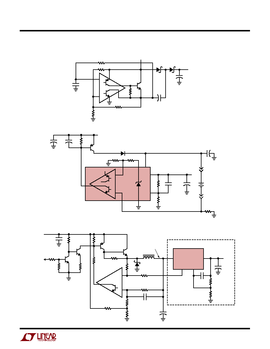
then a capacitor to ground. This is shown in Figure 1. Other
7
8
3
13
11
2
9
REF
2.5V
REF OUT
CURRENT
LIMIT
V
IN
V
OUT
DROPOUT
DETECTOR
FB
GND
INVERTING
NON-
INVERTING
NPN OUT
PNP OUT
10
4
1020 BD
≠
+
6
5
BLOCK DIAGRA
W
APPLICATIO S I FOR ATIO
W
U
U
U
8
LT1020
sn1020 1020fcs
Like most other IC regulators, a minimum load is required
on the output of the LT1020 to maintain regulation. For
most standard regulators this is normally specified at
5mA. Of course, for a micropower regulator this would be
a tremendously large current. The output current must be
large enough to absorb all the leakage current of the pass
transistor at the maximum operating temperature. It also
affects the transient response; low output currents have
long recovery times from load transients. At high operat-
ing temperatures the minimum load current increases and
having too low of a load current may cause the output to
go unregulated. Devices are tested for minimum load
current at high temperature. The output voltage setting
resistors to the feedback terminal can usually be used to
provide the minimum load current.
Frequency Compensation
The LT1020 is frequency compensated by a dominant pole
on the output. An output capacitor of 10
µ
F is usually large
enough to provide good stability. Increasing the output
capacitor above 10
µ
F further improves stability. In order
to insure stability, a feedback capacitor is needed between
the output pin and the feedback pin. This is because stray
capacitance can form another pole with the large value of
feedback resistors used with the LT1020. Also, a feedback
capacitor minimizes noise pickup and improves ripple
rejection.
With the large dynamic operating range of the output
current, 10000:1, frequency response changes widely.
Low AC impedance capacitors are needed to insure stabil-
ity. While solid tantalum are best, aluminum electrolytics
can be used but larger capacitor values may be needed.
The CURRENT LIMIT pin allows one of the internal nodes
to be rolled off with a 0.05
µ
F capacitor to ground. With this
capacitor, lower values of regulator output capacitance
can be used (down to 1
µ
F) for low (<20mA) output
currents. Values of capacitance greater than 0.05
µ
F de-
grade the transient response, so are not recommended.
If the CURRENT LIMIT pin is connected to GND, the
current limit is decreased and only a 1
µ
F output capacitor
is needed.
When bypassing the reference, a 20
resistor must be
connected in series with the capacitor.
than placing large capacitive loads on the reference, no
other precautions are necessary and the reference is
stable with nominal stray capacitances.
Figure 2. Minimizing Oscillation in Thermal Shutdown
Overload Protection
The main regulator in the LT1020 is current limited at
approximately 350mA. The current limit is stable with both
input voltage and temperature. A current limit pin, when
strapped to ground, decreases the output current. This
allows the output current to be set to a lower value than
250mA. The output current available with the current limit
pin strapped to ground is not well controlled so if precise
current limiting is desired it should be provided externally
as is shown in some of the application circuits.
If the device is overloaded for long periods of time, thermal
shutdown turns the output off. In thermal shutdown, there
may be some oscillations which can disturb external
circuitry. A diode connected between the reference and
feedback terminal provides hysteresis under thermal shut-
down, so that the device turns on and off with about a 5
second period and there are no higher frequency oscilla-
tions. This is shown in Figure 2. This diode is recom-
mended for most applications. Thermal shutdown
temperature is set at approximately 145
∞
C.
Figure 1. Bypassing Reference
+
+
REF
REF
OUTPUT
OUTPUT
20
20
10
µ
F
10
µ
F
OR
1020 F01
4
4
+
10
µ
F
0.001
µ
F
*
2
11
4
V
OUT
FB
REF
LT1020
1020 F02
* DIODE ADDS FEEDBACK
APPLICATIO S I FOR ATIO
W
U
U
U
9
LT1020
sn1020 1020fcs
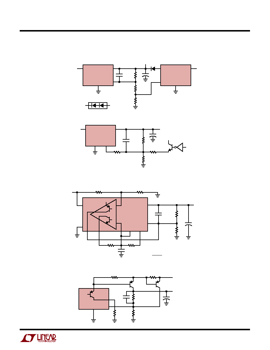
Regulator with Output Voltage Monitor
Regulator with Improved Transient Response
Driving Logic with Dropout Detector
DROPOUT
LT1020
500k
TO
2M
3M
1020 TA04
V
IN
> 5.2V
10
µ
F
0.001
µ
F
1M
1M
5V
2
11
3
9
V
IN
V
OUT
FB
GND
LT1020
1020 TA08
0.001
µ
F
22k
+
1020 TA03
5
6
100k
20k
V
OUT
0.001
µ
F
+
4
8
7
9
100k
10
µ
F
2
11
FB
5V
V
OUT
LOGIC
LOGIC
OUTPUT
LOGIC OUTPUT GOES LOW WHEN
V
OUT
DROPS BY 100mV
V
IN
V
IN
3
1M
500k
≠
+
REF
LT1020
GND
2.5V
LOGIC
OUTPUT
5V Regulator
V
IN
> 5.2V
I
Q
= 40
µ
A
10
µ
F
10
µ
F
0.001
µ
F
1M
1M
5V
2
11
3
9
V
IN
V
OUT
FB
GND
+
LT1020
1020 TA07
+
Compensating the Comparator As an Op Amp
7
≠
+
5
6
1M
C2
R2
R1
C1
AT A
V
= 100,
SLEW RATE = 0.05V/
µ
s
≠6V/
µ
s
A
V
1
10
100
R1
33
100
10k
C1
0.1
µ
F
0.047
µ
F
0.002
µ
F
C2
0.001
µ
F
≠
≠
R2
≠
100k
10k
1020 TA05
8
TYPICAL APPLICATIO S
U
10
LT1020
sn1020 1020fcs
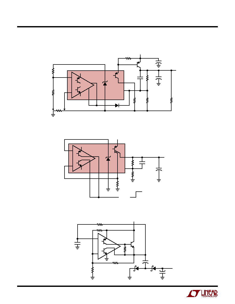
Dual Output Regulator
1020 TA12
6
1M
51k
V
OUT
0.001
µ
F
+
4
7
8
9
1M
10
µ
F
2
11
FB
5V
V
IN
3
GND
≠
+
REF
LT1020
+
10
µ
F
0.01
µ
F
+IN
≠IN
190k
50k
2N2907
12V
OUT
V
IN
12.3V
+
NC
10
µ
F
0.001
µ
F
1M
1M
5V
2
11
3
9
V
IN
V
OUT
FB
GND
LT1020
1020 TA11
13
DROP-
OUT
1M
2N3904*
TRANSISTOR USED BECAUSE OF
LOW LEAKAGE CHARACTERISTICS
*
Maintaining Lowest I
Q
at Dropout
Dual Output 150mA Regulator
Dual Output Positive Regulator
1 Amp Low Dropout Regulator
10
µ
F
0.001
µ
F
100k
2
11
3
9
V
IN
V
OUT
FB
GND
LT1020
1020 TA09
5V
51k
V
IN
> 5.2V
≠5V REG
10mA
500k
COMP
PNP
≠V
IN
7
4
6
500k
1M
8
5
500k
10
µ
F
0.001
µ
F
+INPUT
REF
OUT
COMP
NPN
≠INPUT
2N3904
+
+
10
µ
F
0.001
µ
F
100k
2
11
3
9
V
IN
V
OUT
FB
GND
LT1020
1020 TA10
5V
51k*
V
IN
> 5.2V
≠5V REG
150mA
500k
COMP
PNP
≠V
IN
7
4
6
100k
200k
8
5
500k
10
µ
F
0.001
µ
F
+INPUT
REF
OUT
COMP
NPN
≠INPUT
4.7k
0.0047
µ
F
51k*
2N3904
FOR TEMPERATURES GREATER THAN
70
∞
C, REDUCE 51k RESISTORS TO 15k.
I
Q
WILL INCREASE
*
2N3904
+
+
+
220
µ
F
0.001
µ
F
100k
2
11
3
9
V
IN
V
OUT
FB
GND
LT1020
1020 TA06
0.01
µ
F
V
OUT
5V
10k*
2.2k
10
150
*
*
V
IN
100k
C
L
FOR CURRENT LIMIT
1.5A
MUST HAVE LOW ESR.
SEVERAL 100
µ
F CAPACITORS
CAN BE PARALLELED
*
MJE2955
SEE LT1129 DATA SHEET FOR 700mA OUTPUT
TYPICAL APPLICATIO S
U
11
LT1020
sn1020 1020fcs
+
10
µ
F
0.001
µ
F
1M
50k
2
11
9
V
OUT
FB
GND
LT1020
1020 TA13
INTERNAL PARASITIC
DIODES OF LT1020
GND
LT1020
1M
11
2
V
OUT
5V
9
3
V
IN
BATTERY
INPUT
V
IN
3
MAIN
POWER
INPUT
FB
V
OUT
V
IN
V
OUT
Battery Backup Regulator
5V Regulator with Shutdown
1020 TA15
5
6
1M
R2
1M
V
OUT
0.001
µ
F
+
4
7
8
9
1M
10
µ
F
2
11
FB
V
IN
3
REF
LT1020
0.047
µ
F
1M
13
DROP-
OUT
V
OUT
*
R1
1.5M
≠
+
1.5M
V
OUT
TURNS OFF AT DROPOUT.
V
OUT
TURN ON WHEN:
V
IN
◊
R2
R1 + R2
= 2.5V
*
Turn-Off at Dropout
+
NC
10
µ
F
0.001
µ
F
1M
1M
5V
2
11
3
9
V
IN
V
OUT
FB
GND
LT1020
1020 TA14
TRANSISTOR USED BECAUSE OF LOW LEAKAGE
CHARACTERISTICS. TO TURN OFF THE OUTPUT
OF THE LT1020, FORCE FB (PIN 11) > 2.5V
*
V
IN
> 5.2V
I
Q
= 40
µ
A
100k
500k
2N3904*
LOGIC INPUT
TYPICAL APPLICATIO S
U
Current Limited 1 Amp Regulator
+
220
µ
F
100k
2
11
3
9
V
IN
V
OUT
FB
GND
LT1020
1020 TA16
0.22
µ
F
V
OUT
5V, 1A
2.2k
270
100k
SETS CURRENT LIMIT BUT INCREASES
DROPOUT VOLTAGE BY 0.5V
MUST HAVE LOW ESR. SEVERAL 100
µ
F
CAPACITORS CAN BE PARALLELED
*
MJE2955
0.5
*
V
IN
2N3906*
12
LT1020
sn1020 1020fcs
≠
+
1020 TA18
5
6
1M
0.001
µ
F
+
4
7
8
9
1M
2
11
FB
V
IN
3
LT1020
10
µ
F
V
OUT
5V
1M
13
"DROPOUT"
V
IN
0V
TTL COMPATIBLE
Logic Output on Dropout
1020 TA17
5
6
100k
0.22
µ
F
+
4
7
8
9
100k
220
µ
F
2
11
FB
V
IN
12V
3
1N4148
LT1020
100
µ
F
ISC
SENSE
0.03
V
OUT
5V
1A
1.2k
MUST HAVE LOW ESR. SEVERAL 100
µ
F
CAPACITORS CAN BE PARALLELED
100k
+
R
L
2.2k
270
MJE2955
≠
+
1 Amp Regulator with Precision Current Limit
TYPICAL APPLICATIO S
U
Charge Pump Negative Voltage Generator
≠
+
1020 TA19
5
6
+
7
8
9
22k
51k
V
IN
3
1N5819
OR EQUIVALENT
≠V
OUT
1M
2N3904
+
20
µ
F
V
OUT
(NL)
≠ (V
IN
≠ 1V)
V
OUT
(5mA)
≠ (V
IN
≠ 3V)
I
Q
300
µ
A
0.0033
µ
F
10
µ
F
51k
1M
13
LT1020
sn1020 1020fcs
TYPICAL APPLICATIO S
U
50mA Battery Charger and Regulator
1020 TA21
6
1M
51k
V
OUT
0.001
µ
F
+
4
7
8
9
1M
10
µ
F
2
11
FB
5V
V
IN
*
3
≠
+
LT1020
2.5V
20k
V
IN
220k
+
10
µ
F
+
10
µ
F
6V
BATTERY
2N2905
*V
IN
MUST BE GREATER THAN THE
BATTERY VOLTAGE PLUS 1.3V
3.9
10
µ
F
+
Charge Pump Voltage Doubler
≠
+
1020 TA20
5
6
7
8
9
22k
51k
V
IN
3
V
OUT
1M
2N3904
10
µ
F
V
OUT
(NL)
2V
IN
≠ 1V
V
OUT
(5mA)
2V
IN
≠ 3V
I
Q
300
µ
A
0.0033
µ
F
51k
1M
20
µ
F
1N5819
OR EQUIVALENT
+
+
Switching Preregulator for Wide Input Voltage Range
≠
+
+
22
µ
F
0.01
µ
F
POST REGULATOR
2
11
3
4
V
IN
V
OUT
FB
V
OUT
5V
100mA
LT1020
1020 TA22
MAINTAINS LOW I
Q
(< 100
µ
A)
FOR ALL INPUT VOLTAGES
SWITCHER EFFICIENCY = 85%
POST REGULATOR EFFICIENCY = 82%
OVERALL EFFICIENCY = 70%
SWITCHING REGULATOR OUTPUT =
2.5
◊
(1 + R
A
/R
B
). FOR A CLEAN OUTPUT
FROM THE LINEAR REGULATOR SET TO V
OUT
+ 1.2V
V
REF
220k
+
100
µ
F
LT1020
COMPARATOR
V
IN
7.5V TO 30V
TO
V
REF
(PIN4)
100
µ
F
1.8M
1M
3.3M
30k
1k
2N3906
100k
10k
2M
R
B
1M
2M
30k
R
A
1.5M
0.001
µ
F
SWITCHING
REGULATOR
OUTPUT
4mH
30k
220k
8
7
2N3904
2N3904
2N2222
6
14
LT1020
sn1020 1020fcs
6
+
INPUT
≠
INPUT
R3
50k
5
Q1
PNP
OUTPUT
NPN
OUTPUT
Q5
Q8
Q2
Q6
Q9
Q7
R1
25
R36
60k
R2
50k
R37
11
0
.
8
k
R5
3k
Q12
Q17
Q18
Q11
Q10
R4
42k
R35
42k
Q14
Q13
Q15
Q16
7
8
R6
3k
15k
28k
R38
20k
R14
15k
R15
80k
R18
15k
100pF
R26
15k
R27
15k
125k
125k
C3
10pF
R28
2k
R29
5
100pF
R31
10
R30
2k
R32
2k
10
9
Q48
Q49
Q46
Q45
Q47
R16
6k
R8
100k
Q37
Q35
Q34
Q36
Q32
Q33
Q61
Q62
Q63
Q22
R7
6.8k
C1
10pF
Q21
Q60
Q23
C2
25pF
R10
75k
R11
15k
Q31
Q30
R17
100
Q41
Q40
Q43
Q44
3
13
2
OUTPUT
DROPOUT
DETECTOR
Q56
Q42
Q28
Q24
Q27
Q26
Q19
Q20
Q25
R8
40k
R19
40k
Q38
R22
30k
Q39
R23
30k
R24
390k
C5
100pF
Q51
C6
100pF
Q52
Q54
Q55
R33
47k
138.3k
11
FEEDBACK
REFERENCE
4
CURRENT
LIMIT
GND
V
IN
1020 SS
Q29
Q58
Q64
12
SHUTDOWN
60k
60k
Q65
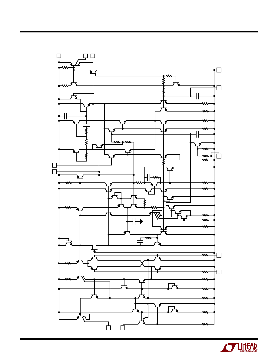
SCHE ATIC DIAGRA
W
W
15
LT1020
sn1020 1020fcs
U
PACKAGE DESCRIPTIO
J Package
14-Lead CERDIP (Narrow .300 Inch, Hermetic)
(Reference LTC DWG # 05-08-1110)
N Package
14-Lead PDIP (Narrow .300 Inch)
(Reference LTC DWG # 05-08-1510)
J14 0801
.045 ≠ .065
(1.143 ≠ 1.651)
.100
(2.54)
BSC
.014 ≠ .026
(0.360 ≠ 0.660)
.200
(5.080)
MAX
.015 ≠ .060
(0.381 ≠ 1.524)
.125
(3.175)
MIN
.300 BSC
(7.62 BSC)
.008 ≠ .018
(0.203 ≠ 0.457)
0
∞
≠ 15
∞
1
2
3
4
5
6
7
.220 ≠ .310
(5.588 ≠ 7.874)
.785
(19.939)
MAX
.005
(0.127)
MIN
14
11
8
9
10
13
12
.025
(0.635)
RAD TYP
NOTE: LEAD DIMENSIONS APPLY TO SOLDER DIP/PLATE
OR TIN PLATE LEADS
N14 1002
.020
(0.508)
MIN
.120
(3.048)
MIN
.130
±
.005
(3.302
±
0.127)
.045 ≠ .065
(1.143 ≠ 1.651)
.065
(1.651)
TYP
.018
±
.003
(0.457
±
0.076)
.005
(0.125)
MIN
.255
±
.015*
(6.477
±
0.381)
.770*
(19.558)
MAX
3
1
2
4
5
6
7
8
9
10
11
12
13
14
.008 ≠ .015
(0.203 ≠ 0.381)
.300 ≠ .325
(7.620 ≠ 8.255)
.325
+.035
≠.015
+0.889
≠0.381
8.255
(
)
NOTE:
1. DIMENSIONS ARE
INCHES
MILLIMETERS
*THESE DIMENSIONS DO NOT INCLUDE MOLD FLASH OR PROTRUSIONS.
MOLD FLASH OR PROTRUSIONS SHALL NOT EXCEED .010 INCH (0.254mm)
.100
(2.54)
BSC
OBSOLETE PACKAGE
Information furnished by Linear Technology Corporation is believed to be accurate and reliable.
However, no responsibility is assumed for its use. Linear Technology Corporation makes no represen-
tation that the interconnection of its circuits as described herein will not infringe on existing patent rights.
16
LT1020
sn1020 1020fcs
©
LINEAR TECHNOLOGY CORPORATION 1993
LT/TP 0203 1K REV C ∑ PRINTED IN USA
U
PACKAGE DESCRIPTIO
SW Package
16-Lead Plastic Small Outline (Wide .300 Inch)
(Reference LTC DWG # 05-08-1620)
Linear Technology Corporation
1630 McCarthy Blvd., Milpitas, CA 95035-7417
(408) 432-1900
q
FAX: (408) 434-0507
q
www.linear.com
S16 (WIDE) 0502
NOTE 3
.398 ≠ .413
(10.109 ≠ 10.490)
NOTE 4
16
15
14
13
12
11
10
9
1
N
2
3
4
5
6
7
8
N/2
.394 ≠ .419
(10.007 ≠ 10.643)
.037 ≠ .045
(0.940 ≠ 1.143)
.004 ≠ .012
(0.102 ≠ 0.305)
.093 ≠ .104
(2.362 ≠ 2.642)
.050
(1.270)
BSC
.014 ≠ .019
(0.356 ≠ 0.482)
TYP
0
∞
≠ 8
∞
TYP
NOTE 3
.009 ≠ .013
(0.229 ≠ 0.330)
.005
(0.127)
RAD MIN
.016 ≠ .050
(0.406 ≠ 1.270)
.291 ≠ .299
(7.391 ≠ 7.595)
NOTE 4
◊
45
∞
.010 ≠ .029
(0.254 ≠ 0.737)
INCHES
(MILLIMETERS)
NOTE:
1. DIMENSIONS IN
2. DRAWING NOT TO SCALE
3. PIN 1 IDENT, NOTCH ON TOP AND CAVITIES ON THE BOTTOM OF PACKAGES ARE THE MANUFACTURING OPTIONS.
THE PART MAY BE SUPPLIED WITH OR WITHOUT ANY OF THE OPTIONS
4. THESE DIMENSIONS DO NOT INCLUDE MOLD FLASH OR PROTRUSIONS.
MOLD FLASH OR PROTRUSIONS SHALL NOT EXCEED .006" (0.15mm)
.420
MIN
.325
±
.005
RECOMMENDED SOLDER PAD LAYOUT
.045
±
.005
N
1
2
3
N/2
.050 BSC
.030
±
.005
TYP
RELATED PARTS
PART NUMBER
DESCRIPTION
COMMENTS
LT1120/LT1120A
125mA, Micropower Regulator and Comparators
V
IN
: 4.5V to 36V; V
OUT(MIN)
: 2.50V, Dropout Voltage (V at I
OUT
): 0.40V;
I
Q
(Supply): 40
µ
A; V
OUT
(V): Adj; I
SD
: 10
µ
A; S8, N8; Comparator and
Reference, Logic Shutdown, Ref Sources and Sinks 2/4mA
LT1121/LT1121HV 150mA, Micropower, LDO
V
IN
: 4.2V to 30/36V; V
OUT(MIN)
: 3.75V, Dropout Voltage (V at I
OUT
): 0.42V;
I
Q
(Supply): 30
µ
A; V
OUT
(V): Adj, 3.3, 5; I
SD
: 16
µ
A; SOT-223, S8, Z;
Reverse-Battery Protection
LT1129
700mA, Micropower, LDO
V
IN
: 4.2V to 30V; V
OUT(MIN)
: 3.75V, Dropout Voltage (V at I
OUT
): 0.40V;
I
Q
(Supply): 50
µ
A; V
OUT
(V): Adj, 3.3, 5; I
SD
: 16
µ
A; DD, SOT-223, S8,
TO220-5, TSSOP20
LT1616
25V, 500mA (I
OUT
), 1.4MHz, High Efficiency
V
IN
: 3.6V to 25V, V
OUT(MIN)
: 1.25V, I
Q
: 1.9mA, I
SD
: <1
µ
A, ThinSOT
Step-Down DC/DC Converter
LT1676
60V, 440mA (I
OUT
), 100kHz, High Efficiency
V
IN
: 7.4V to 60V, V
OUT(MIN)
: 1.24V, I
Q
: 3.2mA, I
SD
: 2.5
µ
A, S8
Step-Down DC/DC Converter
LT1761
100mA, Low Noise Micropower, LDO
V
IN
: 1.8V to 20V; V
OUT(MIN)
: 1.22V, Dropout Voltage (V at I
OUT
): 0.30V;
I
Q
(Supply): 20
µ
A; V
OUT
(V): Adj, 1.5, 1.8, 2, 2.5, 2.8, 3, 3.5, 5; I
SD
: <1
µ
A;
ThinSOT; Low Noise < 20
µ
V
RMSP-P
, Stable with 1
µ
F Ceramic Capacitors