 | –≠–ª–µ–∫—Ç—Ä–æ–Ω–Ω—ã–π –∫–æ–º–ø–æ–Ω–µ–Ω—Ç: LT1022AM | –°–∫–∞—á–∞—Ç—å:  PDF PDF  ZIP ZIP |
1
LT1022
1022fa
Guaranteed
Slew Rate: 23V/µs Min
Guaranteed
Offset Voltage: 250µV Max
≠ 55∞C to 125∞C: 750µV Max
Guaranteed
Drift: 5µV/∞C Max
Guaranteed
Bias Current:
70∞C, 180pA Max
125∞C, 4nA Max
Gain-Bandwidth Product: 8.5MHz Typ
Settling Time to 0.05% (10V Step): 0.9µs Typ
The LT
Æ
1022 JFET input operational amplifier combines
high speed and precision performance.
A 26V/µs slew rate and 8.5MHz gain-bandwidth product
are simultaneously achieved with offset voltage of
typically 80µV, 1.5µV/∞C drift, bias currents of 50pA at
70∞C, 500pA at 125∞C. The output delivers 20mA of load
current without gain degradation.
The 250µV maximum offset voltage specification
represents less than 1/2 least significant bit error in a
14-bit, 10V system.
The LT1022A meets or exceeds all OP-16A and OP-16E
specifications. It is faster and more accurate without
stability problems at cold temperatures.
The LT1022 can be used as the output amplifier for 12-bit
current output D/A converters, as shown below.
For a more accurate, lower power dissipation, but slower
JFET input op amp, please refer to the LT1055 data sheet.
Fast D/A Output Amplifiers (12, 14, 16 Bits)
High Speed Instrumentation
Fast, Precision Sample and Hold
Voltage-to-Frequency Converters
Logarithmic Amplifiers
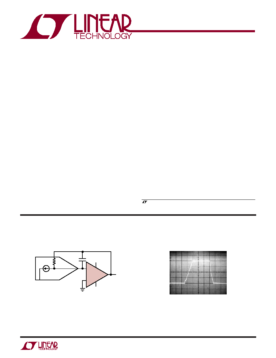
12-Bit Voltage Output D/A Converter
High Speed, Precision
JFET Input Operational Amplifier
Large-Signal Response
FEATURES
DESCRIPTIO
U
APPLICATIO S
U
C
F
= 15pF TO 33pF
SETTLING TIME TO 2mV (0.8 LSB) = 1.5µs TO 2µs
LT1022 ∑ TA01
≠
+
LT1022
≠15V
15V
12-BIT CURRENT OUTPUT D/A
CONVERTER (e.g., 6012, 565 OR DAC-80)
0mA TO 2mA
OR 4mA
2
3
7
6
4
OUTPUT
0V TO 10V
C
F
0.5µs/DIV
5V/DIV
, LTC and LT are registered trademarks of Linear Technology Corporation.
TYPICAL APPLICATIO
U
A
V
= 1
C
L
= 100pF
T
A
= 25∞C
V
S
= ±15V

2
LT1022
1022fa
LT1022AMH
LT1022MH
LT1022ACH
LT1022CH
ORDER PART
NUMBER
TOP VIEW
N/C
≠IN
OUT
V+
+IN
BALANCE
BALANCE
V ≠
METAL CAN H PACKAGE
T
JMAX
= 150
∞
C,
JA
= 150
∞
C/W,
JC
= 45
∞
C/W
8
4
7
1
5
3
6
2
ORDER PART
NUMBER
LT1022CN8
LT1022 ∑ POI01
TOP VIEW
N8 PACKAGE 8-LEAD PDIP
T
JMAX
= 100
∞
C,
JA
= 130
∞
C/W
1
2
3
4
8
7
6
5
BAL
≠IN
+IN
V ≠
N/C
V+
OUT
BAL
OBSOLETE PACKAGE
Consider the N8 Package as an Alternate Source
LT1022AM
LT1022M, LT1022CH
LT1022AC
LT1022CN8
SYMBOL
PARAMETER
CONDITIONS
MIN
TYP
MAX
MIN
TYP
MAX
UNITS
V
OS
Input Offset Voltage (Note 2)
H Package
80
250
100
600
µV
N8 Package
160
1000
µV
l
OS
Input Offset Current
Fully Warmed Up
2
10
2
20
pA
I
B
Input Bias Current
Fully Warmed Up
±10
±50
±10
±50
pA
V
CM
= + 10V
30
100
30
150
pA
Input Resistance--Differential
10
12
10
12
--Common Mode
V
CM
= ≠11V to 8V
10
12
10
12
V
CM
= 8V to 11V
10
11
10
11
Input Capacitance
4
4
pF
e
n
Input Noise Voltage
0.1Hz to 10Hz
2.5
2.8
µV/
P-P
e
n
Input Noise Voltage Density
f
O
= 10Hz (Note 3)
28
50
30
60
nV/Hz
f
O
= 1kHz (Note 4)
14
20
15
22
nV/Hz
i
n
Input Noise Current Density
f
O
= 10Hz, 1kHz (Note 5)
1.8
4
1.8
4
fAHz
A
VOL
Large Signal Voltage Gain
V
O
= ±10V R
L
= 2k
150
400
120
400
V/mV
R
L
= 1k
130
300
100
300
V/mV
Input Voltage Range
±10.5
±12
±10.5
±12
V
CMRR
Common-Mode Rejection Ratio
V
CM
= ±10.5V
86
94
82
92
dB
PSRR
Power Supply Rejection Ratio
V
S
= ±10V to ±18V
88
104
86
102
dB
V
OUT
Output Voltage Swing
R
L
= 2k
±12
±13.2
±12
±13.2
V
SR
Slew Rate
23
26
18
24
V/µs
Supply Voltage ...................................................... ±20V
Differential Input Voltage ....................................... ±40V
Input Voltage ......................................................... ±20V
Output Short Circuit Duration .......................... Indefinite
PACKAGE/ORDER I FOR ATIO
U
U
W
ABSOLUTE AXI U RATI GS
W
W
W
U
ELECTRICAL CHARACTERISTICS
(Note 1)
V
S
= ± 15V, T
A
= 25∞C, V
CM
= 0V unless otherwise noted.
Consult LTC Marketing for parts specified with wider operating temperature ranges.
Operating Temperature Range
LT1022AM/1022M (OBSOLETE).........≠ 55∞C to 125∞C
LT1022AC/1022C .................................... 0∞C to 70∞C
Storage Temperature Range .................. ≠65∞C to 150∞C
Lead Temperature (Soldering, 10 sec.)................. 300∞C

3
LT1022
1022fa
ELECTRICAL CHARACTERISTICS
The
denotes the specifications which apply over the full operating temperature range of V
CM
= 0V, 0∞C T
A
70∞C. V
S
= ± 15V,
unless otherwise noted.
LT1022CH
LT1022AC
LT1022CN8
SYMBOL
PARAMETER
CONDITIONS
MIN
TYP
MAX
MIN
TYP
MAX
UNITS
V
OS
Input Offset Voltage
H Package
140
480
180
1000
µV
(Note 2)
N8 Package
300
1700
µV
Average Temperature
H Package
1.3
5.0
1.8
9.0
µV/∞C
Coefficient of Input Offset Voltage
N8 Package (Note 6)
3.0
15.0
µV/∞C
I
OS
Input Offset Current
Warmed Up, T
A
= 70∞C
15
80
18
100
pA
I
B
Input Bias Current
Warmed Up, T
A
= 70∞C
±50
±200
±60
±250
pA
A
VOL
Large-Signal Voltage Gain
V
O
= ±10V, R
L
= 2k
80
250
60
250
V/mV
CMRR
Common Mode Rejection Ratio
V
CM
= ±10.4V
85
93
80
91
dB
PSRR
Power Supply Rejection Ratio
V
S
= ±10V to ±18V
86
103
84
101
dB
V
OUT
Output Voltage Swing
R
L
= 2k
±12
±13.1
±12
±13.1
V
LT1022AM
LT1022M
SYMBOL
PARAMETER
CONDITIONS
MIN
TYP
MAX
MIN
TYP
MAX
UNITS
V
OS
Input Offset Voltage
(Note 2)
230
750
300
1500
µV
Average Temperature
(Note 6)
1.5
5.0
2.0
9.0
µV/∞C
Coefficient of Input Offset Voltage
I
OS
Input Offset Current
Warmed Up, T
A
= 125∞C
0.3
2.0
0.30
3.0
nA
I
B
Input Bias Current
Warmed Up, T
A
= 125∞C
± 0.5
± 4.0
± 0.7
± 6.0
nA
A
VOL
Large Signal Voltage Gain
V
O
= ±10V, R
L
= 2k
40
120
35
120
V/mV
CMRR
Common-Mode Rejection Ratio
V
CM
= ±10.4V
85
92
80
90
dB
PSRR
Power Supply Rejection Ratio
V
S
= ±10V to ±17V
86
102
84
100
dB
V
OUT
Output Voltage Swing
R
L
= 2k
±12
±12.9
±12
±12.9
V
Note 1: Absolute Maximum Ratings are those values beyond which the
life of a device may be impaired.
Note 2: Offset voltage is measured under two different conditions:
(a) approximately 0.5 seconds after application of power;
(b) at T
A
= 25∞C, with the chip self-heated to approximately 45∞C
to account for chip temperature rise when the device is fully warmed up.
Note 3: 10Hz noise voltage density is sample tested on every lot of A
grades. Devices 100% tested at 10Hz are available on request.
Note 4: This parameter is tested on a sample basis only.
Note 5: Current noise is calculated from the formula: i
n
= (2qI
B
)
1/2
, where
q = 1.6 ∑ 10
≠19
coulomb. The noise of source resistors up to 1G swamps
the contribution of current noise.
Note 6: Offset voltage drift with temperature is practically unchanged when
the offset voltage is trimmed to zero with a 100k potentiometer between
the balance terminals and the wiper tied to V
+
. Devices tested to tighter
drift specifications are available on request.
The
denotes the specifications which apply over the full operating temperature range of ≠ 55∞C T
A
125∞C. V
S
= ±15V, V
CM
= 0V,
unless otherwise noted.
LT1022AM
LT1022M, LT1022CH
LT1022AC
LT1022CN8
SYMBOL
PARAMETER
CONDITIONS
MIN
TYP
MAX
MIN
TYP
MAX
UNITS
GBW
Gain-Bandwidth Product
f = 1MHz
8.5
8.0
MHz
I
S
Supply Current
5.2
7.0
5.2
7.0
mA
Settling Time
A = +1 or A = ≠1
10V Step to 0.05%
0.9
0.9
µs
10V Step to 0.02%
1.3
1.3
µs
Offset Voltage Adjustment Range
R
POT
= 100k
±7
±7
mV
V
S
= ± 15V, T
A
= 25∞C, V
CM
= 0V unless otherwise noted.

4
LT1022
1022fa
Undistorted Output Swing vs
Frequency
Gain vs Frequency
Small-Signal Response
Phase Margin, Gain Bandwidth
Product, Slew Rate vs Temperature
Settling Time
Gain, Phase Shift vs Frequency
The typical behavior of many LT1022 parameters is identical to the LT1056. Please refer to the LT1055/1056 data
sheet for the following typical performance characteristics:
Input Bias and Offset Currents vs Temperature
Short Circuit Current vs Time
Input Bias Current Over the Common-Mode Range
Output Impedance vs Frequency
Distribution of Input Offset Voltage (H and N8 Package)
Common Mode Range vs Temperature
Distribution of Offset Voltage Drift with Temperature
Common Mode and Power Supply Rejections vs Temperature
Warm-Up Drift
Common Mode Rejection Ratio vs Frequency
Long Term Drift of Representative Units
Power Supply Rejection Ratio vs Frequency
0.1Hz to 10Hz Noise
Voltage Gain vs Temperature
Voltage Noise vs Frequency
Supply Current vs Supply Voltage
Noise vs Chip Temperature
Output Swing vs Load Resistance
TYPICAL PERFOR A CE CHARACTERISTICS
U
W
FREQUENCY (Hz)
1
GAIN (dB)
60
100
100M
LT1022 ∑ TPC01
20
≠20
100
10k
1M
10
1k
100k
10M
140
40
80
0
120
V
S
= ±15V
T
A
= ≠55∞C
T
A
= 125∞C
T
A
= 25∞C
FREQUENCY (MHz)
1
≠10
GAIN (dB)
PHASE SHIFT (DEGREES)
0
10
30
10
100
3
30
LT1022 ∑ TPC02
20
240
200
160
80
120
220
180
140
100
C
LMAX
500pF
(A
V
= +1)
C
L
= 10pF
C
L
= 300pF
C
L
= 300pF
C
L
= 10pF
PHASE
GAIN
V
S
= ±15V
T
A
= 25∞C
FREQUENCY (Hz)
100k
0
PEAK-TO-PEAK OUTPUT SWING (V)
6
12
18
24
1M
10M
LT1022 ∑ TPC04
30
V
S
= ±15V
T
A
= 25∞C
SETTLING TIME (µs)
0
OUTPUT VOLTAGE SWING FROM 0V (V)
0
LT1022 ∑ TPC05
≠5
≠10
1
2
5
10
3
V
S
= ±15V
T
A
= 25∞C
10mV
5mV
5mV
2mV
2mV
1mV
10mV
1mV
0.5mV
0.5mV
0.2µs/DIV
20mV/DIV
A
V
= +1
C
L
= 100pF
T
A
= 25∞C
V
S
= ±15V
TEMPERATURE (
∞
C)
≠50
40
PHASE MARGIN (DEGREES)
SLEW RATE (V/
µ
s)
GAIN BANDWIDTH PRODUCT (MHz)
60
40
0
50
75
LT1022 ∑ TPC03
50
30
20
10
11
12
7
6
8
9
≠25
25
100
125
V
S
=
±
15V
C
L
= 10pF
M
SLEW
GBW (f = 1MHz)

5
LT1022
1022fa
Fast Piezoelectric Accelerometer
APPLICATIO S I FOR ATIO
W
U
U
U
The LT1056 applications information is directly
applicable to the LT1022. Please consult the
LT1055/1056 data sheet for details on:
(1) plug-in compatibility to industry standard devices
(2) offset nulling
(3) achieving picoampere/microvolt performance
(4) phase-reversal protection
(5) high speed operation (including settling time
test circuit)
(6) noise performance
(7) simplified circuit schematic
TYPICAL APPLICATIO S
U
1pF TO 5pF
OUTPUT
2
3
6
7
4
LT1022 ∑ TA03
≠
+
LT1022
10
10
15V
≠15V
ENDEVCO #2215
ACCELEROMETER

6
LT1022
1022fa
10Hz to 1MHz Voltage-to-Frequency Converter
2
3
7
8
4
1
≠15V
15V
5k
1.8k
1.8k
LT1009
LT1022 ∑ TA04
≠
+
≠
+
≠
+
LT1011
LT1022
LT1011
1k
1k
INPUT
0V TO 10V
15V
1.8k
1000pF
2N2222
2N2222
2N2222
15V
15V
1.8k
1.8k
20k
1.8k
10k
4.7k
TTL OUTPUT
15V
15V
≠15V
≠15V
≠15V
100pF
(POLYSTYRENE)
100k
10pF
1
2
3
7
8
2
4
6
7
3
4
0.1µF
200k
100k
22.1k
(METAL FILM)
= 1N4148
TYPICAL APPLICATIO S
U

7
LT1022
1022fa
2
3
7
8
4
1
≠15V
15V
1.8k
1.8k
LT1004
2.5V
LT1022 ∑ TA05
≠
+
≠
+
≠
+
LT1011
LT1022
LT1011
1k
1k
LM329
15V
1.8k
1000pF
2N2222
2N2222
2N2222
15V
15V
1.8k
1.8k
20k
1.8k
10k
4.7k
15V
15V
≠15V
≠15V
≠15V
≠15V
5pF
FULL-SCALE TRIM
100k
2pF
2
3
7
8
2
4
6
7
3
4
1
0.1
µ
F
200k
100k
4.7k
10M
LIGHT
INPUT
= 1N4148
= HEWLETT PACKARD PHOTODIODE HP5082-4204
SCALE FACTOR =
1nW/Hz AT 900 NANOMETERS FROM 20nW TO 2mW
POLYSTYRENE
* SELECT VALUE FOR 2mW IN = 2MHz OUT
3.3M
10k
DARK
CURRENT
TRIM
47pF*
TTL OUTPUT
20Hz 2MHz
PIN Photodiode-to-Frequency Converter
TYPICAL APPLICATIO S
U

8
LT1022
1022fa
TYPICAL APPLICATIO S
U
Fast, Differential Input Current Source
LT1022 ∑ TA07
6
10pF
15V
≠15V
3
2
7
4
LT1022
+
≠
V
IN1
R
L
I
OUT
I
OUT
=
V
IN2
≠ V
IN1
V
IN2
R*
R*
R*
R*
R
2
I
OUTP-P ∑
R
L
*MATCH TO 0.01%
FULL-SCALE POWER BANDWIDTH
= 1MHz FOR I
OUT
R = 8V
P-P
= 400kHz FOR I
OUT
R = 20V
P-P
MAXIMUM I
OUT
= 10mA
P-P
COMMON-MODE VOLTAGE AT LT1022 INPUT =
Wide Bandwidth Absolute Value Circuit
LT1022 ∑ TA06
3
2
3
2
7
6
7
6
4
LT1022
+
≠
4
LT1022
+
≠
10k*
10k*
10k*
10pF
10pF
10k*
10k*
INPUT
±10V
1N4148
1N4148
15V
15V
≠15V
≠15V
OUTPUT
0V TO 10V
*0.1%
1% ACCURACY TO 300kHz
5% ACCURACY TO 700kHz

9
LT1022
1022fa
TYPICAL APPLICATIO S
U
Low Distortion Sine Wave Oscillator
LT1022 ∑ TA09
6
15V
≠15V
3
2
7
4
≠
LT1022
953
*
10k
10k
953
*
430
+
≠
0.033
µ
F
0.033
µ
F
OUTPUT
1% FILM
10k DUAL POTENTIOMETER --
MATCH TRACKING TO 0.1%
MATCH CAPACITORS TO 0.1%
5kHz TO 50kHz RANGE
DISTORTION < 0.1%
AMPLITUDE = 18V
P-P
# 327 LAMP
*
High Output Current Op Amp
15V
≠15V
LT1022 ∑ TA08
6
C
F
15V
≠15V
3
2
10k
OUTPUT
SLEW RATE = 26V/µs
I
OUT
= 150mA
C
L
CAN BE 1µF
A
V
= +1, C
F
= 1000pF
A
V
= ≠1, C
F
= 10pF
7
4
LT1022
LT1010
+
≠
R
S

10
LT1022
1022fa
TYPICAL APPLICATIO S
U
LT1020 ∑ TA10
LT1022
LT1010
1000pF
POLYSTYRENE
OUTPUT
10k
3.5k
2N2222
13k
15pF
2N2369
2N2907
1.5k
20k
3k
LT1022
LT318A
820
820
0.1
µ
F
4.7k*
INPUT
330pF
15V
TTL
INPUT
5k
HOLD STEP
COMPENSATION
TRIM
16ns APERTURE TIME
2
µ
s ACQUISITION TIME TO 0.01%
SAMPLE-AND-HOLD OFFSET < 250
µ
V
HOLD SETTLING < 100ns
≠15V
≠15V
1k
39pF
HP5082-2810
1N4148
2k
LEVEL SHIFT
1k
SAMPLE-AND-HOLD
SIGNAL PATH
2N4393
470
1000pF
HOLD STEP
COMPENSATION
20pF
5.1k
HP5082-2810
≠
+
≠
+
≠
+
2N2369
2N2222
1N4148
Fast, Precision Sample-And-Hold

11
LT1022
1022fa
Information furnished by Linear Technology Corporation is believed to be accurate and reliable.
However, no responsibility is assumed for its use. Linear Technology Corporation makes no represen-
tation that the interconnection of its circuits as described herein will not infringe on existing patent rights.
U
PACKAGE DESCRIPTIO
H Package
8-Lead TO-5 Metal Can (.200 Inch PCD)
(Reference LTC DWG # 05-08-1320)
0.050
(1.270)
MAX
0.016 ≠ 0.021**
(0.406 ≠ 0.533)
0.010 ≠ 0.045*
(0.254 ≠ 1.143)
SEATING
PLANE
0.040
(1.016)
MAX
0.165 ≠ 0.185
(4.191 ≠ 4.699)
GAUGE
PLANE
REFERENCE
PLANE
0.500 ≠ 0.750
(12.700 ≠ 19.050)
0.305 ≠ 0.335
(7.747 ≠ 8.509)
0.335 ≠ 0.370
(8.509 ≠ 9.398)
DIA
0.200
(5.080)
TYP
0.027 ≠ 0.045
(0.686 ≠ 1.143)
0.028 ≠ 0.034
(0.711 ≠ 0.864)
0.110 ≠ 0.160
(2.794 ≠ 4.064)
INSULATING
STANDOFF
45∞TYP
H8(TO-5) 0.200 PCD 1197
LEAD DIAMETER IS UNCONTROLLED BETWEEN THE REFERENCE PLANE
AND 0.045" BELOW THE REFERENCE PLANE
FOR SOLDER DIP LEAD FINISH, LEAD DIAMETER IS
0.016 ≠ 0.024
(0.406 ≠ 0.610)
*
**
PIN 1
OBSOLETE PACKAGE

12
LT1022
1022fa
Linear Technology Corporation
1630 McCarthy Blvd., Milpitas, CA 95035-7417
(408) 432-1900
FAX: (408) 434-0507
www.linear.com
LW/TP 0902 1K REV A ∑ PRINTED IN USA
LINEAR TECHNOLOGY CORPORATION 1985
N8 1098
0.100
(2.54)
BSC
0.065
(1.651)
TYP
0.045 ≠ 0.065
(1.143 ≠ 1.651)
0.130 ± 0.005
(3.302 ± 0.127)
0.020
(0.508)
MIN
0.018 ± 0.003
(0.457 ± 0.076)
0.125
(3.175)
MIN
1
2
3
4
8
7
6
5
0.255 ± 0.015*
(6.477 ± 0.381)
0.400*
(10.160)
MAX
0.009 ≠ 0.015
(0.229 ≠ 0.381)
0.300 ≠ 0.325
(7.620 ≠ 8.255)
0.325
+0.035
≠0.015
+0.889
≠0.381
8.255
(
)
*THESE DIMENSIONS DO NOT INCLUDE MOLD FLASH OR PROTRUSIONS.
MOLD FLASH OR PROTRUSIONS SHALL NOT EXCEED 0.010 INCH (0.254mm)
N8 Package
8-Lead PDIP (Narrow .300 Inch)
(Reference LTC DWG # 05-08-1510)
U
PACKAGE DESCRIPTIO