 | –≠–ª–µ–∫—Ç—Ä–æ–Ω–Ω—ã–π –∫–æ–º–ø–æ–Ω–µ–Ω—Ç: LT1025A | –°–∫–∞—á–∞—Ç—å:  PDF PDF  ZIP ZIP |
1
LT1025
1025fa
DESCRIPTIO
U
APPLICATIO S
U
s
80
µ
A Supply Current
s
4V to 36V Operation
s
0.5
∞
C Initial Accuracy (A Version)
s
Compatible with Standard Thermocouples
(E, J, K, R, S, T)
s
Auxiliary 10mV/
∞
C Output
s
Thermocouple Cold Junction Compensator
s
Centigrade Thermometer
s
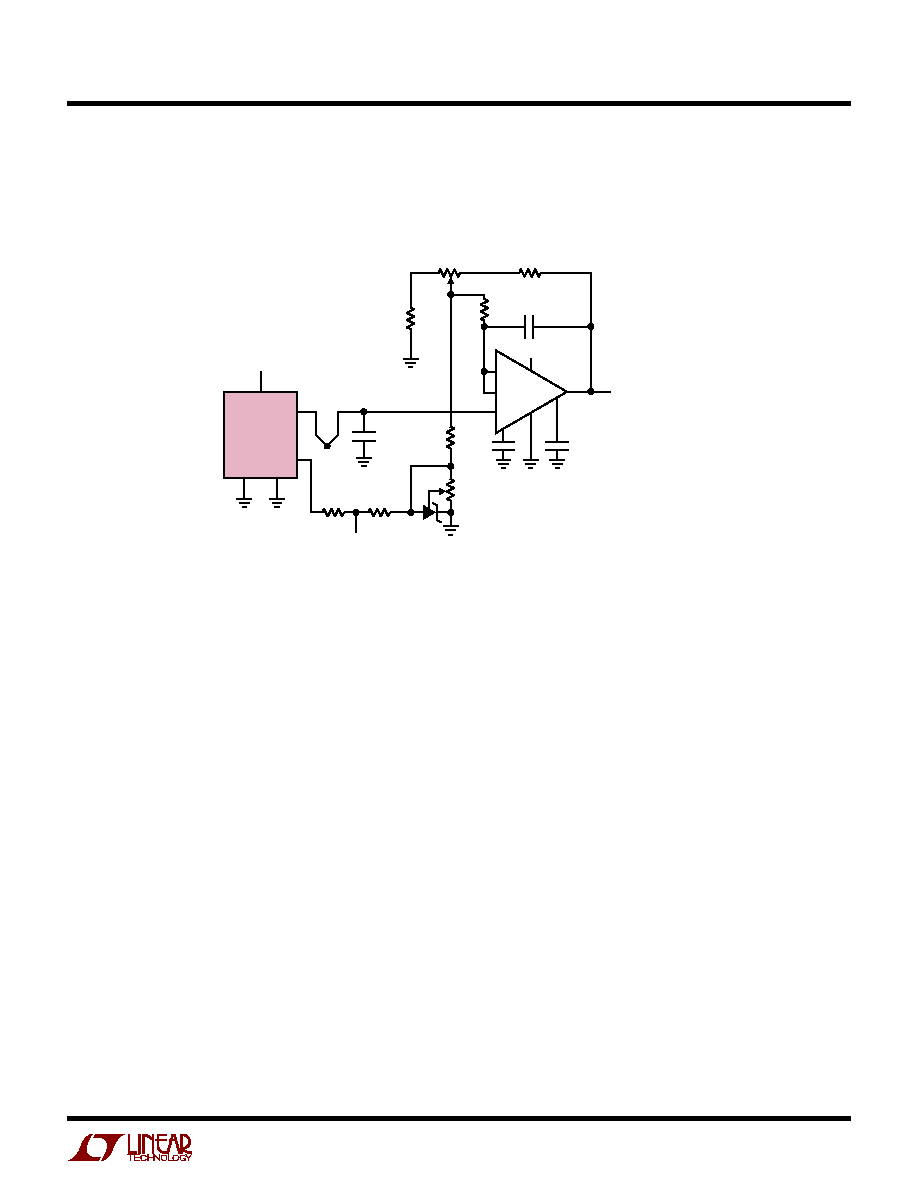
Temperature Compensation Network
Micropower Thermocouple
Cold Junction Compensator
Type K 10mV/
∞
C Thermometer
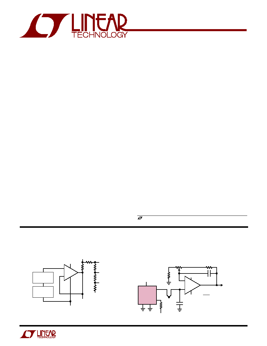
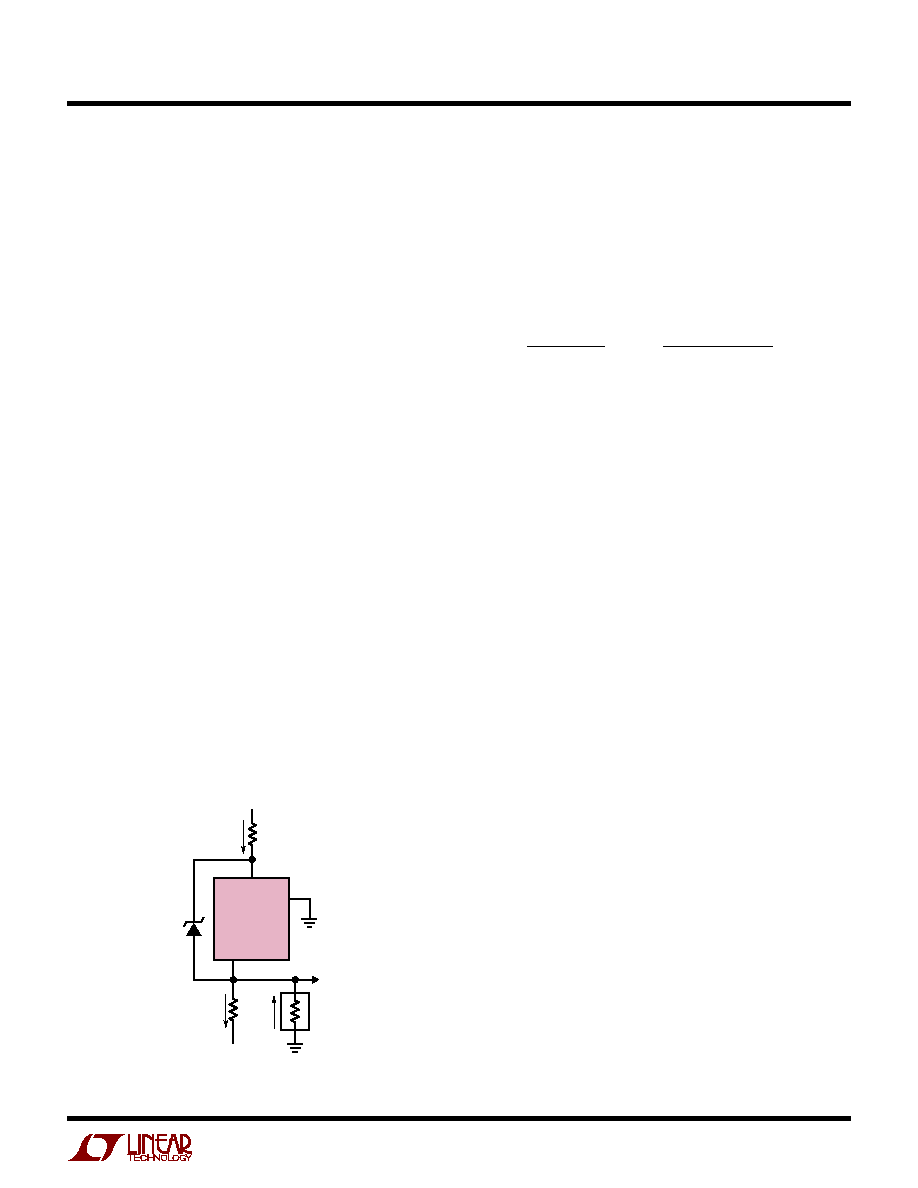
The LT
Æ
1025 is a micropower thermocouple cold junction
compensator for use with type E, J, K, R, S, and T
thermocouples. It utilizes wafer level and post-package
trimming to achieve 0.5
∞
C initial accuracy. Special curvature
correction circuitry is used to match the "bow" found in all
thermocouples so that accurate cold junction compensation
is maintained over a wider temperature range.
The LT1025 will operate with a supply voltage from 4V to 36V.
Typical supply current is 80
µ
A, resulting in less than 0.1
∞
C
internal temperature rise for supply voltages under 10V.
A 10mV/
∞
C output is available at low impedance, in addition
to the direct thermocouple voltages of 60.9
µ
V/
∞
C (E),
51.7
µ
V/
∞
C (J), 40.3
µ
V/
∞
C (K, T) and 5.95
µ
V/
∞
C (R, S). All
outputs are essentially independent of power supply voltage.
A special kit is available (LTK001) which contains an LT1025
and a custom tailored thermocouple amplifier. The amplifier
and compensator are matched to allow a much tighter specifi-
cation of temperature error than would be obtained by adding
the compensator and amplifier errors on a worst-case basis.
The amplifier from this kit is available separately as LTKA0x.
The LT1025 is available in an 8-pin PDIP for temperatures
between 0
∞
C and 70
∞
C.
≠
≠
+
BOW*
CORRECTION
VOLTAGE
BUFFER
V
IN
GND
E 60.9
µ
V/
∞
C
V
0
10mV/
∞
C
R≠ COMMON
J 51.7
µ
V/
∞
C
K,T 40.6
µ
V/
∞
C
R, S 6
µ
V/
∞
C
10mV/
∞
C
TEMPERATURE
SENSOR
*CORRECTS FOR BOW
IN
COLD JUNCTION,
NOT
IN PROBE (HOT JUNCTION)
LT1025 ∑ BD01
+
≠
LTKA0x
TYPE K
R4*
V
+
V
+
R1
1k
1%
C2
0.1
µ
F
C1
0.1
µ
F
≠
+
R2
100
FULL-SCALE TRIM
V
OUT
10mV/
∞
C
R3**
255k
1%
V
≠
V
≠
30
µ
A
V
≠
GND R
≠
V
O
K
LT1025
*R4
, R4 IS NOT REQUIRED
(OPEN) FOR LT1025 TEMPERATURES
0
∞
C
**SELECTED FOR 0
∞
C TO 100
∞
C RANGE
OR EQUIVALENT. SEE
"AMPLIFIER CONSIDERATIONS"
V
IN
LT1025 ∑ TA01
FEATURES
, LTC and LT are registered trademarks of Linear Technology Corporation.
BLOCK DIAGRA
W
TYPICAL APPLICATIO
U
2
LT1025
1025fa
PARAMETER
CONDITIONS
MIN
TYP
MAX
UNITS
Temperature Error at
T
J
= 25
∞
C
10mV/
∞
C Output (Notes 4, 5)
LT1025A
0.3
0.5
∞
C
LT1025
0.5
2.0
∞
C
Full Temperature Span
q
See Curve
Resistor Divider Accuracy
V
OUT
= 10mV/
∞
C
(Notes 2, 4)
LT1025A
E
60.6
60.9
61.3
µ
V/
∞
C
J
51.4
51.7
52.1
µ
V/
∞
C
K, T
40.3
40.6
41.0
µ
V/
∞
C
R, S
5.8
5.95
6.2
µ
V/
∞
C
LT1025
E
60.4
60.9
61.6
µ
V/
∞
C
J
51.2
51.7
52.3
µ
V/
∞
C
K, T
40.2
40.6
41.2
µ
V/
∞
C
R, S
5.75
5.95
6.3
µ
V/
∞
C
Supply Current
4V
V
IN
36V
50
80
100
µ
A
LT1025AC, LT1025C
q
50
150
µ
A
LT1025AM, LT1025M
q
200
µ
A
Line Regulation (Note 3)
4V
V
IN
36V
q
0.003
0.02
∞
C/V
Load Regulation (Note 3)
0
I
O
1mA
q
0.04
0.2
∞
C
Divider Impedance
E
2.5
k
J
2.1
k
K, T
4.4
k
R, S
3.8
k
Change in Supply Current
4V
V
IN
36V
0.01
0.05
µ
A/V
(Note 1)
Input Supply Voltage .......................................... 36V
Output Voltage (Forced) ........................................ 5V
Output Short-Circuit Duration ..................... Indefinite
Operating Temperature Range
LT1025AC, LT1025C ............................ 0
∞
C to 70
∞
C
LT1025AM, LT1025M .................. ≠ 55
∞
C to 125
∞
C
Storage Temperature Range ............ ≠ 55
∞
C to 150
∞
C
The
q
denotes the specifications which apply over the full operating
temperature range, otherwise specificatons are at T
A
= 25
∞
C. V
S
= 5V, Pin 5 tied to Pin 4, unless otherwise noted.
Note 1: Absolute Maximum Ratings are those values beyond which the
life of a device may be impaired.
Note 2: Divider accuracy is measured by applying a 10.000V signal to the
output divider and measuring the individual outputs.
Note 3: Regulation does not include the effects of self-heating. See
"Internal Temperature Rise" in Application Guide. Load regulation is
30
µ
A
I
O
1mA for T
A
0
∞
C.
ABSOLUTE AXI U RATI GS
W
W
W
U
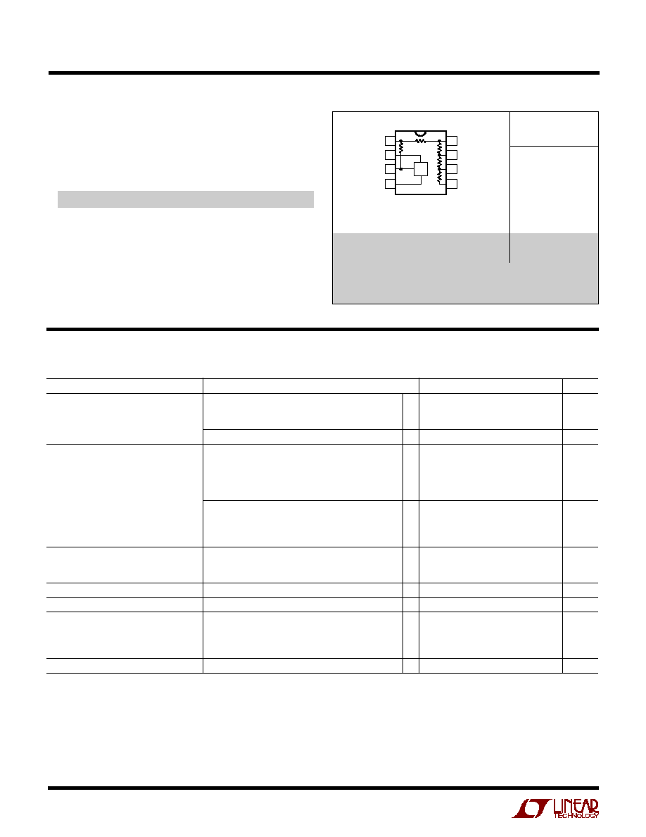
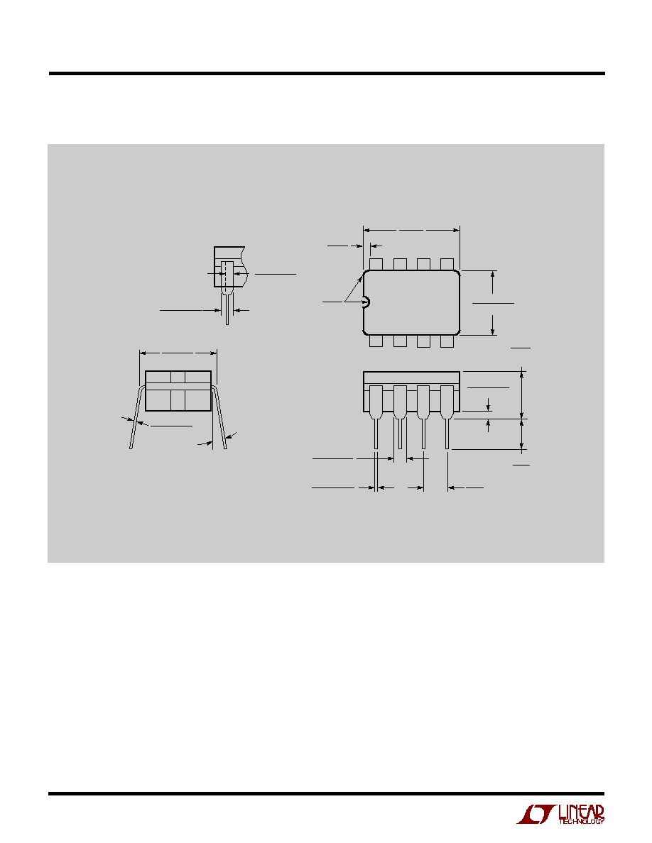
PACKAGE/ORDER I FOR ATIO
U
U
W
ELECTRICAL CHARACTERISTICS
Note 4: To calculate total temperature error at individual thermocouple
outputs, add 10mV/
∞
C output error to the resistor divider error. Total error
for type K output at 25
∞
C with an LT1025A is 0.5
∞
C plus (0.4
µ
V/
∞
C)(25
∞
C)/
(40.6
µ
V/
∞
C) = 0.5
∞
C + 0.25
∞
C = 0.75
∞
C.
Note 5: Temperature error is defined as the deviation from the following
formula: V
OUT
= 10mV(T) + (10mV)(5.5 ∑ 10
-4
)(T ≠ 25
∞
C)
2
. The second
term is a built-in nonlinearity designed to help compensate the nonlinearity
of the
cold junction. This "bow" is
0.34
∞
C for a 25
∞
C temperature change.
1
2
3
4
8
7
6
5
TOP VIEW
N8 PACKAGE
8-LEAD PDIP
J
51.7
µ
V/
∞
C
K, T
40.6
µ
V/
∞
C
R, S
6
µ
V/
∞
C
R
≠
COMMON
E
60.9
µ
V/
∞
C
V
IN
V
O
10mV/
∞
C
GND
ORDER PART
NUMBER
LT1025ACN8
LT1025CN8
T
JMAX
= 150
∞
C,
JA
= 130
∞
C/W
J8 PACKAGE 8-LEAD CERDIP
T
JMAX
= 150
∞
C,
JA
= 100
∞
C/W
LT1025AMJ8
LT1025MJ8
OBSOLETE PACKAGE
Consider the N8 Package for Alternate Source
Consult LTC Marketing for parts specified with wider operating temperature ranges.
3
LT1025
1025fa
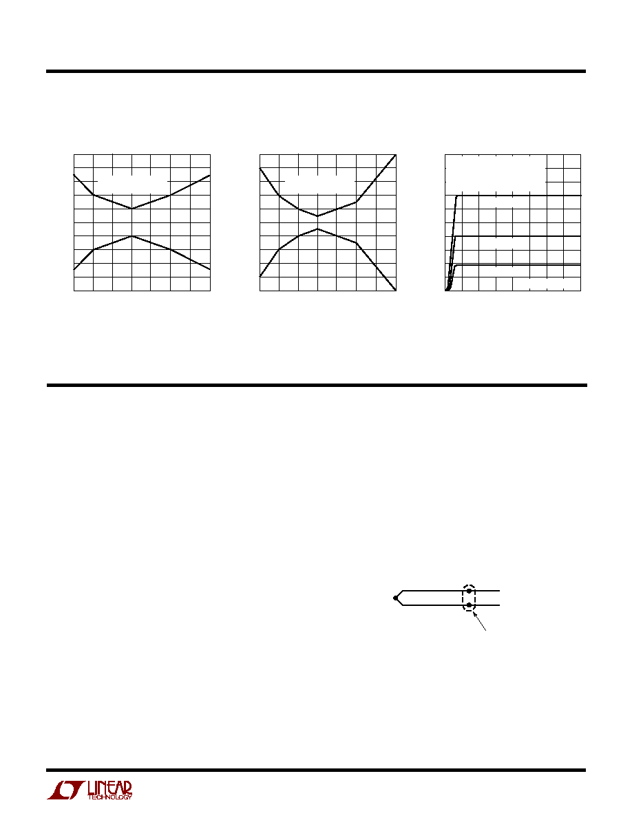
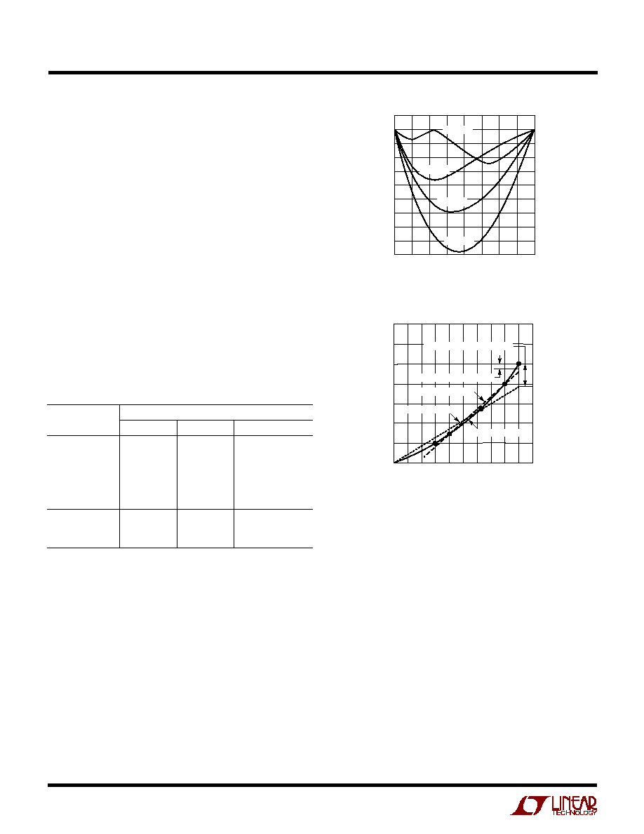
TYPICAL PERFOR A CE CHARACTERISTICS
U
W
10mV/
∞
C Output Temperature
Error LT1025
10mV/
∞
C Output Temperature
Error LT1025A
Supply Current
TEMPERATURE
TO BE MEASURED
T1
T2
Fe
Cu
Cu
CONSTANTAN
LT1025 MUST BE LOCATED
NEXT TO COLD JUNCTION
FOR TEMPERATURE TRACKING
V
S
}
LT1025 ∑ AG01
JUNCTION TEMPERATURE (
∞
C)
*ERROR CURVE FACTORS IN THE NONLINEARITY
TERM BUILT IN TO THE LT1025. SEE THEORY OF
OPERATION IN APPLICATION GUIDE SECTION
≠50
≠10
TEMPERATURE ERROR (
∞
C)
≠8
≠4
≠2
0
10
4
0
50
75
LT1025 ∑ G01
≠6
6
8
2
≠25
25
100
125
GUARANTEED LIMITS*
LT1025
JUNCTION TEMPERATURE (
∞
C)
*ERROR CURVE FACTORS IN THE NONLINEARITY
TERM BUILT IN TO THE LT1025. SEE THEORY OF
OPERATION IN APPLICATION GUIDE SECTION
≠50
≠5
TEMPERATURE ERROR (
∞
C)
≠4
≠2
≠1
0
5
2
0
50
75
LT1025 ∑ G02
≠3
3
4
1
≠25
25
100
125
GUARANTEED LIMITS*
LT1025A
SUPPLY VOLTAGE (V)
0
0
CURRENT (
µ
A)
20
60
80
100
200
140
10
20
25
LT1025 ∑ G03
40
160
180
120
5
15
30
35
40
DOES NOT INCLUDE 30
µ
A
PULL-DOWN CURRENT
REQUIRED FOR TEMPERATURES
BELOW 0
∞
C
T
J
= 125
∞
C
PIN 4 TIED TO PIN 5
T
J
= 25
∞
C
T
J
= ≠55
∞
C
The LT1025 was designed to be extremely easy to use, but
the following ideas and suggestions should be helpful in
obtaining the best possible performance and versatility
from this new cold junction compensator.
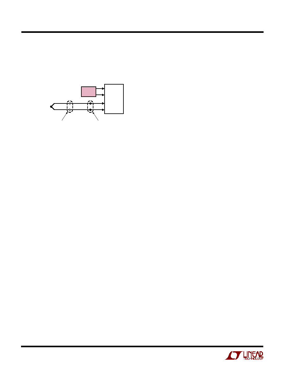
Theory of Operation
A thermocouple consists of two dissimilar metals joined
together. A voltage (Seebeck EMF) will be generated if the
two ends of the thermocouple are at different
temperatures. In Figure 1, iron and constantan are joined
at the temperature measuring point T1. Two additional
thermocouple junctions are formed where the iron and
constantan connect to ordinary copper wire. For the
purposes of this discussion it is assumed that these two
junctions are at the same temperature, T2. The Seebeck
voltage, V
S
, is the product of the Seebeck coefficient
,
and the temperature difference, T1 ≠ T2; V
S
=
(T1 ≠ T2).
The junctions at T2 are commonly called the cold junction
because a common practice is to immerse the T2 junction
in 0
∞
C ice/water slurry to make T2 independent of room
temperature variations. Thermocouple tables are based
on a cold-junction temperature of 0
∞
C.
To date, IC manufacturers efforts to make microminiature
thermos bottles have not been totally successful. There-
fore, an electronically simulated cold-junction is required
for most applications. The idea is basically to add a
temperature dependent voltage to V
S
such that the voltage
sum is the same as if the T2 junction were at a constant 0
∞
C
instead of at room temperature. This voltage source is
called a cold junction compensator. Its output is designed
to be 0V at 0
∞
C and have a slope equal to the Seebeck
coefficient over the expected range of T2 temperatures.
Figure 1
To operate properly, a cold junction compensator must be
at exactly the same temperature as the cold junction of the
thermocouple (T2).
Therefore, it is important to locate the
LT1025 physically close to the cold junction with local
temperature gradients minimized. If this is not possible,
APPLICATIO S I FOR ATIO
W
U
U
U
4
LT1025
1025fa
an extender made of matching thermocouple wire can be
used. This shifts the cold junction from the user termina-
tion to the end of the extender so that the LT1025 can be
located remotely from the user termination as shown in
Figure 2.
The four thermocouple outputs on the LT1025 are
60.9
µ
V/
∞
C (E), 51.7
µ
V/
∞
C (J), 40.6
µ
V/
∞
C (K and T), and
6
µ
V/
∞
C (R and S). These particular coefficients are chosen
to match the room temperature (25
∞
C) slope of the
thermocouples. Over wide temperature ranges, however,
the slope of thermocouples changes, yielding a quasi-
parabolic error compared to a constant slope. The LT1025
outputs have a deliberate parabolic "bow" to help
compensate for this effect. The outputs can be mathemati-
cally described as the sum of a linear term equal to room
temperature slope plus a quadratic term proportional to
temperature deviation from 25
∞
C
squared. The coefficient
(þ) of the quadratic term is a compromise value chosen to
offer improvement in all the outputs.
V
OUT
=
T +
þ(T ≠25
∞
)
2
þ
5.5 ∑ 10
≠ 4
The actual þ term which would be required to best
compensate each thermocouple type in the temperature
range of 0
∞
C to 50
∞
C is: E, 6.6 ∑ 10
≠4
; J, 4.8 ∑ 10
≠4
;
K, 4.3 ∑ 10
≠4
; R, 1.9 ∑ 10
≠3
, S, 1.9 ∑ 10
≠3
; T, 1 ∑ 10
≠3
.
The temperature error specification for the LT1025
10mV/
∞
C output (shown as a graph) assumes a þ of
5.5 ∑10
≠4
. For example, an LT1025 is considered "perfect"
if its 10mV/
∞
C output fits the equation V
O
= 10mV(T) +
(10mV)(5.5 ∑ 10
≠4
)(T ≠ 25
∞
C)
2
.
Operating at Negative Temperatures
The LT1025 is designed to operate with a single positive
supply. It therefore cannot deliver proper outputs for
temperatures below zero unless an external pull-down
resistor is added to the V
O
output. This resistor can be
connected to any convenient negative supply. It should be
selected to sink at least 30
µ
A of current. Suggested value
for a ≠ 5V supply is 150k
, and for a ≠ 15V supply, 470k
.
Smaller resistors must be used if an external load is
connected to the 10mV/
∞
C output. The LT1025 can source
up to 1mA of current, but there is a trade-off with internal
temperature rise.
Internal Temperature Rise
The LT1025 is specified for temperature accuracy assum-
ing no internal temperature rise. At low supply voltages
this rise is usually negligible (
0.05
∞
C at 5V), but at higher
supply voltages or with external loads or pull-down cur-
rent, internal rise could become significant. This effect can
be calculated from a simple thermal formula,
T = (
JA
)
(V
+
)(I
Q
+ I
L
), where
JA
is thermal resistance from junction
to ambient, (
130
∞
C/W), V
+
is the LT1025 supply voltage,
I
Q
is the LT1025 supply current (
80
µ
A) and I
L
is the total
load current including actual load to ground and any pull-
down current needed to generate negative outputs. A
sample calculation with a 15V supply and 50
µ
A pull-down
current would yield, (130
∞
C/W) (15V) (80
µ
A + 50
µ
A) =
0.32
∞
C. This is a significant rise in some applications. It
can be reduced by lowering supply voltage (a simple fix is
to insert a 10V zener in the V
IN
lead) or the system can be
calibrated and specified after an initial warm-up period of
several minutes.
Driving External Capacitance
The direct thermocouple drive pins on the LT1025 (J, K,
etc.) can be loaded with as much capacitance as desired,
but the 10mV/
∞
C output should not be loaded with more
than 50pF unless external pull-down current is added, or
a compensation network is used.
Thermocouple Effects in Leads
Thermocouple voltages are generated whenever dissimi-
lar materials are joined. This includes the leads of IC
packages, which may be kovar in TO-5 cans, alloy 42 or
copper in dual-in-line packages, and a variety of other
materials in plating finishes and solders. The net effect
of these thermocouples is "zero" if all are at exactly the
Figure 2
"HOT"
JUNCTION
Fe
Fe
CN
CN
EXTENDER
Cu
Cu
"NEW" COLD
JUNCTION
AMPLIFIER
FRONT PANEL
CONNECTOR
LT1025 ∑ AG02
LT1025
APPLICATIO S I FOR ATIO
W
U
U
U
5
LT1025
1025fa
same temperature, but temperature gradients exist within
IC packages and across PC boards whenever power is
dissipated. For this reason, extreme care must be used to
ensure that no temperature gradients exist in the vicinity
of the thermocouple terminations, the LT1025, or the
thermocouple amplifier. If a gradient cannot be eliminated,
leads should be positioned isothermally, especially the
LT1025 R
≠
and appropriate output pins, the amplifier input
pins, and the gain setting resistor leads. An effect to watch
for is amplifier offset voltage warm-up drift caused by
mismatched thermocouple materials in the wire-bond/
lead system of the IC package. This effect can be as high
as tens of microvolts in TO-5 cans with kovar leads. It has
nothing to do with the actual offset drift specification of the
amplifier and can occur in amplifiers with measured "zero"
drift. Warm-up drift is directly proportional to amplifier
power dissipation. It can be minimized by avoiding TO-5
cans, using low supply current amplifiers, and by using the
lowest possible supply voltages. Finally, it can be accom-
modated by calibrating and specifying the system after a
five minute warm-up period.
Reversing the Polarity of the 10mV/
∞
C Output
The LT1025 can be made to "stand on its head" to achieve
a minus 10mV/
∞
C output point. This is done as shown in
Figure 3. The normal output (V
O
) is grounded and feed-
back is established between the ground pin and the
positive supply pin by feeding both of them with currents
while coupling them with a 6V zener. The ground pin will
now be forced by feedback to generate ≠10mV/
∞
C
as long
as the grounded output is supplying a net "source" current
into ground. This condition is satisfied by selecting R1
such that the current through R1 (I
≠
) is more than the sum
of the LT1025 supply current, the maximum load current
(I
L
), and the minimum zener current (
50
µ
A). R2 is then
selected to supply more current than I
≠
.
R
V
A I
R
V
V
V
V R
A
L
Z
1
300
2
6
1 280
=
µ +
=
+
µ
+
≠
≠
,
≠
(
)
/
For
±
15V supplies, with I
L
= 20
µ
A maximum, R1 = 47k and
R2 = 15k.
Amplifier Considerations
Thermocouple amplifiers need very low offset voltage and
drift, and fairly low bias current if an input filter is used. The
best precision bipolar amplifiers should be used for type
J, K, E, and T thermocouples which have Seebeck coeffi-
cients of 40
µ
V/
∞
C to 60
µ
V/
∞
C. In particularly critical appli-
cations or for R and S thermocouples (6
µ
V/
∞
C to 15
µ
V/
∞
C),
a chopper-stabilized amplifier is required. Linear Technol-
ogy offers three amplifiers specifically tailored for thermo-
couple applications. The LTKA0x is a bipolar design with
extremely low offset (< 35
µ
V), low drift (<1.5
µ
V/
∞
C), very
low bias current (<1nA), and almost negligible warm-up
drift (supply current is
400
µ
A). It is very cost effective
even when compared with "jellybean" op amps with vastly
inferior specifications.
For the most demanding applications, the LTC1050 and
LTC1052 CMOS chopper-stabilized amplifiers offer 5
µ
V
offset and 0.05
µ
V/
∞
C drift (even over the full military
temperature range). Input bias current is 30pA, and gain
is typically 30 million. These amplifiers should be used for
R and S thermocouples, especially if no offset adjust-
ments can be tolerated, or a large ambient temperature
swing is expected.
Regardless of amplifier type, it is suggested that for best
possible performance, dual-in-line (DIP) packages be
used to avoid thermocouple effects in the kovar leads of
TO-5 metal can packages if amplifier supply current ex-
ceeds 500
µ
A. These leads can generate both DC and AC
offset terms in the presence of thermal gradients in the
package and/or external air motion.
APPLICATIO S I FOR ATIO
W
U
U
U
Figure 3
R2
15k
R1
47k
I
+
I
≠
V
+
(15V)
V
≠
(≠15V)
I
L
R
L
V
OUT
≠10mV/
∞
C
D1
V
Z
6V
LT1025 ∑ AG03
LT1025
GND
V
IN
V
O
6
LT1025
1025fa
Figure 4. Thermocouple Nonlinearity, 0
∞
C to 400
∞
C
Figure 5. Offset Curve Fitting
In many situations, thermocouples are used in high noise
environments, and some sort of input filter is required.
(See discussion of input filters). To reject 60Hz pick-up
with reasonable capacitor values, input resistors in the
10k-100k range are needed. Under these conditions, bias
current for the amplifier needs to be less than 1nA to avoid
offset and drift effects.
To avoid gain error, high open loop gain is necessary for
single-stage thermocouple amplifiers with 10mV/
∞
C or higher
outputs. A type K amplifier, for instance, with 100mV/
∞
C
output, needs a
closed loop gain of
2,500. An ordinary op
amp with a minimum open loop of 50,000 would have an
initial gain error of (2,500)/(50,000) = 5%! Although closed
loop gain is commonly trimmed, temperature drift of open
loop gain will have a very deleterious effect on output
accuracy. Minimum suggested open loop gain for type E, J,
K, and T thermocouples is 250,000. This gain is adequate for
type R and S if output scaling is 10mV/
∞
C or less.
Suggested Amplifier Types
SUPPLY VOLTAGE
THERMOCOUPLE
±
15V
±
5V
SINGLE SUPPLY
E, J, K, T
LTKA0x
LTKA0x
LTC1050
LT1012
LT1012
LTC1052
LT1001
LT1001
LT1006
LTC1050
LTC1052
LT1006
R, S
LTKA0x
LTC1050
LTC1050
LT1012
LTC1052
LTC1052
LTKA0x
LT1006
Thermocouple Nonlinearities
Thermocouples are linear over relatively limited temperature
spans if accuracies of better than 2
∞
C are needed. The graph
in Figure 4 shows thermocouple nonlinearity for the
temperature range of 0
∞
C to 400
∞
C. Nonlinearities can be
dealt with in hardware by using offsets, breakpoints, or power
series generators. Software solutions include look-up tables,
power series expansions, and piece-wise approximations.
For tables and power series coefficients, the reader is referred
to the ASTM Publication 470A.
Hardware correction for nonlinearity can be as simple as an
offset term. This is shown in Figure 5. The thermocouple
shown in the figure has an increasing slope (
) with
temperature. The temperature range of interest is between T
L
and T
H
, with a calibration point at T
M
. If a simple amplifier is
used and calibrated at T
M
, the output will be very high at T
L
and very low at T
H
. Adding the proper offset term and
calibrating at T1/6 or T5/6 can significantly reduce errors. The
technique is as follows:
1. Calculate amplifier gain:
G = (SF) (T
H
≠ T
L
)/(V
H
≠ V
L
)
SF = Output scale factor, e.g., 10mV/
∞
C
V
H
= Thermocouple output at T
H
V
L
= Thermocouple output at T
L
2. Use precision resistors to set gain or calibrate gain by
introducing a precision "delta" input voltage and trimming
for proper "delta" output.
APPLICATIO S I FOR ATIO
W
U
U
U
TEMPERATURE (
∞
C)
0
ERROR TYPE E AND T (
∞
C)
20
15
12.5
10
5
100
200
250
LT1025 ∑ G04
17.5
2.5
0
7.5
8
6
5
4
2
7
1
0
3
ERROR TYPE J AND K (
∞
C)
50
150
300 350
400
K
SCALE
J
SCALE
SCALE
E
SCALE
T
TEMPERATURE (
∞
C)
0
OUTPUT (V)
V
L
V
H
LT1025 ∑ G05
T1/6
T
H
T
L
T
M
T5/6
THERMOCOUPLE
SIMPLE AMPLIFIER
OFFSET AMPLIFIER
ERROR AFTER OFFSETTING
ERROR BEFORE OFFSETTING
7
LT1025
1025fa
3. Calibrate output by adding in a true offset term which
does not affect gain (by summing, etc.). Calibration may
be done at any temperature either by immersing the
thermocouple in a calibrated bath or by substituting a
precision input voltage. The method which tends to
minimize worst-case error over the whole T
L
to T
H
range
is to calibrate at 1/6 or 5/6 of span. This may be modified
if best accuracy is desired at one particular point.
Breakpoint correction for nonlinearity is more compli-
cated than a simple offset, but a single breakpoint com-
bined with offset will reduce errors typically by 4:1 over a
simple offset technique.
APPLICATIO S I FOR ATIO
W
U
U
U
TYPICAL APPLICATIO S
U
≠
≠
+
+
4
6
7
2
3
≠15V
15V
≠15V
≠10mV/
∞
C
15V
3k
300k
GND
R
≠
K
TYPE K
C1
0.1
µ
F
C2
1
µ
F
V
IN
V
O
V
OUT
LT1025
LTKA0x
OR EQUIVALENT. SEE "AMPLIFIER CONSIDERATIONS"
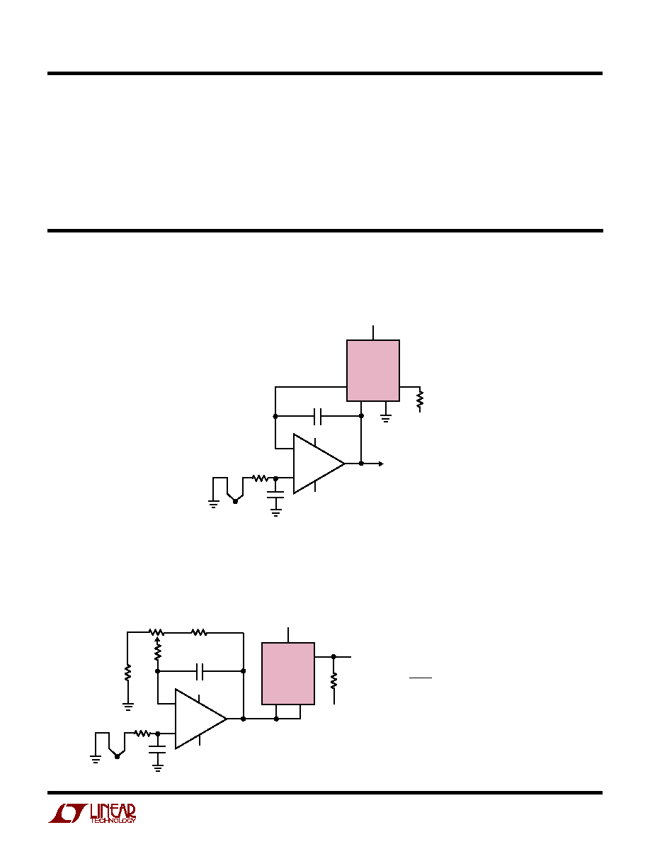
Eliminating Amplifier Feedback Resistors
(Output Goes Negative with Increasing Temperature)
Type K Thermometer with Grounded Thermocouple
≠15V
10mV/
∞
C
V
OUT
V
+
V
≠
V
≠
V
≠
GND
R
≠
LT1025
≠
+
V
+
R5
10k
R1
1k
1%
R6
9.1k
R4*
470k
R3
255k
1%
R2
100
TYPE K
0.1
µ
F
C2
1
µ
F
*R4
30
µ
A
MUST BE DECREASED APPROPRIATELY. R4 IS NOT
REQUIRED (OPEN) FOR LT1025 TEMPERATURES
0
∞
C
WHEN SOURCING CURRENT ONLY
OR EQUIVALENT. SEE "AMPLIFIER CONSIDERATIONS"
V
IN
V
O
IF OUTPUT MUST SINK CURRENT, R4
LTKA0x
8
LT1025
1025fa
TYPICAL APPLICATIO S
U
V
OUT
10mV/
∞
C
0
∞
C TO 500
∞
C
R5
47k
R1
1k
1%
R7
15k
R3
141k
1%
R2
100
R4
141k
C1
0.1
µ
F
GND
LT1025
≠15V
≠
≠
+
+
15V
6V
15V
≠15V
R6
10k
TYPE E
1
µ
F
*SEE "REVERSING THE POLARITY OF THE 10mV/
∞
C OUTPUT"
OR EQUIVALENT. SEE "AMPLIFIER CONSIDERATIONS"
LTKA0x
≠10mV/
∞
C
V
IN
V
O
Utilizing Negative LT1025 Drive to Accommodate Grounded Thermocouple*
R6
7.5k
1%
R7
500
FULL-SCALE
TRIM
5V**
V
≠
V
≠
V
+
GND
V
IN
V
O
LT1025
R9
100k
R5
3k
≠
+
TYPE K
≠15V
≠
+
LTKA0x
10mV/
∞
C
V
OUT
V
CM
10mV/
∞
C
C1*
C2*
R3
1M
0.1%
R1
10k
0.1%
R2
10k
0.1%
R4
1M
0.1%
R8
5k
1%
=
(V
≠
)(10k)
V
OUT
(MAX)
*C1 AND C2 FILTER RIPPLE AND NOISE, BUT WILL LIMIT AC COMMON-MODE REJECTION
IF NOT MATCHED. SUGGESTED VALUES ARE 0.001
µ
F TO 0.1
µ
F
**USE LOWEST POSSIBLE SUPPLY VOLTAGE TO MINIMIZE INTERNAL TEMPERATURE RISE
FOR BEST ACCURACY, THERMOCOUPLE RESISTANCE SHOULD BE LESS THAN 100
OR EQUIVALENT. SEE "AMPLIFIER CONSIDERATIONS"
Differential Thermocouple Amplifier
9
LT1025
1025fa
TYPICAL APPLICATIO S
U
Type S Thermocouple Amplifier with Ultralow Offset and Drift
+
≠
* TRIM R5 FOR V
OUT
= 1.669V AT V
IN
= 0.000mV (+INPUT OF AMPLIFIER GROUNDED)
** TRIM R2 FOR V
OUT
= 9.998V AT T = 1000
∞
C, OR FOR V
IN
AT +INPUT OF AMPLIFIER = 9.585mV
THIS AMPLIFIER HAS A DELIBERATE OFFSET TO ALLOW OUTPUT SLOPE (10mV/
∞
C) TO BE SET
INDEPENDENTLY FROM AN ARBITRARY HIGH TEMPERATURE CENTER POINT (1000
∞
C). THIS IS
REQUIRED BECAUSE THE SLOPE OF TYPE "S" THERMOCOUPLES VARIES RAPIDLY WITH
TEMPERATURE, INCREASING FROM 6
µ
V/
∞
C AT 25
∞
C to 11
µ
V/
∞
C AT 1000
∞
C. NONLINEARITY LIMITS
ACCURACY TO
3
∞
C OVER THE 800
∞
C TO 1200
∞
C RANGE EVEN WITH OFFSET CORRECTION
V
+
V
+
V
≠
TYPE S
R7
750k
R6
12k
≠15V
LT1009
2.5V
R4
1.37M
1%
R1
1k
1%
R2**
100
FULL-SCALE
TRIM
R3
909k
1%
0.1
µ
F
0.1
µ
F
1
4
8
6
7
3
5
2
R5*
10k
OFFSET
TRIM
R4
2.7k
1
µ
F
0.1
µ
F
15V
V
OUT
10mV/
∞
C
800
∞
C TO 1200
∞
C
V
IN
V
O
LT1025
LT1052
GND
R
≠
R,S
≠
+
LT1025 ∑ TA06
10
LT1025
1025fa
U
PACKAGE DESCRIPTIO
J8 Package
8-Lead CERDIP (Narrow 0.300, Hermetic)
(LTC DWG # 05-08-1110)
J8 1298
0.014 ≠ 0.026
(0.360 ≠ 0.660)
0.200
(5.080)
MAX
0.015 ≠ 0.060
(0.381 ≠ 1.524)
0.125
3.175
MIN
0.100
(2.54)
BSC
0.300 BSC
(0.762 BSC)
0.008 ≠ 0.018
(0.203 ≠ 0.457)
0
∞
≠ 15
∞
0.005
(0.127)
MIN
0.405
(10.287)
MAX
0.220 ≠ 0.310
(5.588 ≠ 7.874)
1
2
3
4
8
7
6
5
0.025
(0.635)
RAD TYP
0.045 ≠ 0.068
(1.143 ≠ 1.727)
FULL LEAD
OPTION
0.023 ≠ 0.045
(0.584 ≠ 1.143)
HALF LEAD
OPTION
CORNER LEADS OPTION
(4 PLCS)
0.045 ≠ 0.065
(1.143 ≠ 1.651)
NOTE: LEAD DIMENSIONS APPLY TO SOLDER DIP/PLATE
OR TIN PLATE LEADS
OBSOLETE PACKAGE

11
LT1025
1025fa
Information furnished by Linear Technology Corporation is believed to be accurate and reliable.
However, no responsibility is assumed for its use. Linear Technology Corporation makes no represen-
tation that the interconnection of its circuits as described herein will not infringe on existing patent rights.
U
PACKAGE DESCRIPTIO
N8 Package
8-Lead PDIP (Narrow 0.300)
(LTC DWG # 05-08-1510)
N8 1098
0.100
(2.54)
BSC
0.065
(1.651)
TYP
0.045 ≠ 0.065
(1.143 ≠ 1.651)
0.130
±
0.005
(3.302
±
0.127)
0.020
(0.508)
MIN
0.018
±
0.003
(0.457
±
0.076)
0.125
(3.175)
MIN
1
2
3
4
8
7
6
5
0.255
±
0.015*
(6.477
±
0.381)
0.400*
(10.160)
MAX
0.009 ≠ 0.015
(0.229 ≠ 0.381)
0.300 ≠ 0.325
(7.620 ≠ 8.255)
0.325
+0.035
≠0.015
+0.889
≠0.381
8.255
(
)
*THESE DIMENSIONS DO NOT INCLUDE MOLD FLASH OR PROTRUSIONS.
MOLD FLASH OR PROTRUSIONS SHALL NOT EXCEED 0.010 INCH (0.254mm)

12
LT1025
1025fa
+
≠
* FOR BEST ACCURACY, THERMOCOUPLE RESISTANCE
SHOULD BE LESS THAN 50
** SELECTED FOR 0
∞
C TO 200
∞
C RANGE
OR EQUIVALENT. SEE "AMPLIFIER CONSIDERATIONS"
V
+
V
+
V
≠
R1
10k
1%
FULL-SCALE
ADJUST
V
OUT
10mV/
∞
C
LTKA0x
R7
6.8k
R4
10k
R5
2k
R3
1M
1%
C1
0.01
µ
F
R6**
8.4k
C2
0.01
µ
F
TYPE J*
V
IN
J
LT1025
GND
R
≠
≠
+
LT1025 ∑ TA07
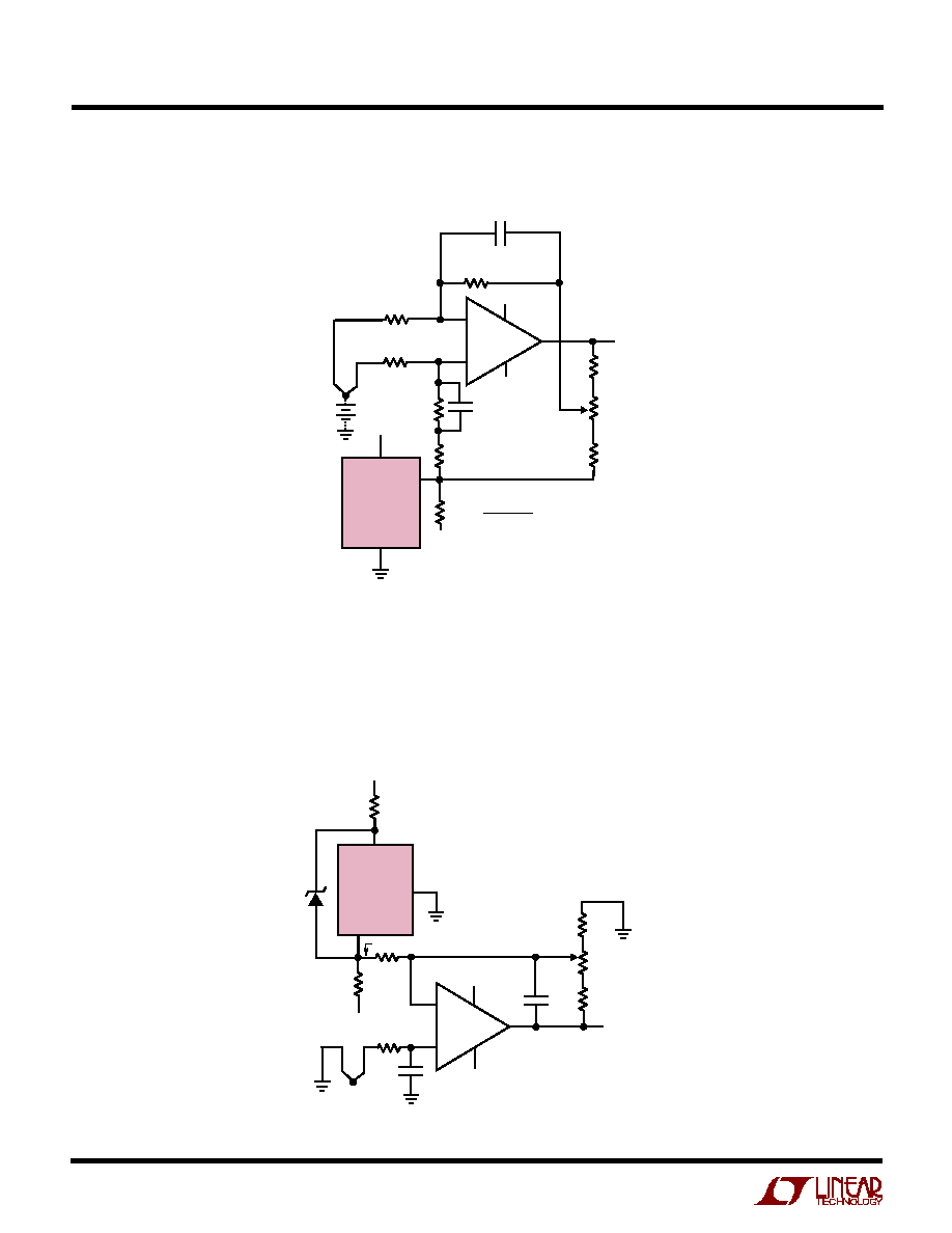
Grounded Thermocouple Amplifier with Positive Output
Linear Technology Corporation
1630 McCarthy Blvd., Milpitas, CA 95035-7417
(408) 432-1900
q
FAX: (408) 434-0507
q
www.linear.com
LW/CPI 1001 1.5K REV A ∑ PRINTED IN USA
©
LINEAR TECHNOLOGY CORPORATION 1988
TYPICAL APPLICATIO
U
PART NUMBER
DESCRIPTION
COMMENTS
LT1012
Picoamp Input Current Op Amp
120
µ
V Max V
OS
, 280pA Max I
OS
LTC1050
Zero Drift Amplifier
5
µ
V Max V
OS
, A
VOL
1V/
µ
V Max
LTC2050
SOT-23 Zero Drift Amplifier
3
µ
V Max V
OS
RELATED PARTS