 | –≠–ª–µ–∫—Ç—Ä–æ–Ω–Ω—ã–π –∫–æ–º–ø–æ–Ω–µ–Ω—Ç: LT1028A | –°–∫–∞—á–∞—Ç—å:  PDF PDF  ZIP ZIP |
1
LT1028/LT1128
FEATURES
DESCRIPTIO
U
APPLICATIO S
U
s
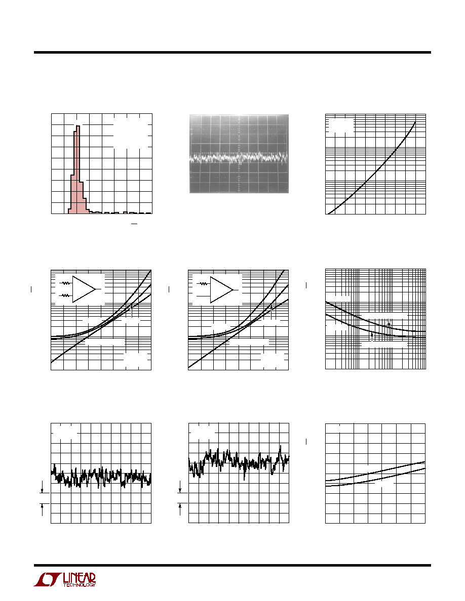
Voltage Noise
1.1nV/
Hz Max at 1kHz
0.85nV/
Hz Typ at 1kHz
1.0nV/
Hz Typ at 10Hz
35nV
P-P
Typ, 0.1Hz to 10Hz
s
Voltage and Current Noise 100% Tested
s
Gain-Bandwidth Product
LT1028: 50MHz Min
LT1128: 13MHz Min
s
Slew Rate
LT1028: 11V/
µ
s Min
LT1128: 5V/
µ
s Min
s
Offset Voltage: 40
µ
V Max
s
Drift with Temperature: 0.8
µ
V/
∞
C Max
s
Voltage Gain: 7 Million Min
s
Available in 8-Pin SO Package
The LT
Æ
1028(gain of ≠1 stable)/LT1128(gain of +1 stable)
achieve a new standard of excellence in noise performance
with 0.85nV/
Hz 1kHz noise, 1.0nV/
Hz 10Hz noise. This
ultralow noise is combined with excellent high speed
specifications (gain-bandwidth product is 75MHz for
LT1028, 20MHz for LT1128), distortion-free output, and
true precision parameters (0.1
µ
V/
∞
C drift, 10
µ
V offset
voltage, 30 million voltage gain). Although the LT1028/
LT1128 input stage operates at nearly 1mA of collector
current to achieve low voltage noise, input bias current is
only 25nA.
The LT1028/LT1128's voltage noise is less than the noise
of a 50
resistor. Therefore, even in very low source
impedance transducer or audio amplifier applications, the
LT1028/LT1128's contribution to total system noise will
be negligible.
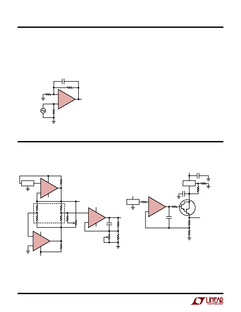
Ultralow Noise Precision
High Speed Op Amps
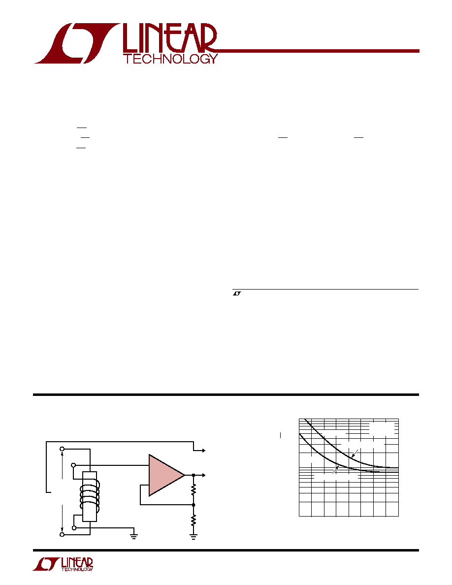
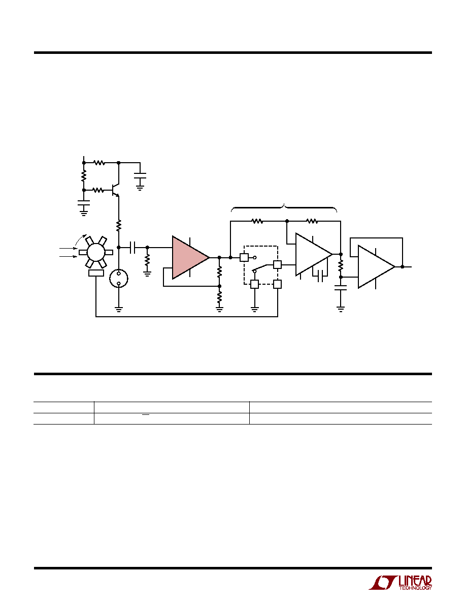
Flux Gate Amplifier
Voltage Noise vs Frequency
≠
+
DEMODULATOR
SYNC
OUTPUT TO
DEMODULATOR
LT1028
1k
50
SQUARE
WAVE
DRIVE
1kHz
FLUX GATE
TYPICAL
SCHONSTEDT
#203132
1028/1128 TA01
FREQUENCY (Hz)
1
0.1
1
10
10
100
1028/1128 TA02
VOLTAGE NOISE DENSITY (nV/
Hz)
0.1
1k
1/f CORNER = 3.5Hz
1/f CORNER = 14Hz
TYPICAL
MAXIMUM
V
S
=
±
15V
T
A
= 25
∞
C
s
Low Noise Frequency Synthesizers
s
High Quality Audio
s
Infrared Detectors
s
Accelerometer and Gyro Amplifiers
s
350
Bridge Signal Conditioning
s
Magnetic Search Coil Amplifiers
s
Hydrophone Amplfiers
TYPICAL APPLICATIO
U
, LTC and LT are registered trademarks of Linear Technology Corporation
2
LT1028/LT1128
Supply Voltage
≠55
∞
C to 105
∞
C ................................................
±
22V
105
∞
C to 125
∞
C ................................................
±
16V
Differential Input Current (Note 9) ......................
±
25mA
Input Voltage ............................ Equal to Supply Voltage
Output Short Circuit Duration .......................... Indefinite
A
U
G
W
A
W
U
W
A
R
BSOLUTE
XI
TI
S
Operating Temperature Range
LT1028/LT1128AM, M (OBSOLETE) . ≠ 55
∞
C to 125
∞
C
LT1028/LT1128AC, C (Note 11) ......... ≠ 40
∞
C to 85
∞
C
Storage Temperature Range
All Devices ........................................ ≠ 65
∞
C to 150
∞
C
Lead Temperature (Soldering, 10 sec.)................. 300
∞
C
W
U
U
PACKAGE/ORDER I FOR ATIO
S8 PART MARKING
LT1028CS8
LT1128CS8
ORDER PART
NUMBER
ORDER PART
NUMBER
ORDER PART
NUMBER
1
2
3
4
5
6
7
8
TOP VIEW
≠IN
+IN
V
≠
S8 PACKAGE
8-LEAD PLASTIC SOIC
V+
OUT
+
≠
V
OS
TRIM
V
OS
TRIM
OVER-
COMP
1028
1128
LT1028AMH
LT1028MH
LT1028ACH
LT1028CH
LT1028AMJ8
LT1028MJ8
LT1028ACJ8
LT1028CJ8
LT1128AMJ8
LT1128MJ8
LT1128CJ8
LT1028CSW
TOP VIEW
V
+
V
OS
TRIM
≠IN
OUT
OVER-
COMP
+IN
V
≠
(CASE)
8
7
5
3
2
1
4
H PACKAGE
8-LEAD TO-5 METAL CAN
V
OS
TRIM
+
≠
6
N8 PACKAGE
8-LEAD PLASTIC DIP
1
2
3
4
5
6
7
8
TOP VIEW
≠IN
+IN
V
≠
V+
OUT
+
≠
J8 PACKAGE
8-LEAD CERAMIC DIP
OVER-
COMP
V
OS
TRIM
V
OS
TRIM
TOP VIEW
SW PACKAGE
16-LEAD PLASTIC SOL
1
2
3
4
5
6
7
8
16
15
14
13
12
11
10
9
NC
NC
TRIM
≠IN
+IN
V
≠
NC
NC
NC
NC
TRIM
V
+
OUT
NC
NC
NOTE: THIS DEVICE IS NOT RECOM-
MENDED FOR NEW DESIGNS
OVER-
COMP
+
≠
Consult LTC Marketing for parts specified with wider operating temperature ranges.
(Note 1)
OBSOLETE PACKAGE
T
JMAX
= 175
∞
C,
JA
= 140
∞
C/W,
JC
= 40
∞
C/W
T
JMAX
= 140
∞
C,
JA
= 130
∞
C/W
T
JMAX
= 165
∞
C,
JA
= 100
∞
C/W
LT1028ACN8
LT1028CN8
LT1128ACN8
LT1128CN8
T
JMAX
= 130
∞
C,
JA
= 130
∞
C/W
Consider S8 or N8 Packages for Alternate Source
T
JMAX
= 135
∞
C,
JA
= 140
∞
C/W
OBSOLETE PACKAGE
Consider N8 Package for Alternate Source
ORDER PART
NUMBER
3
LT1028/LT1128
SYMBOL PARAMETER
CONDITIONS
MIN
TYP
MAX
MIN
TYP
MAX
UNITS
V
OS
Input Offset Voltage
(Note 2)
10
40
20
80
µ
V
V
OS
Long Term Input Offset
(Note 3)
0.3
0.3
µ
V/Mo
Time
Voltage Stability
I
OS
Input Offset Current
V
CM
= 0V
12
50
18
100
nA
I
B
Input Bias Current
V
CM
= 0V
±
25
±
90
±
30
±
180
nA
e
n
Input Noise Voltage
0.1Hz to 10Hz (Note 4)
35
75
35
90
nV
P-P
Input Noise Voltage Density
f
O
= 10Hz (Note 5)
1.00
1.7
1.0
1.9
nV/
Hz
f
O
= 1000Hz, 100% tested
0.85
1.1
0.9
1.2
nV/
Hz
I
n
Input Noise Current Density
f
O
= 10Hz (Note 4 and 6)
4.7
10.0
4.7
12.0
pA/
Hz
f
O
= 1000Hz, 100% tested
1.0
1.6
1.0
1.8
pA/
Hz
Input Resistance
Common Mode
300
300
M
Differential Mode
20
20
k
Input Capacitance
5
5
pF
Input Voltage Range
±
11.0
±
12.2
±
11.0
±
12.2
V
CMRR
Common Mode Rejection Ratio
V
CM
=
±
11V
114
126
110
126
dB
PSRR
Power Supply Rejection Ratio
V
S
=
±
4V to
±
18V
117
133
110
132
dB
A
VOL
Large-Signal Voltage Gain
R
L
2k, V
O
=
±
12V
7.0
30.0
5.0
30.0
V/
µ
V
R
L
1k, V
O
=
±
10V
5.0
20.0
3.5
20.0
V/
µ
V
R
L
600
, V
O
=
±
10V
3.0
15.0
2.0
15.0
V/
µ
V
V
OUT
Maximum Output Voltage Swing
R
L
2k
±
12.3
±
13.0
±
12.0
±
13.0
V
R
L
600
±
11.0
±
12.2
±
10.5
±
12.2
V
SR
Slew Rate
A
VCL
= ≠1
LT1028
11.0
15.0
11.0
15.0
V/
µ
s
A
VCL
= ≠1
LT1128
5.0
6.0
4.5
6.0
V/
µ
s
GBW
Gain-Bandwidth Product
f
O
= 20kHz (Note 7)
LT1028
50
75
50
75
MHz
f
O
= 200kHz (Note 7)
LT1128
13
20
11
20
MHz
Z
O
Open-Loop Output Impedance
V
O
= 0, I
O
= 0
80
80
I
S
Supply Current
7.4
9.5
7.6
10.5
mA
ELECTRICAL C
C
HARA TERISTICS
V
S
=
±
15V, T
A
= 25
∞
C, unless otherwise noted.
LT1028AM/AC
LT1128AM/AC
LT1028M/C
LT1128M/C
SYMBOL PARAMETER
CONDITIONS
MIN
TYP
MAX
MIN
TYP
MAX
UNITS
V
OS
Input Offset Voltage
(Note 2)
q
30
120
45
180
µ
V
V
OS
Average Input Offset Drift
(Note 8)
q
0.2
0.8
0.25
1.0
µ
V/
∞
C
Temp
I
OS
Input Offset Current
V
CM
= 0V
q
25
90
30
180
nA
I
B
Input Bias Current
V
CM
= 0V
q
±
40
±
150
±
50
±
300
nA
Input Voltage Range
q
±
10.3
±
11.7
±
10.3
±
11.7
V
CMRR
Common Mode Rejection Ratio
V
CM
=
±
10.3V
q
106
122
100
120
dB
PSRR
Power Supply Rejection Ratio
V
S
=
±
4.5V to
±
16V
q
110
130
104
130
dB
A
VOL
Large-Signal Voltage Gain
R
L
2k, V
O
=
±
10V
q
3.0
14.0
2.0
14.0
V/
µ
V
R
L
1k, V
O
=
±
10V
2.0
10.0
1.5
10.0
V/
µ
V
V
OUT
Maximum Output Voltage Swing
R
L
2k
q
±
10.3
±
11.6
±
10.3
±
11.6
V
I
S
Supply Current
q
8.7
11.5
9.0
13.0
mA
LT1028AM
LT1128AM
LT1028M
LT1128M
ELECTRICAL C
C
HARA TERISTICS
The
q
denotes the specifications which apply over the temperature range
≠55
∞
C
T
A
125
∞
C. V
S
=
±
15V, unless otherwise noted.
4
LT1028/LT1128
SYMBOL PARAMETER
CONDITIONS
MIN
TYP
MAX
MIN
TYP
MAX
UNITS
V
OS
Input Offset Voltage
(Note 2)
q
15
80
30
125
µ
V
V
OS
Average Input Offset Drift
(Note 8)
q
0.1
0.8
0.2
1.0
µ
V/
∞
C
Temp
I
OS
Input Offset Current
V
CM
= 0V
q
15
65
22
130
nA
I
B
Input Bias Current
V
CM
= 0V
q
±
30
±
120
±
40
±
240
nA
Input Voltage Range
q
±
10.5
±
12.0
±
10.5
±
12.0
V
CMRR
Common Mode Rejection Ratio
V
CM
=
±
10.5V
q
110
124
106
124
dB
PSRR
Power Supply Rejection Ratio
V
S
=
±
4.5V to
±
18V
q
114
132
107
132
dB
A
VOL
Large-Signal Voltage Gain
R
L
2k, V
O
=
±
10V
q
5.0
25.0
3.0
25.0
V/
µ
V
R
L
1k, V
O
=
±
10V
4.0
18.0
2.5
18.0
V/
µ
V
V
OUT
Maximum Output Voltage Swing
R
L
2k
q
±
11.5
±
12.7
±
11.5
±
12.7
V
R
L
600
(Note 10)
±
9.5
±
11.0
±
9.0
±
10.5
V
I
S
Supply Current
q
8.0
10.5
8.2
11.5
mA
LT1028AC
LT1128AC
LT1028C
LT1128C
ELECTRICAL C
C
HARA TERISTICS
SYMBOL PARAMETER
CONDITIONS
MIN
TYP
MAX
MIN
TYP
MAX
UNITS
V
OS
Input Offset Voltage
q
20
95
35
150
µ
V
V
OS
Average Input Offset Drift
(Note 8)
q
0.2
0.8
0.25
1.0
µ
V/
∞
C
Temp
I
OS
Input Offset Current
V
CM
= 0V
q
20
80
28
160
nA
I
B
Input Bias Current
V
CM
= 0V
q
±
35
±
140
±
45
±
280
nA
Input Voltage Range
q
±
10.4
±
11.8
±
10.4
±
11.8
V
CMRR
Common Mode Rejection Ratio
V
CM
=
±
10.5V
q
108
123
102
123
dB
PSRR
Power Supply Rejection Ratio
V
S
=
±
4.5V to
±
18V
q
112
131
106
131
dB
A
VOL
Large-Signal Voltage Gain
R
L
2k, V
O
=
±
10V
q
4.0
20.0
2.5
20.0
V/
µ
V
R
L
1k, V
O
=
±
10V
3.0
14.0
2.0
14.0
V/
µ
V
V
OUT
Maximum Output Voltage Swing
R
L
2k
q
±
11.0
±
12.5
±
11.0
±
12.5
V
I
S
Supply Current
q
8.5
11.0
8.7
12.5
mA
LT1028AC
LT1128AC
LT1028C
LT1128C
ELECTRICAL C
C
HARA TERISTICS
on an RMS basis) is divided by the sum of the two source resistors to
obtain current noise. Maximum 10Hz current noise can be inferred from
100% testing at 1kHz.
Note 7: Gain-bandwidth product is not tested. It is guaranteed by design
and by inference from the slew rate measurement.
Note 8: This parameter is not 100% tested.
Note 9: The inputs are protected by back-to-back diodes. Current-limiting
resistors are not used in order to achieve low noise. If differential input
voltage exceeds
±
1.8V, the input current should be limited to 25mA.
Note 10: This parameter guaranteed by design, fully warmed up at T
A
=
70
∞
C. It includes chip temperature increase due to supply and load
currents.
Note 11: The LT1028/LT1128 are designed, characterized and expected to
meet these extended temperature limits, but are not tested at ≠40
∞
C and
85
∞
C. Guaranteed I grade parts are available. Consult factory.
Note 1: Absolute Maximum Ratings are those values beyond which the life
of a device may be impaired.
Note 2: Input Offset Voltage measurements are performed by automatic
test equipment approximately 0.5 sec. after application of power. In
addition, at T
A
= 25
∞
C, offset voltage is measured with the chip heated to
approximately 55
∞
C to account for the chip temperature rise when the
device is fully warmed up.
Note 3: Long Term Input Offset Voltage Stability refers to the average
trend line of Offset Voltage vs. Time over extended periods after the first
30 days of operation. Excluding the initial hour of operation, changes in
V
OS
during the first 30 days are typically 2.5
µ
V.
Note 4: This parameter is tested on a sample basis only.
Note 5: 10Hz noise voltage density is sample tested on every lot with the
exception of the S8 and S16 packages. Devices 100% tested at 10Hz are
available on request.
Note 6: Current noise is defined and measured with balanced source
resistors. The resultant voltage noise (after subtracting the resistor noise
The
q
denotes the specifications which apply over the temperature range
0
∞
C
T
A
70
∞
C. V
S
=
±
15V, unless otherwise noted.
The
q
denotes the specifications which apply over the temperature range
≠ 40
∞
C
T
A
85
∞
C. V
S
=
±
15V, unless otherwise noted. (Note 11)
5
LT1028/LT1128
C
C
HARA TERISTICS
U
W
A
TYPICAL PERFOR
CE
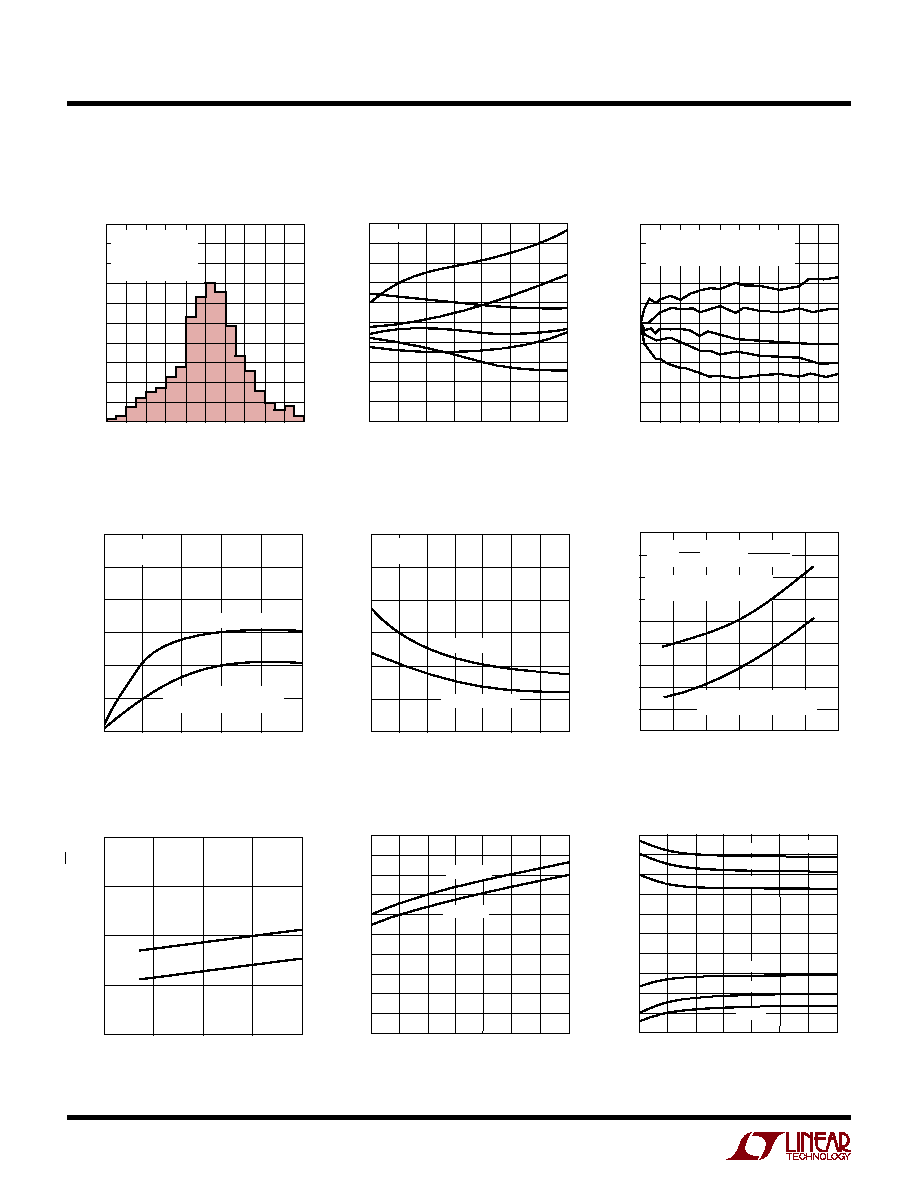
10Hz Voltage Noise Distribution
Total Noise vs Matched Source
Resistance
Total Noise vs Unmatched
Source Resistance
Current Noise Spectrum
0.01Hz to 1Hz Voltage Noise
TEMPERATURE (
∞
C)
≠50
0
RMS VOLTAGE DENSITY (nV/
Hz)
0.8
2.0
0
50
75
LT1028/1128 ∑ TPC09
O.4
1.6
1.2
≠25
25
100
125
V
S
=
±
15V
AT 10Hz
AT 1kHz
Voltage Noise vs Temperature
0.1Hz to 10Hz Voltage Noise
TIME (SEC)
0
8
LT1028/1128 ∑ TPC07
2
4
6
10
10nV
V
S
=
±
15V
T
A
= 25
∞
C
Wideband Noise, DC to 20kHz
BANDWIDTH (Hz)
100
RMS VOLTAGE NOISE (
µ
V)
0.1
1
100k
1M
10M
LT1028/1128 ∑ TPC03
0.01
10
10k
1k
V
S
=
±
15V
T
A
= 25
∞
C
Wideband Voltage Noise
(0.1Hz to Frequency Indicated)
MATCHED SOURCE RESISTANCE (
)
1
TOTAL NOISE DENSITY (nV/
Hz)
10
100
3
1k
10k
LT1028/1128 ∑ TPC04
1
0.1
V
S
=
±
15V
T
A
= 25
∞
C
10
30
100 300
3k
AT 10Hz
2 R
S
NOISE ONLY
AT 1kHz
≠
+
R
S
R
S
UNMATCHED SOURCE RESISTANCE (
)
1
TOTAL NOISE DENSITY (nV/
Hz)
10
100
3
1k
10k
LT1028/1128 ∑ TPC05
1
0.1
V
S
=
±
15V
T
A
= 25
∞
C
10
30
100 300
3k
AT 10Hz
2 R
S
NOISE ONLY
AT 1kHz
R
S
TIME (SEC)
0
80
LT1028/1128 ∑ TPC08
20
40
60
100
10nV
V
S
=
±
15V
T
A
= 25
∞
C
FREQUENCY (Hz)
10
0.1
CURRENT NOISE DENSITY (pA/
Hz)
1
10
100
100
1k
10k
LT1028/1128 ∑ TPC06
MAXIMUM
TYPICAL
1/f CORNER = 800Hz
1/f CORNER = 250Hz
0.6
0
NUMBER OF UNITS
20
60
80
100
1.0
1.4
1.8
180
LT1020/1120 ∑ TPC01
40
0.8
1.2
120
140
160
1.6
2.0
2.2
8
70
148
158
57
28
7 423 2 2 2
1
3 2 1 1 1
V
S
=
±
15V
T
A
= 25
∞
C
500 UNITS
MEASURED
FROM 4 RUNS
VOLTAGE NOISE DENSITY (nV/
Hz)
VERTICAL SCALE = 0.5
µ
V/DIV
HORIZONTAL SCALE = 0.5ms/DIV
6
LT1028/LT1128
OFFSET VOLTAGE (
µ
V)
≠50
UNITS (%)
12
16
20
30
LT1028/1128 ∑ TPC10
8
4
0
≠30
≠10
10
50
10
14
18
6
2
20
≠40
≠20
0
40
V
S
=
±
15V
T
A
= 25
∞
C
800 UNITS TESTED
FROM FOUR RUNS
C
C
HARA TERISTICS
U
W
A
TYPICAL PERFOR
CE
Supply Current vs Temperature
SUPPLY VOLTAGE (V)
0
RMS VOLTAGE NOISE DENSITY (nV/
Hz)
1.0
1.25
±
15
LT1028/1128 ∑ TPC16
0.75
0.5
±
5
±
10
±
20
1.5
T
A
= 25
∞
C
AT 10Hz
AT 1kHz
Voltage Noise vs Supply Voltage
TIME AFTER POWER ON (MINUTES)
0
0
CHANGE IN OFFSET VOLTAGE (
µ
V)
4
8
12
16
20
24
1
2
3
4
LT1028/1128 ∑ TPC13
5
V
S
=
±
15V
T
A
= 25
∞
C
METAL CAN (H) PACKAGE
DUAL-IN-LINE PACKAGE
PLASTIC (N) OR CERDIP (J)
TEMPERATURE (
∞
C)
≠50
0
SUPPLY CURRENT (mA)
1
3
4
5
10
7
0
50
75
LT1028/1128 ∑ TPC17
2
8
9
6
≠25
25
100
125
V
S
=
±
15V
V
S
=
±
5V
Bias Current Over the Common
Mode Range
Warm-Up Drift
Output Short-Circuit Current
vs Time
TIME FROM OUTPUT SHORT TO GROUND (MINUTES)
0
≠50
SINKING
≠40
≠20
≠10
0
50
20
2
LT1028/1128 ∑ TPC18
≠30
30
40
10
1
3
SHORT-CIRCUIT CURRENT (mA)
SOURCING
V
S
=
±
15V
≠50
∞
C
25
∞
C
125
∞
C
≠50
∞
C
125
∞
C
25
∞
C
Distribution of Input Offset
Voltage
Input Bias and Offset Currents
Over Temperature
TEMPERATURE (∞C)
≠50
INPUT BIAS AND OFFSET CURRENTS (nA)
40
50
60
25
75
LT1028/1128 ∑ TPC14
30
20
≠25
0
50
100
125
10
0
V
S
=
±
15V
V
CM
= 0V
BIAS CURRENT
OFFSET CURRENT
TEMPERATURE (
∞
C)
≠50
≠50
OFFSET VOLTAGE (
µ
V)
≠40
≠20
≠10
0
50
20
0
50
75
LT1028/1128 ∑ TPC11
≠30
30
40
10
≠25
25
100
125
V
S
=
±
15V
Long-Term Stability of Five
Representative Units
TIME (MONTHS)
0
OFFSET VOLTAGE CHANGE (
µ
V)
2
6
10
4
LT1028/1128 ∑ TPC12
≠2
≠6
≠10
1
2
3
5
0
4
8
≠4
≠8
V
S
=
±
15V
T
A
= 25
∞
C
t = 0 AFTER 1 DAY PRE-WARM UP
Offset Voltage Drift with
Temperature of Representative Units
COMMON MODE INPUT VOLTAGE (V)
≠15
≠80
INPUT BIAS CURRENT (nA)
≠60
≠20
0
20
≠5
5
15
100
LT1028/1128 ∑ TPC15
≠40
≠10
0
40
60
80
10
R
CM
= 20V
65nA
300M
V
S
=
±
15V
T
A
= 25
∞
C
POSITIVE INPUT CURRENT
(UNDERCANCELLED) DEVICE
NEGATIVE INPUT CURRENT
(OVERCANCELLED) DEVICE
7
LT1028/LT1128
C
C
HARA TERISTICS
U
W
A
TYPICAL PERFOR
CE
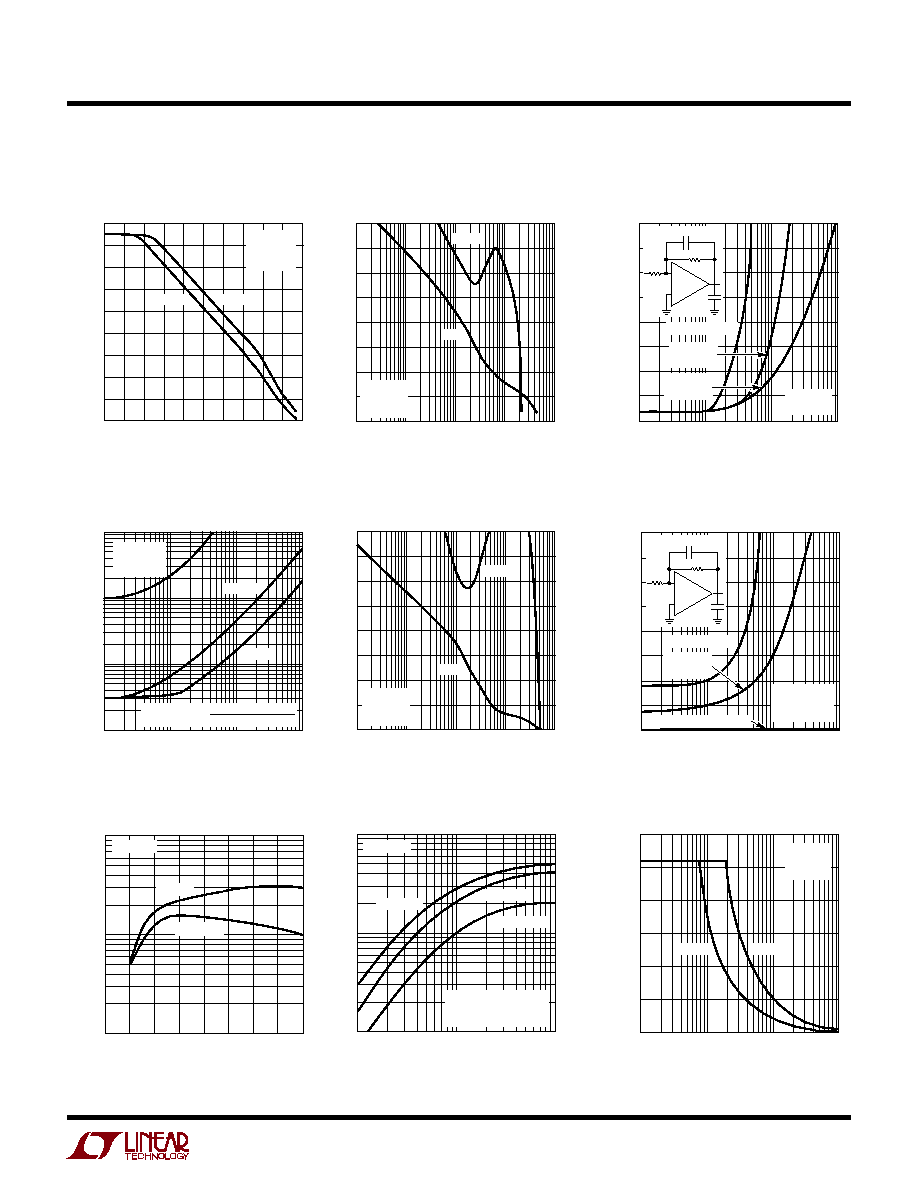
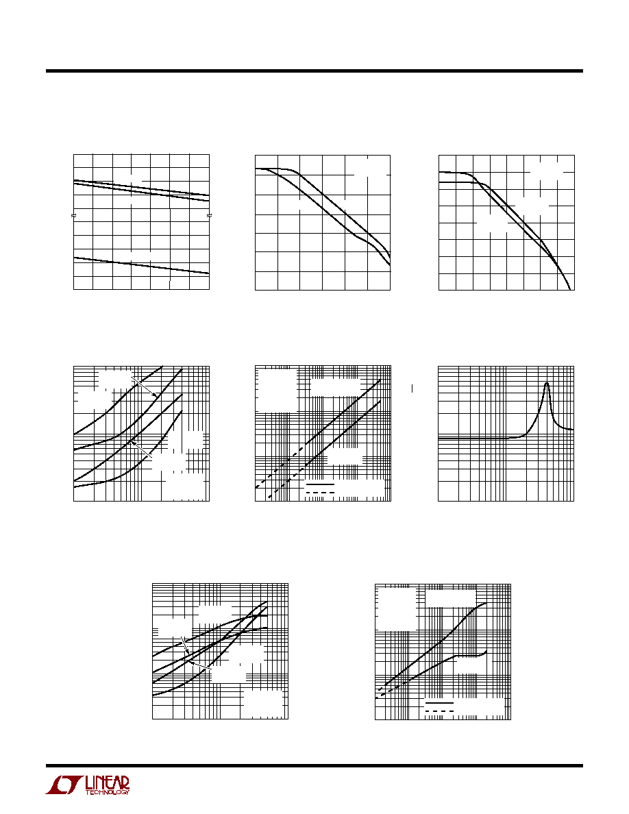
Gain Error vs Frequency
Closed-Loop Gain = 1000
LT1128
Gain Phase vs Frequency
LT1028
Gain, Phase vs Frequency
Voltage Gain vs Frequency
Voltage Gain vs Supply Voltage
Voltage Gain vs Load Resistance
FREQUENCY (Hz)
10k
5
PEAK-TO-PEAK OUTPUT VOLTAGE (V)
20
25
30
100k
1M
10M
LT1028/1128 ∑ TPC27
15
10
LT1128
LT1028
V
S
=
±
15V
T
A
= 25
∞
C
R
L
= 2k
Maximum Undistorted Output
vs Frequency
LT1128
Capacitance Load Handling
LT1028
Capacitance Load Handling
FREQUENCY (Hz)
0.01
≠20
VOLTAGE GAIN (dB)
160
LT1028/1128 ∑ TPC19
140
120
100
80
60
40
20
0
0.1
1
10 100 1k 10k 100k 1M 10M 100M
LT1128
LT1028
V
S
=
±
15V
T
A
= 25
∞
C
R
L
= 2k
CAPACITIVE LOAD (pF)
10
40
OVERSHOOT (%)
50
60
70
80
100
1000
10000
LT1028/1128 ∑ TPC 24
30
20
10
0
V
S
=
±
15V
T
A
= 25
∞
C
V
O
= 10mV
P-P
A
V
= ≠1, R
S
= 2k
≠
+
C
L
2k
30pF
R
S
A
V
= ≠10
R
S
= 200
A
V
= ≠100, R
S
= 20
FREQUENCY (Hz)
10
VOLTAGE GAIN (dB)
20
40
50
70
10k
1M
10M
100M
LT1028/1128 ∑ TPC23
≠10
100k
60
30
0
V
S
=
±
15V
T
A
= 25
∞
C
C
L
= 10pF
GAIN
PHASE
10
20
40
50
70
≠10
60
30
0
PHASE MARGIN (DEG)
FREQUENCY (Hz)
0.1
0.001
GAIN ERROR (%) 0.01
0.1
1
1
100
LT1028/1128 ∑ TPC22
LT1128
LT1028
TYPICAL
PRECISION
OP AMP
GAIN ERROR = CLOSED-LOOP GAIN
OPEN-LOOP GAIN
10
SUPPLY VOLTAGE (V)
±
5
1
10
100
±
10
±
15
LT`1028/1128 ∑ TPC25
VOLTAGE GAIN (V/
µ
V)
0
±
20
T
A
= 25
∞
C
R
L
= 2k
R
L
= 600
CAPACITIVE LOAD (pF)
10
40
OVERSHOOT (%)
50
60
70
80
100
1000
10000
LT1028/1128 ∑ TPC21
30
20
10
0
V
S
=
±
15V
T
A
= 25
∞
C
≠
+
C
L
2k
30pF
R
S
A
V
= ≠1, R
S
= 2k
A
V
= ≠100
R
S
= 20
A
V
= ≠10
R
S
= 200
FREQUENCY (Hz)
10
VOLTAGE GAIN (dB)
20
40
50
70
10k
1M
10M
100M
LT1028/1128 ∑ TPC20
≠10
100k
60
30
0
V
S
=
±
15V
T
A
= 25
∞
C
C
L
= 10pF
GAIN
PHASE
10
20
40
50
70
≠10
60
30
0
PHASE MARGIN (DEG)
LOAD RESISTANCE (k
)
0.1
1
VOLTAGE GAIN (V/
µ
V)
10
100
1
10
LT1028/1128 ∑ TPC26
V
S
=
±
15V
T
A
= ≠55
∞
C
T
A
= 25
∞
C
T
A
= 125
∞
C
I
LMAX
= 35mA AT ≠55
∞
C
= 27mA AT 25
∞
C
= 16mA AT 125
∞
C
8
LT1028/LT1128
C
C
HARA TERISTICS
U
W
A
TYPICAL PERFOR
CE
LT1128
Large-Signal Transient Response
FREQUENCY (Hz)
10
OUTPUT IMPEDANCE (
)
1
10
100
100k
LT1028/1128 ∑ TPC34
0.1
0.01
0.001
100
1k
10k
1M
I
O
= 1mA
V
S
=
±
15V
T
A
= 25
∞
C
LT1128
LT1028
LT1128
LT1028
A
V
= 1000
A
V
= 5
LT1028
Slew Rate, Gain-Bandwidth
Product Over Temperature
LT1128
Slew Rate, Gain-Bandwidth
Product Over Temperature
LT1028
Slew Rate, Gain-Bandwidth Product
vs Over-Compensation Capacitor
LT1128
Slew Rate, Gain-Bandwidth Product
vs Over-Compensation Capacitor
Closed-Loop Output Impedance
TEMPERATURE (∞C)
≠50
SLEW RATE (V/
µ
s) 16
17
18
25
75
LT1028/1128 ∑ TPC30
15
14
≠25
0
50
100
125
13
12
V
S
=
±
15V
70
80
90
60
50
40
30
GAIN-BANDWIDTH PRODUCT (f
O
= 20kHz), (MHz)
GBW
FALL
RISE
TEMPERATURE (
∞
C)
≠50
0
SLEW RATE (V/
µ
s)
1
3
4
5
0
50
100
9
LT1028/1128 ∑ TPC33
2
≠25
25
6
7
8
75
125
20
10
30
GAIN-BANDWIDTH PRODUCT (f
O
= 200kHz), (MHz)
FALL
RISE
GBW
OVER-COMPENSATION CAPACITOR (pF)
1
SLEW RATE (V/
µ
s) 10
1
100
1000
10000
LT1028/1128 ∑ TPC36
0.1
10
100
1k
10k
GAIN AT 20kHz
C
OC
FROM PIN 5 TO PIN 6
V
S
=
±
15V
T
A
= 25
∞
C
SLEW
GBW
100
10
OVER-COMPENSATION CAPACITOR (pF)
1
SLEW RATE (V/
µ
s) 10
1
100
1000
10000
LT1028/1128 ∑ TPC35
0.1
10
100
10
100
1
1k
GAIN AT 200kHz
GBW
SLEW RATE
OVER-COMPENSATION CAPACITOR (pF)
1
10
1
100
1000
10000
LT1028/1128 ∑ TPC35
0.1
10
100
10
100
1k
GBW
SLEW RATE
1
0V
A
V
= ≠1, R
S
= R
F
= 2k, C
F
= 30pF
2
µ
s/DIV
LT1128
Small-Signal Transient Response
0.2
µ
s/DIV
20mV/DIV
A
V
= ≠1, R
S
= R
F
= 2k
C
F
= 15pF, C
L
= 80pF
≠50mV
50mV
5V/DIV
10V
≠10V
0V
10V
≠50mV
50mV
≠10V
0.2
µ
s/DIV
1
µ
s/DIV
A
V
= ≠1, R
S
= R
F
= 2k, C
F
= 15pF
A
V
= 1, C
L
= 10pF
LT1028
Large-Signal Transient Response
LT1028
Small-Signal Transient Response
9
LT1028/LT1128
C
C
HARA TERISTICS
U
W
A
TYPICAL PERFOR
CE
LT1128
Total Harmonic Distortion vs
Closed-Loop Gain
Common Mode Limit Over
Temperature
LT1028
Total Harmonic Distortion vs
Frequency and Load Resistance
FREQUENCY (Hz)
10
80
100
120
10k
1M
LT1028/1128 ∑ TPC38
60
40
100
1k
100k
10M
20
0
COMMON MODE REJECTION RATIO (dB)
140
V
S
=
±
15V
T
A
= 25
∞
C
LT1128
LT1028
Common Mode Rejection Ratio
vs Frequency
Power Supply Rejection Ratio
vs Frequency
FREQUENCY (Hz)
10k
0.1
1.0
10
100k
1M
LT1028/1128 ∑ TPC42
NOISE VOLTAGE DENSITY (nV/
˜
Hz)
High Frequency Voltage Noise
vs Frequency
LT1028
Total Harmonic Distortion vs
Closed-Loop Gain
FREQUENCY (Hz)
0.1
POWER SUPPLY REJECTION RATIO (dB)
80
100
120
10M
LT1028/1128 ∑ TPC39
60
40
0
10
1k
100k
20
160
140
1M
1
100
10k
V
S
=
±
15V
T
A
= 25
∞
C
NEGATIVE
SUPPLY
POSITIVE
SUPPLY
LT1128
Total Harmonic Distortion vs
Frequency and Load Resistance
TEMPERATURE (
∞
C)
≠50
V
≠
COMMON MODE LIMIT (V)
REFERRED TO POWER SUPPLY
1
3
4
V
+
≠3
0
50
75
LT1028/1128 ∑ TPC37
2
≠2
≠1
≠4
≠25
25
100
125
V
S
=
±
5V
V
S
=
±
5V TO
±
15V
V
S
=
±
15V
CLOSED LOOP GAIN
0.001
TOTAL HARMONIC DISTORTION (%)
0.01
10
1k
10k
100k
LT1028/1128 ∑ TPC41
0.0001
100
0.1
V
O
= 20V
P-P
f = 1kHz
V
S
=
±
15V
T
A
= 25
∞
C
R
L
= 10k
NON-INVERTING
GAIN
INVERTING
GAIN
MEASURED
EXTRAPOLATED
CLOSED LOOP GAIN
0.001
TOTAL HARMONIC DISTORTION (%)
0.01
10
1k
10k
100k
LT1028/1128 ∑ TPC44
0.0001
100
0.1
V
O
= 20V
P-P
f = 1kHz
V
S
=
±
15V
T
A
= 25
∞
C
R
L
= 10k
NON-INVERTING
GAIN
INVERTING
GAIN
MEASURED
EXTRAPOLATED
FREQUENCY (kHz)
1
0.001
TOTAL HARMONIC DISTORTION (%)
0.01
0.1
10 100
LT1028/1128 ∑ TPC40
A
V
= 1000
R
L
= 600
A
V
= 1000
R
L
= 2k
A
V
= ≠1000
R
L
= 2k
V
O
= 20V
P-P
V
S
=
±
15V
T
A
= 25
∞
C
A
V
= 1000
R
L
= 600
FREQUENCY (kHz)
1.0
0.001
TOTAL HARMONIC DISTORTION (%)
0.1
1.0
10
100
LT1028/1128 ∑ TPC43
0.01
A
V
= 1000
R
L
= 600
A
V
= ≠1000
R
L
= 2k
V
O
= 20V
P-P
V
S
=
±
15V
T
A
= 25
∞
C
A
V
= 1000
R
L
= 600
A
V
= 1000
R
L
= 2k

10
LT1028/LT1128
largest term, as in the example above, and the LT1028/
LT1128's voltage noise becomes negligible. As R
eq
is
further increased, current noise becomes important. At
1kHz, when R
eq
is in excess of 20k, the current noise
component is larger than the resistor noise. The total noise
versus matched source resistance plot illustrates the
above calculations.
The plot also shows that current noise is more dominant
at low frequencies, such as 10Hz. This is because resistor
noise is flat with frequency, while the 1/f corner of current
noise is typically at 250Hz. At 10Hz when R
eq
> 1k, the
current noise term will exceed the resistor noise.
When the source resistance is unmatched, the total noise
versus unmatched source resistance plot should be con-
sulted. Note that total noise is lower at source resistances
below 1k because the resistor noise contribution is less.
When R
S
> 1k total noise is not improved, however. This
is because bias current cancellation is used to reduce
input bias current. The cancellation circuitry injects two
correlated current noise components into the two inputs.
With matched source resistors the injected current noise
creates a common-mode voltage noise and gets rejected
by the amplifier. With source resistance in one input only,
the cancellation noise is added to the amplifier's inherent
noise.
In summary, the LT1028/LT1128 are the optimum ampli-
fiers for noise performance, provided that the source
resistance is kept low. The following table depicts which
op amp manufactured by Linear Technology should be
used to minimize noise, as the source resistance is in-
creased beyond the LT1028/LT1128's level of usefulness.
≠
+
100
100k
100
LT1028
LT1128
1028/1128 AI01
U
S
A
O
PPLICATI
W
U
U
I FOR ATIO ≠ OISE
U
BEST OP AMP
AT LOW FREQ(10Hz)
WIDEBAND(1kHz)
SOURCE RESIS-
TANCE(
) (Note 1)
Best Op Amp for Lowest Total Noise vs Source Resistance
0 to 400
LT1028/LT1128
LT1028/LT1128
400 to 4k
LT1007/1037
LT1028/LT1128
4k to 40k
LT1001
LT1007/1037
40k to 500k
LT1012
LT1001
500k to 5M
LT1012 or LT1055
LT1012
>5M
LT1055
LT1055
Note 1: Source resistance is defined as matched or unmatched, e.g.,
R
S
= 1k means: 1k at each input, or 1k at one input and zero at the other.
Voltage Noise vs Current Noise
The LT1028/LT1128's less than 1nV/
Hz voltage noise is
three times better than the lowest voltage noise heretofore
available (on the LT1007/1037). A necessary condition for
such low voltage noise is operating the input transistors at
nearly 1mA of collector currents, because voltage noise is
inversely proportional to the square root of the collector
current. Current noise, however, is directly proportional to
the square root of the collector current. Consequently, the
LT1028/LT1128's current noise is significantly higher
than on most monolithic op amps.
Therefore, to realize truly low noise performance it is
important to understand the interaction between voltage
noise (e
n
), current noise (I
n
) and resistor noise (r
n
).
Total Noise vs Source Resistance
The total input referred noise of an op amp is given by
e
t
=
[
e
n
2
+ r
n
2
+ (I
n
R
eq
)
2
]
1/2
where R
eq
is the total equivalent source resistance at the
two inputs, and
r
n
=
4kTR
eq
= 0.13
R
eq
in nV/
Hz at 25
∞
C
As a numerical example, consider the total noise at 1kHz
of the gain 1000 amplifier shown below.
R
eq
= 100
+ 100
|| 100k
200
r
n
= 0.13
200 = 1.84nV
Hz
e
n
= 0.85nV
Hz
I
n
= 1.0pA/
Hz
e
t
=
[
0.85
2
+ 1.84
2
+ (1.0
◊
0.2)
2
]
1/2
= 2.04nV/
Hz
Output noise = 1000 e
t
= 2.04
µ
V/
Hz
At very low source resistance (R
eq
< 40
) voltage noise
dominates. As R
eq
is increased resistor noise becomes the
11
LT1028/LT1128
U
S
A
O
PPLICATI
W
U
U
I FOR ATIO
0.1Hz to 10Hz Noise Test Circuit
0.1Hz to 10Hz Peak-to-Peak Noise
Tester Frequency Response
FREQUENCY (Hz)
40
GAIN (dB)
60
70
90
100
0.01
1.0
10
100
LT1028/1128 ∑ AI03
30
0.1
50
80
≠
+
VOLTAGE GAIN = 50,000
* DEVICE UNDER TEST
NOTE ALL CAPACITOR VALUES ARE FOR
NONPOLARIZED CAPACITORS ONLY
100k
10
≠
+
2k
4.7
µ
F
0.1
µ
F
100k
24.3k
22
µ
F
2.2
µ
F
4.3k
110k
SCOPE
◊
1
R
IN
= 1M
0.1
µ
F
*
1028/1128 AI02
LT1001
≠ OISE
U
Noise Testing ≠ Voltage Noise
The LT1028/LT1128's RMS voltage noise density can be
accurately measured using the Quan Tech Noise Analyzer,
Model 5173 or an equivalent noise tester. Care should be
taken, however, to subtract the noise of the source resistor
used. Prefabricated test cards for the Model 5173 set the
device under test in a closed-loop gain of 31 with a 60
source resistor and a 1.8k feedback resistor. The noise of
this resistor combination is 0.13
58 = 1.0nV/
Hz. An
LT1028/LT1128 with 0.85nV/
Hz noise will read (0.85
2
+
1.0
2
)
1/2
= 1.31nV/
Hz. For better resolution, the resistors
should be replaced with a 10
source and 300
feedback
resistor. Even a 10
resistor will show an apparent noise
which is 8% to 10% too high.
The 0.1Hz to 10Hz peak-to-peak noise of the LT1028/
LT1128 is measured in the test circuit shown. The fre-
quency response of this noise tester indicates that the
0.1Hz corner is defined by only one zero. The test time to
measure 0.1Hz to 10Hz noise should not exceed 10
seconds, as this time limit acts as an additional zero to
eliminate noise contributions from the frequency band
below 0.1Hz.
Measuring the typical 35nV peak-to-peak noise perfor-
mance of the LT1028/LT1128 requires special test pre-
cautions:
(a) The device should be warmed up for at least five
minutes. As the op amp warms up, its offset voltage
changes typically 10
µ
V due to its chip temperature
increasing 30
∞
C to 40
∞
C from the moment the power
supplies are turned on. In the 10 second measure-
ment interval these temperature-induced effects can
easily exceed tens of nanovolts.
(b) For similar reasons, the device must be well shielded
from air current to eliminate the possibility of thermo-
electric effects in excess of a few nanovolts, which
would invalidate the measurements.
(c) Sudden motion in the vicinity of the device can also
"feedthrough" to increase the observed noise.
A noise-voltage density test is recommended when mea-
suring noise on a large number of units. A 10Hz noise-
voltage density measurement will correlate well with a
0.1Hz to 10Hz peak-to-peak noise reading since both
results are determined by the white noise and the location
of the 1/f corner frequency.
12
LT1028/LT1128
Noise Testing ≠ Current Noise
Current noise density (I
n
) is defined by the following
formula, and can be measured in the circuit shown:
If the Quan Tech Model 5173 is used, the noise reading is
input-referred, therefore the result should not be divided
by 31; the resistor noise should not be multiplied by 31.
100% Noise Testing
The 1kHz voltage and current noise is 100% tested on the
LT1028/LT1128 as part of automated testing; the approxi-
mate frequency response of the filters is shown. The limits
on the automated testing are established by extensive
correlation tests on units measured with the Quan Tech
Model 5173.
U
S
A
O
PPLICATI
W
U
U
I FOR ATIO
10Hz voltage noise density is sample tested on every lot.
Devices 100% tested at 10Hz are available on request for
an additional charge.
10Hz current noise is not tested on every lot but it can be
inferred from 100% testing at 1kHz. A look at the current
noise spectrum plot will substantiate this statement. The
only way 10Hz current noise can exceed the guaranteed
limits is if its 1/f corner is higher than 800Hz and/or its
white noise is high. If that is the case then the 1kHz test will
fail.
I
n
=
[e
no
2
≠ (31
◊
18.4nV/
Hz)
2
]
1/2
20k
◊
31
≠
+
e
no
1.8k
60
LT1028
LT1128
10k
10k
1028/1128 AI04
≠ OISE
U
FREQUENCY (Hz)
100
≠50
NOISE FILTER LOSS (dB)
≠10
0
10
1k
10k
100k
LT1028/1128 ∑ AI05
≠20
≠40
≠30
CURRENT
NOISE
VOLTAGE
NOISE
U
S
A
O
PPLICATI
W
U
U
I FOR ATIO
General
The LT1028/LT1128 series devices may be inserted di-
rectly into OP-07, OP-27, OP-37, LT1007 and LT1037
sockets with or without removal of external nulling com-
ponents. In addition, the LT1028/LT1128 may be fitted to
5534 sockets with the removal of external compensation
components.
Offset Voltage Adjustment
The input offset voltage of the LT1028/LT1128 and its drift
with temperature, are permanently trimmed at wafer test-
ing to a low level. However, if further adjustment of V
OS
is
necessary, the use of a 1k nulling potentiometer will not
degrade drift with temperature. Trimming to a value other
Automated Tester Noise Filter
≠
+
6
1k
INPUT
LT1028
LT1128
1028/1128 AI06
7
8
1
2
3
4
OUTPUT
≠15V
15V
than zero creates a drift of (V
OS
/300)
µ
V/
∞
C, e.g., if V
OS
is
adjusted to 300
µ
V, the change in drift will be 1
µ
V/
∞
C.
The adjustment range with a 1k pot is approximately
±
1.1mV.
Offset Voltage and Drift
Thermocouple effects, caused by temperature gradients
across dissimilar metals at the contacts to the input
13
LT1028/LT1128
Frequency Response
The LT1028's Gain, Phase vs Frequency plot indicates that
the device is stable in closed-loop gains greater than +2 or
≠1 because phase margin is about 50
∞
at an open-loop
gain of 6dB. In the voltage follower configuration phase
margin seems inadequate. This is indeed true when the
output is shorted to the inverting input and the noninvert-
ing input is driven from a 50
source impedance. How-
ever, when feedback is through a parallel R-C network
(provided C
F
< 68pF), the LT1028 will be stable because of
interaction between the input resistance and capacitance
and the feedback network. Larger source resistance at the
noninverting input has a similar effect. The following
voltage follower configurations are stable:
Another configuration which requires unity-gain stability
is shown below. When C
F
is large enough to effectively
short the output to the input at 15MHz, oscillations can
occur. The insertion of R
S2
500
will prevent the
LT1028 from oscillating. When R
S1
500
, the additional
noise contribution due to the presence of R
S2
will be
minimal. When R
S1
100
, R
S2
is not necessary, be-
cause R
S1
represents a heavy load on the output through
the C
F
short. When 100
< R
S1
< 500
, R
S2
should match
R
S1
. For example, R
S1
= R
S2
= 300
will be stable. The
noise increase due to R
S2
is 40%.
U
S
A
O
PPLICATI
W
U
U
I FOR ATIO
terminals, can exceed the inherent drift of the amplifier
unless proper care is exercised. Air currents should be
minimized, package leads should be short, the two input
leads should be close together and maintained at the same
temperature.
The circuit shown to measure offset voltage is also used
as the burn-in configuration for the LT1028/LT1128.
1028/1128 AI09
≠
+
33pF
2k
LT1028
50
≠
+
LT1028
50
500
1028/1128 AI10
C1
R1
R
S1
R
S2
LT1028
≠
+
Unity-Gain Buffer Applications (LT1128 Only)
When R
F
100
and the input is driven with a fast, large-
signal pulse (>1V), the output waveform will look as
shown in the pulsed operation diagram.
During the fast feedthrough-like portion of the output, the
input protection diodes effectively short the output to the
input and a current, limited only by the output short-circuit
protection, will be drawn by the signal generator. With R
F
500
, the output is capable of handling the current
requirements (I
L
20mA at 10V) and the amplifier stays
in its active mode and a smooth transition will occur.
As with all operational amplifiers when R
F
> 2k, a pole will
be created with R
F
and the amplifier's input capacitance,
creating additional phase shift and reducing the phase
margin. A small capacitor (20pF to 50pF) in parallel with R
F
will eliminate this problem.
Test Circuit for Offset Voltage
and Offset Voltage Drift with Temperature
≠
+
≠15V
10k*
200
*
LT1028
LT1128
1028/1128 AI08
10k*
V
O
= 100V
OS
* RESISTORS MUST HAVE LOW
THERMOELECTRIC POTENTIAL
V
O
6
7
2
4
3
15V
≠
+
R
F
1028/1128 AI07
OUTPUT
6V/
µ
s
14
LT1028/LT1128
U
S
A
O
PPLICATI
W
U
U
I FOR ATIO
If C
F
is only used to cut noise bandwidth, a similar effect
can be achieved using the over-compensation terminal.
The Gain, Phase plot also shows that phase margin is
about 45
∞
at gain of 10 (20dB). The following configura-
tion has a high (
70%) overshoot without the 10pF
capacitor because of additional phase shift caused by the
feedback resistor ≠ input capacitance pole. The presence
of the 10pF capacitor cancels this pole and reduces
overshoot to 5%.
Over-Compensation
The LT1028/LT1128 are equipped with a frequency over-
compensation terminal (Pin 5). A capacitor connected
between Pin 5 and the output will reduce noise bandwidth.
Details are shown on the Slew Rate, Gain-Bandwidth
Product vs Over-Compensation Capacitor plot. An addi-
tional benefit is increased capacitive load handling capa-
bility.
1028/1128 AI11
10pF
10k
50
1.1k
≠
+
LT1028
Strain Gauge Signal Conditioner with Bridge Excitation
Low Noise Voltage Regulator
1028/1128 TA05
1
µ
F
REFERENCE
OUTPUT
≠
+
LT1128
30.1k*
49.9
*
15V
330
10k
ZERO
TRIM
5.0V
301k*
LT1021-5
0V TO 10V
OUTPUT
3
2
7
6
4
350
BRIDGE
≠15V
15V
15V
LT1028
≠
+
3
2
7
6
4
≠15V
LT1028
≠
+
3
2
7
6
4
≠15V
5k
GAIN
TRIM
330
*RN60C FILM RESISTORS
THE LT1028's NOISE CONTRIBUTION IS NEGLIGIBLE
COMPARED TO THE BRIDGE NOISE.
1028/1128 TA04
10
2k
20V OUTPUT
≠
+
LT1028
2.3k
PROVIDES PRE-REG
AND CURRENT
LIMITING
10
+
28V
121
2k
330
1000pF
1k
28V
LT317A
LT1021-10
2N6387
TYPICAL APPLICATIO S
U
15
LT1028/LT1128
Paralleling Amplifiers to Reduce Voltage Noise
Tape Head Amplifier
1028/1128 TA07
0.1
µ
F
10
≠
+
LT1028
OUTPUT
499
TAPE HEAD
INPUT
6
31.6k
2
3
ALL RESISTORS METAL FILM
Phono Preamplifier
1028/1128 TA06
0.1
µ
F
10
≠15V
10k
≠
+
LT1028
OUTPUT
787
0.33
µ
F
100pF
47k
MAG PHONO
INPUT
4
6
7
15V
2
3
ALL RESISTORS METAL FILM
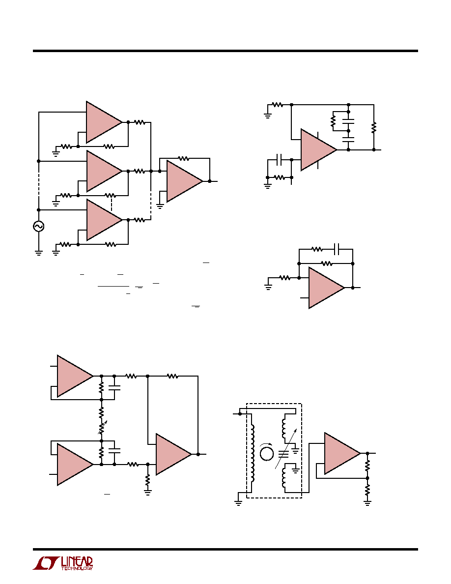
Low Noise, Wide Bandwidth Instrumentation Amplifier
Gyro Pick-Off Amplifier
1028/1128 TA08
10
≠
+
LT1028
OUTPUT
820
+INPUT
68pF
10k
50
68pF
820
≠
+
LT1028
≠INPUT
≠
+
LT1028
300
300
10k
GAIN = 1000, BANDWIDTH = 1MHz
INPUT REFERRED NOISE = 1.5nV/
Hz AT 1kHz
WIDEBAND NOISE ≠DC to 1MHz = 3
µ
V
RMS
IF BW LIMITED TO DC TO 100kHz = 0.55
µ
V
RMS
1028/1128 TA09
100
OUTPUT TO SYNC
DEMODULATOR
1k
≠
+
LT1028
SINE
DRIVE
∑
GYRO TYPICAL≠
NORTHROP CORP.
GR-F5AH7-5B
1028/1128 TA03
≠
+
1.5k
A1
LT1028
470
OUTPUT
≠
+
7.5
4.7k
≠
+
1.5k
470
7.5
≠
+
1.5k
470
7.5
A2
LT1028
An
LT1028
LT1028
OUTPUT NOISE
n
◊
200
2
µ
V
5
1. ASSUME VOLTAGE NOISE OF LT1028 AND 7.5
SOURCE RESISTOR = 0.9nV/
Hz.
2. GAIN WITH n LT1028s IN PARALLEL = n
◊
200.
3. OUTPUT NOISE =
n
◊
200
◊
0.9nV/
Hz.
4. INPUT REFERRED NOISE = = nV/
Hz.
5. NOISE CURRENT AT INPUT INCREASES
n TIMES.
6. IF n = 5, GAIN = 1000, BANDWIDTH = 1MHz, RMS NOISE, DC TO 1MHz = = 0.9
µ
V.
0.9
n
TYPICAL APPLICATIO S
U
16
LT1028/LT1128
Super Low Distortion Variable Sine Wave Oscillator
1028/1128 TA10
≠
+
LT1028
C2
0.047
R2
R1
C1
0.047
2k
20
20
2k
10pF
5.6k
15
µ
F
+
22k
10k
≠
+
LT1055
1V
RMS
OUTPUT
1.5kHz TO 15kHz
WHERE R1C1 = R2C2
f =
1
2
RC
(
)
MOUNT 1N4148s
IN CLOSE PROXIMITY
TRIM FOR
LOWEST
DISTORTION
100k
10k
20k
2N4338
560
2.4k
4.7k
LT1004-1.2V
15V
<0.0018% DISTORTION AND NOISE.
MEASUREMENT LIMITED BY RESOLUTION OF
HP339A DISTORTION ANALYZER
1028/1128 TA11
≠
+
LT1052
10
0.1
30k
10k
15V
7
6
4
2
3
8
1
≠15V
0.1
0.01
15V
68
≠
+
LT1028
130
1
7
8
4
≠15V
INPUT
OUTPUT
1N758
1N758
100k
2
3
Chopper-Stabilized Amplifier
TYPICAL APPLICATIO S
U
17
LT1028/LT1128
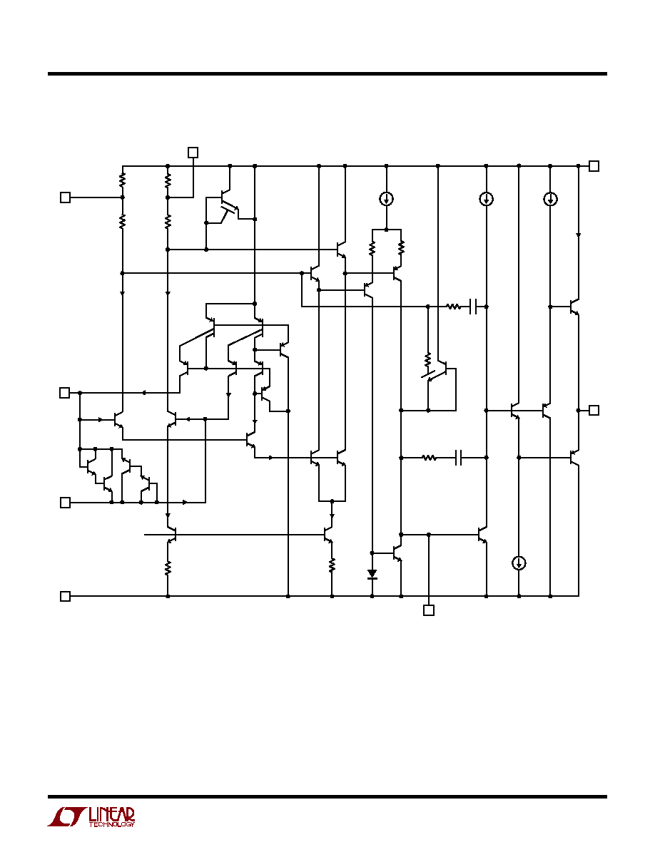
S
W
A
W
CHE
TI
I
C D AGRA
1.5
µ
A
1
NULL
R5
130
R6
130
R1
3k
R2
3k
3
8
NULL
Q4
C1
257pF
900
µ
A
900
µ
A
Q6
Q5
Q9
Q8
Q7
Q2
4.5
µ
A
4.5
µ
A
1.5
µ
A
Q13
Q14
Q1
4.5
µ
A
NON-
INVERTING
INPUT
0
1.8mA
Q3
BIAS
2
INVERTING
INPUT
4
V
≠
R7
80
Q11
Q10
Q12
300
µ
A
Q15
Q21
5
OVER-
COMP
Q23
600
µ
A
R12
240
C4
35pF
Q22
R11
100
C3
250pF
Q19
Q18
Q16
Q17
R11
400
R10
400
1.1mA
2.3mA
400
µ
A
V
+
7
R10
500
C2
Q26
Q25
Q24
6
OUTPUT
Q27
1028/1128 TA13
4.5
µ
A
3
1
3
1
Q20
R8
480
500
µ
A
C2 = 50pF for LT1028
C2 = 275pF for LT1128
18
LT1028/LT1128
S8 Package
8-Lead Plastic Small Outline (Narrow .150 Inch)
(Reference LTC DWG # 05-08-1610)
N8 Package
8-Lead PDIP (Narrow .300 Inch)
(Reference LTC DWG # 05-08-1510)
J8 Package
8-Lead CERDIP (Narrow .300 Inch, Hermetic)
(Reference LTC DWG # 05-08-1110)
PACKAGE DESCRIPTIO
U
J8 1298
0.014 ≠ 0.026
(0.360 ≠ 0.660)
0.200
(5.080)
MAX
0.015 ≠ 0.060
(0.381 ≠ 1.524)
0.125
3.175
MIN
0.100
(2.54)
BSC
0.300 BSC
(0.762 BSC)
0.008 ≠ 0.018
(0.203 ≠ 0.457)
0
∞
≠ 15
∞
0.005
(0.127)
MIN
0.405
(10.287)
MAX
0.220 ≠ 0.310
(5.588 ≠ 7.874)
1
2
3
4
8
7
6
5
0.025
(0.635)
RAD TYP
0.045 ≠ 0.068
(1.143 ≠ 1.727)
FULL LEAD
OPTION
0.023 ≠ 0.045
(0.584 ≠ 1.143)
HALF LEAD
OPTION
CORNER LEADS OPTION
(4 PLCS)
0.045 ≠ 0.065
(1.143 ≠ 1.651)
NOTE: LEAD DIMENSIONS APPLY TO SOLDER DIP/PLATE
OR TIN PLATE LEADS
N8 1098
0.100
(2.54)
BSC
0.065
(1.651)
TYP
0.045 ≠ 0.065
(1.143 ≠ 1.651)
0.130
±
0.005
(3.302
±
0.127)
0.020
(0.508)
MIN
0.018
±
0.003
(0.457
±
0.076)
0.125
(3.175)
MIN
1
2
3
4
8
7
6
5
0.255
±
0.015*
(6.477
±
0.381)
0.400*
(10.160)
MAX
0.009 ≠ 0.015
(0.229 ≠ 0.381)
0.300 ≠ 0.325
(7.620 ≠ 8.255)
0.325
+0.035
≠0.015
+0.889
≠0.381
8.255
(
)
*THESE DIMENSIONS DO NOT INCLUDE MOLD FLASH OR PROTRUSIONS.
MOLD FLASH OR PROTRUSIONS SHALL NOT EXCEED 0.010 INCH (0.254mm)
0.016 ≠ 0.050
(0.406 ≠ 1.270)
0.010 ≠ 0.020
(0.254 ≠ 0.508)
◊
45
∞
0
∞
≠ 8
∞
TYP
0.008 ≠ 0.010
(0.203 ≠ 0.254)
SO8 1298
0.053 ≠ 0.069
(1.346 ≠ 1.752)
0.014 ≠ 0.019
(0.355 ≠ 0.483)
TYP
0.004 ≠ 0.010
(0.101 ≠ 0.254)
0.050
(1.270)
BSC
1
2
3
4
0.150 ≠ 0.157**
(3.810 ≠ 3.988)
8
7
6
5
0.189 ≠ 0.197*
(4.801 ≠ 5.004)
0.228 ≠ 0.244
(5.791 ≠ 6.197)
DIMENSION DOES NOT INCLUDE MOLD FLASH. MOLD FLASH
SHALL NOT EXCEED 0.006" (0.152mm) PER SIDE
DIMENSION DOES NOT INCLUDE INTERLEAD FLASH. INTERLEAD
FLASH SHALL NOT EXCEED 0.010" (0.254mm) PER SIDE
*
**
OBSOLETE PACKAGE
19
LT1028/LT1128
S Package
16-Lead Plastic Small Outline (Narrow .150 Inch)
(Reference LTC DWG # 05-08-1610)
H Package
3-Lead TO-39 Metal Can
(Reference LTC DWG # 05-08-1330)
PACKAGE DESCRIPTIO
U
Information furnished by Linear Technology Corporation is believed to be accurate and reliable.
However, no responsibility is assumed for its use. Linear Technology Corporation makes no represen-
tation that the interconnection of its circuits as described herein will not infringe on existing patent rights.
0.050
(1.270)
MAX
0.016 ≠ 0.021**
(0.406 ≠ 0.533)
0.010 ≠ 0.045*
(0.254 ≠ 1.143)
SEATING
PLANE
0.040
(1.016)
MAX
0.165 ≠ 0.185
(4.191 ≠ 4.699)
GAUGE
PLANE
REFERENCE
PLANE
0.500 ≠ 0.750
(12.700 ≠ 19.050)
0.305 ≠ 0.335
(7.747 ≠ 8.509)
0.335 ≠ 0.370
(8.509 ≠ 9.398)
DIA
0.230
(5.842)
TYP
0.027 ≠ 0.045
(0.686 ≠ 1.143)
0.028 ≠ 0.034
(0.711 ≠ 0.864)
0.110 ≠ 0.160
(2.794 ≠ 4.064)
INSULATING
STANDOFF
45
∞
TYP
H8 (TO-5) 0.230 PCD 1197
LEAD DIAMETER IS UNCONTROLLED BETWEEN THE REFERENCE PLANE
AND 0.045" BELOW THE REFERENCE PLANE
FOR SOLDER DIP LEAD FINISH, LEAD DIAMETER IS
0.016 ≠ 0.024
(0.406 ≠ 0.610)
*
**
PIN 1
0.016 ≠ 0.050
(0.406 ≠ 1.270)
0.010 ≠ 0.020
(0.254 ≠ 0.508)
◊
45
∞
0
∞
≠ 8
∞
TYP
0.008 ≠ 0.010
(0.203 ≠ 0.254)
1
2
3
4
5
6
7
8
0.150 ≠ 0.157**
(3.810 ≠ 3.988)
16
15
14
13
0.386 ≠ 0.394*
(9.804 ≠ 10.008)
0.228 ≠ 0.244
(5.791 ≠ 6.197)
12
11
10
9
S16 1098
0.053 ≠ 0.069
(1.346 ≠ 1.752)
0.014 ≠ 0.019
(0.355 ≠ 0.483)
TYP
0.004 ≠ 0.010
(0.101 ≠ 0.254)
0.050
(1.270)
BSC
DIMENSION DOES NOT INCLUDE MOLD FLASH. MOLD FLASH
SHALL NOT EXCEED 0.006" (0.152mm) PER SIDE
DIMENSION DOES NOT INCLUDE INTERLEAD FLASH. INTERLEAD
FLASH SHALL NOT EXCEED 0.010" (0.254mm) PER SIDE
*
**
OBSOLETE PACKAGE
20
LT1028/LT1128
Linear Technology Corporation
1630 McCarthy Blvd., Milpitas, CA 95035-7417
(408) 432-1900
q
FAX: (408) 434-0507
q
www.linear.com
©
LINEAR TECHNOLOGY CORPORATION 1992
1028fa LT/CP 0901 1.5K REV A ∑ PRINTED IN USA
RELATED PARTS
PART NUMBER
DESCRIPTION
COMMENTS
LT1806/LT1807
325MHz, 3.5nV/
Hz Single and Dual Op Amps
Slew Rate = 140V/
µ
s, Low Distortion at 5MHz: ≠80dBc
Low Noise Infrared Detector
1028/1128 TA12
10
1M
1k
10k
5V
≠
+
LT1028
7
6
4
2
3
8
≠5V
1000
µ
F
DC OUT
5V
39
33
+
267
10
+
+
OPTICAL
CHOPPER
WHEEL
IR
RADIATION
PHOTO-
ELECTRIC
PICK-OFF
INFRA RED ASSOCIATES, INC.
HgCdTe IR DETECTOR
13
AT 77
∞
K
1/4 LTC1043
30pF
100
µ
F
100
µ
F
13
14
16
10k*
10k*
SYNCHRONOUS
DEMODULATOR
≠
+
LT1012
7
4
2
3
≠5V
6
5V
1
8
12
≠
+
LM301A
7
4
2
3
≠5V
6
5V
1
8
U
TYPICAL APPLICATIO