 | –≠–ª–µ–∫—Ç—Ä–æ–Ω–Ω—ã–π –∫–æ–º–ø–æ–Ω–µ–Ω—Ç: LT1031DC | –°–∫–∞—á–∞—Ç—å:  PDF PDF  ZIP ZIP |
1
LT1031/LH0070
1031fa
Pin Compatible with LH0070 and AD581*
Ultralow Drift--5ppm/∞C Max Slope
Trimmed Output Voltage
Operates in Series or Shunt Mode
Output Sinks and Sources in Series Mode
Very Low Noise < 1ppm
P-P
0.1Hz to 10Hz
> 100dB Ripple Rejection
Minimum Input Voltage of 11V
The LT
Æ
1031 is a precision 10V reference with ultralow
drift and noise, extremely good long term stability, and
almost total immunity to input voltage variations. The
reference output will both source and sink up to 10mA and
can be used as a shunt regulator (two terminal Zener) with
the same precision characteristics as the three terminal
connection. Special care has been taken to minimize
thermal regulation effects and temperature induced
hysteresis.
The LT1031 reference is based on a buried Zener diode
structure which eliminates noise and stability problems
associated with surface breakdown devices. Further, a
subsurface Zener exhibits better temperature drift and
time stability than even the best band-gap references.
Unique circuit design makes the LT1031 the first three
terminal IC reference to offer ultralow drift without the
use of high power on-chip heaters. Output voltage is
pretrimmed to 0.05% accuracy.
The LT1031 can be used as a plug-in replacement for
the AD581 and LH0070*, with improved electrical and
thermal performance.
A-to-D and D-to-A Converters
Precision Regulators
Digital Voltmeters
lnertial Navigation Systems
Precision Scales
Portable Reference Standard
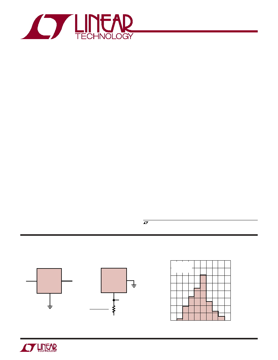
Basic Positive and
Negative Connections
Precision 10V Reference
Distribution of Output Accuracy
FEATURES
APPLICATIO S
U
DESCRIPTIO
U
*See LH0070 Electrical Characteristics table and AD581 cross reference guide.
, LTC and LT are registered trademarks of Linear Technology Corporation.
V
OUT
I
LOAD
+ 1.5mA
≠ V
OUT
≠ V
IN
V
IN
≠ V
OUT
V
IN
LT1031
LT1031
IN
OUT
R1 =
R1
OUT
GND
GND
LT1031 ∑ TA01
OUTPUT ACCURACY (%)
≠0.10
PERCENT OF UNITS (%)
15
20
25
0
0.06
LT1031 ∑ TA02
10
5
0
≠0.06
≠0.02
0.02
30
35
40
0.10
T
A
= 25∞C
DISTRIBUTION
FROM 5 RUNS
TYPICAL APPLICATIO
U
2
LT1031/LH0070
1031fa
Input Voltage ........................................................... 40V
Input-Output Voltage Differential ............................. 35V
Output to Ground Voltage
(Shunt Mode Current Limit) ................................. 16V
Trim Pin to Ground Voltage
Positive ................................................. Equal to V
OUT
Negative ............................................................. ≠ 20V
Output Short-Circuit Duration
V
IN
= 35V ......................................................... 10 sec
V
IN
20V ..................................................... Indefinite
Operating Temperature Range
LT1031M .......................................... ≠ 55∞C to 125∞C
LT1031C .................................................. 0∞C to 70∞C
Lead Temperature (Soldering, 10 sec).................. 300∞C
LT1031
SYMBOL
PARAMETER
CONDITIONS
MIN
TYP
MAX
UNITS
V
R
Output Voltage (Note 2)
LT1031B
9.995
10.000
10.005
V
LT1031C
9.990
10.000
10.010
V
LT1031D
9.980
10.000
10.020
V
V
R
Output Voltage Temperature
T
MIN
T
J
T
MAX
T
Coefficient (Note 3)
LT1031B
3
5
ppm/∞C
LT1031C
6
15
ppm/∞C
LT1031D
10
25
ppm/∞C
V
R
Line Regulation (Note 4)
11.5V V
IN
14.5V
1
4
ppm/V
V
IN
6
ppm/V
4.5V V
IN
40V
0.5
2
ppm/V
4
ppm/V
V
R
Load Regulation (Sourcing Current)
0 I
OUT
10mA
12
25
ppm/mA
I
O
(Note 4)
40
ppm/mA
V
R
Load Regulation (Shunt Mode)
1.7mA I
SHUNT
10mA
50
100
ppm/mA
I
O
(Notes 4, 5)
150
ppm/mA
I
Q
Series Mode Supply Current
1.2
1.7
mA
2.0
mA
I
MIN
Shunt Mode Minimum Current
V
IN
is Open
1.1
1.5
mA
1.7
mA
Output Short-Circuit Current
11V V
IN
35V
30
mA
Minimum Input Voltage (Note 7)
l
OUT
1mA
10.8
11.0
V
e
n
Output Voltage Noise
0.1Hz f 10Hz
6
µV
P-P
0.1Hz f 10Hz
11
µV
RMS
V
R
Long Term Stability of
t = 1000 Hrs
15
ppm
Time
Output Voltage
Non-Cumulative
Temperature Hysteresis of Output
T = 50∞C
5
ppm
ABSOLUTE AXI U RATI GS
W
W
W
U
Consult LTC Marketing for parts specified with wider operating temperature ranges.
(Note 1)
PACKAGE/ORDER I FOR ATIO
U
U
W
(LT1031) The
denotes the specifications which apply over the full operating
temperature range, otherwise specifications are at T
A
= 25∞C. V
IN
= 15V, I
OUT
= 0, Mil or Comm version, unless noted.
ELECTRICAL CHARACTERISTICS
BOTTOM VIEW
INPUT
1
2
3
OUTPUT
GROUND
H PACKAGE
3-LEAD TO-39 METAL CAN
ORDER PART
NUMBER
LH0070-0H
LH0070-1H
LH0070-2H
LT1031BMH
LT1031DMH
LT1031BCH
LT1031CCH
LT1031DCH
LT1031 ∑ POI01
T
JMAX
= 150
∞
C,
JA
= 150
∞
C/W,
JC
= 45
∞
C/W (LH0070)
T
JMAX
= 150
∞
C,
JA
= 150
∞
C/W,
JC
= 45
∞
C/W (LT1031M)
T
JMAX
= 85
∞
C,
JA
= 150
∞
C/W,
JC
= 45
∞
C/W (LT1031C)
3
LT1031/LH0070
1031fa
(LH0070) The
denotes the specifications which apply over the full
operating temperature range. V
IN
= 15V, R
L
= 10k, ≠55∞C T
A
125∞C, unless noted.
ELECTRICAL CHARACTERISTICS
Note 1: Absolute Maximum Ratings are those values beyond which the life
of a device may be impaired.
Note 2: Output voltage is measured immediately after turn-on. Changes
due to chip warm-up are typically less than 0.005%.
Note 3: Temperature coefficient is measured by dividing the change in
output voltage over the temperature range by the change in temperature.
Separate tests are done for hot and cold: T
MIN
to 25∞C and 25∞C to T
MAX
.
Incremental slope is also measured at 25
∞
C. For LT1031BMH, the
5ppm/∞C drift specification is for ≠ 25∞C to 85∞C. Drift over the full ≠ 55∞C
to 125∞C range is guaranteed to 7ppm/∞C.
Note 4: Line and load regulation are measured on a pulse basis. Output
changes due to die temperature change must be taken into account
separately. Package thermal resistance is 150∞C/W.
Note 5: Shunt mode regulation is measured with the input open. With the
input connected, shunt mode current can be reduced to 0mA. Load
regulation will remain the same.
Note 6: Temperature drift is guaranteed from ≠25∞C to 85∞C on LH0070.
Note 7: See curve for guaranteed minimum V
IN
versus I
OUT
.
Note 8: Guaranteed by design.
LH0070
SYMBOL
PARAMETER
CONDITIONS
MIN
TYP
MAX
UNITS
V
R
Output Voltage
T
A
= 25∞C
10.000
V
V
R
Output Accuracy
T
A
= 25∞C
≠ 0, ≠1
± 0.03
± 0.1
%
≠ 2
± 0.02
± 0.05
%
V
R
Output Accuracy
T
A
= ≠55∞C, 125∞C
≠ 0, ≠1
0.3
%
≠ 2
0.2
%
V
R
Output Voltage Change
Note 6
T
with Temperature
≠ 0
± 0.2
%
≠ 1
± 0.02
± 0.1
%
≠ 2
± 0.01
± 0.04
%
V
R
Line Regulation
13V V
IN
33V, T
A
= 25∞C
V
IN
≠ 0, ≠1
0.006
0.1
%
≠ 2
0.006
0.03
%
Input Voltage Range
11.4
40
V
V
R
Load Regulation
0mA l
OUT
5mA
0.01
0.03
%
I
O
I
Q
Quiescent Current
13V V
IN
33V
1.2
5
mA
l
Q
Change in Quiescent Current
V
IN
= 20V from 13V TO 33V
0.1
1.5
mA
V
IN
e
n
Output Noise Voltage
6
µV
P-P
Ripple Rejection
f = 120Hz
0.001
%/V
P-P
r
O
Output Resistance
0.2
0.6
V
Z
Long Term Stability
T
A
= 25∞C (Note 8)
Time
≠ 0, ≠1
± 0.2
%/Yr
≠ 2
± 0.05
%/Yr
4
LT1031/LH0070
1031fa
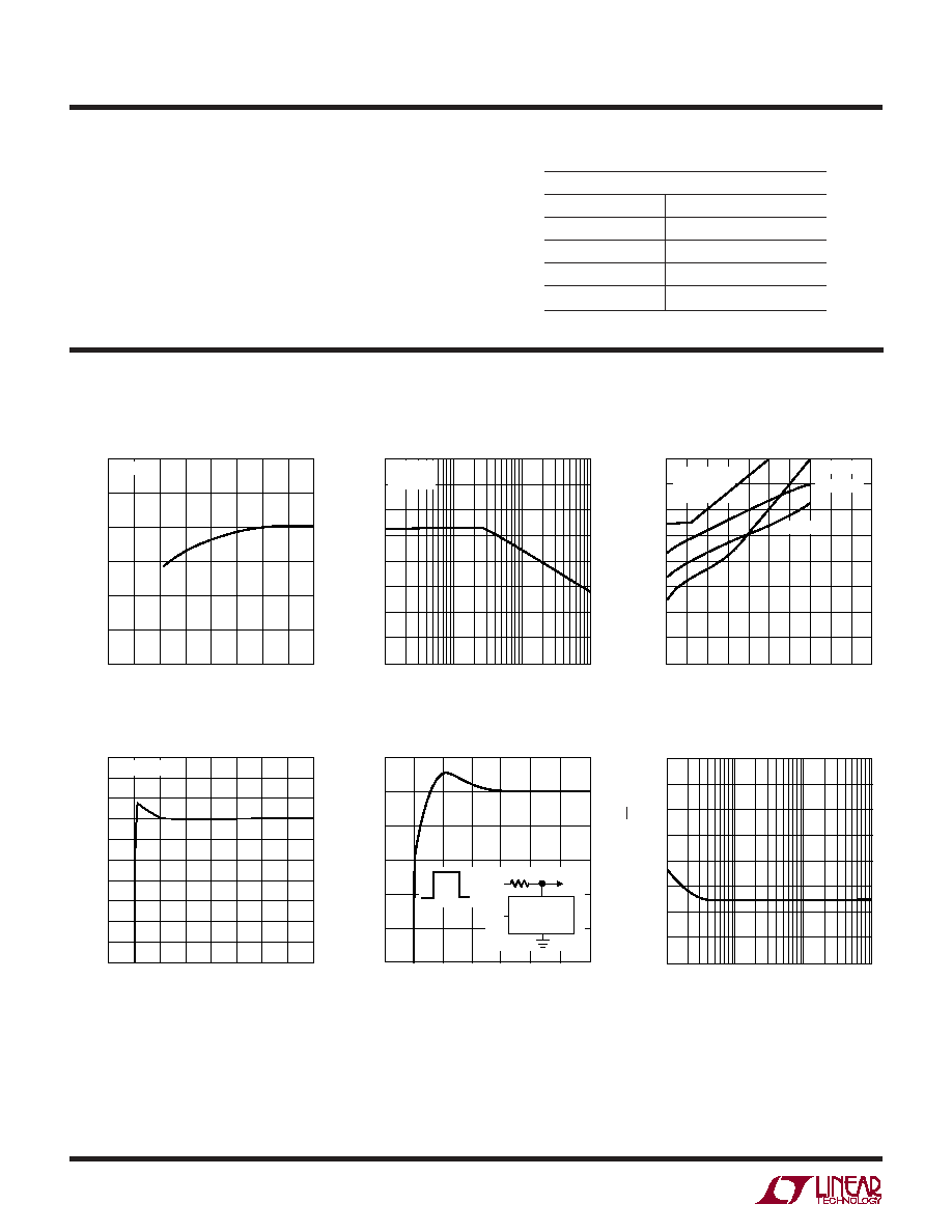
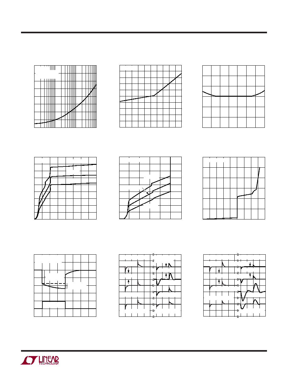
TYPICAL PERFOR A CE CHARACTERISTICS
U
W
The following cross reference guide may be used to select
LT1031 grades which meet or exceed output voltage,
temperature drift, load and line regulation, and output
current specifications of the AD581 reference. Parameters
such as noise, hysteresis, and long term stability will be
significantly better for all LT1031 grades compared to the
AD581.
Ripple Rejection
Minimum Input Voltage
Ripple Rejection
INPUT VOLTAGE (V)
0
85
REJECTION (dB)
90
95
100
105
10
20
30
40
LT1031 ∑ TPC01
110
115
5
15
25
35
f = 150Hz
OUTPUT CURRENT (mA)
0
INPUT VOLTAGE (V)
11.6
11.4
11.2
11.0
10.8
10.6
10.4
10.2
10.0
16
LT1031 ∑ TPC03
4
8
12
20
14
2
6
10
18
GUARANTEED
CURVE-ALL
TEMPS
T
J
= 25∞C
T
J
= 125∞C
T
J
= ≠55∞C
LT1031 ∑ TPC02
FREQUENCY (Hz)
10
90
REJECTION (dB)
110
130
100
1k
10k
70
80
100
120
60
50
V
IN
= 15V
C
OUT
= 0
Start-Up (Series Mode)
Start-Up (Shunt Mode)
Output Voltage Noise Spectrum
TIME (µs)
3
OUTPUT VOLTAGE (V)
4
6
7
8
13
10
2
6
8
LT1031 ∑ TPC04
5
11
12
9
0
4
10
12
14
V
IN
= 0 TO 12V
LT1031 ∑ TPC06
FREQUENCY (Hz)
10
200
NOISE VOLTAGE (nV/
Hz) 300
400
100
1k
10k
100
150
250
350
50
0
CROSS REFERE
N
CE
U
TIME (µs)
OUTPUT VOLTAGE (V)
9
10
11
4
8
8
7
0
2
6
10
12
6
5
LT1031 ∑ TPC05
NC
0V
≠12V
GND
IN
V
OUT
OUT
1k
CROSS REFERENCE GUIDE/LT1031 TO AD581
AD581J
order LT1031DCH
AD581K
order LT1031CCH
AD581L
order LT1031BCH
A0581S
order LT1031DMH
A0581U
order LT1031BMH
5
LT1031/LH0070
1031fa
Output Voltage Noise
Load Regulation
TYPICAL PERFOR A CE CHARACTERISTICS
U
W
Output Voltage Temperature
LT1031 ∑ TPC07
BANDWIDTH (Hz)
10
8
RMS NOISE (
µ
V)
12
16
100
1k
10k
4
6
10
14
2
0
C
OUT
= 0
FILTER = 1 POLE
f
LOW
= 0.1Hz
SOURCING
OUTPUT CURRENT (mA)
SINKING
≠10
OUTPUT CHANGE (mV)
1
3
2
0
≠2
≠4
5
4
6
≠1
≠3
≠5
≠6
≠8
≠2
≠4
2
4
8
0
10
LT1031 ∑ TPC08
V
IN
= 12V
TEMPERATURE (∞C)
≠50
OUTPUT VOLTAGE (V)
10.002
10.004
10.006
25
75
10.000
9.998
≠25
0
50
100
125
9.996
9.994
LT1031 ∑ TPC09
Input Supply Current
Shunt Mode Current Limit
Shunt Characteristics
INPUT VOLTAGE (V)
0
5
INPUT CURRENT (mA)
1.0
1.2
1.4
35
40
0.8
0.6
0.2
0
10
15
20
25
30
0.4
1.8
1.6
LT1031 ∑ TPC10
I
OUT
= 0
T
J
= 125∞C
T
J
= ≠55∞C
T
J
= 25∞C
OUTPUT TO GROUND VOLTAGE (V)
0
0
CURRENT INTO OUTPUT (mA)
0.2
0.6
0.8
1.0
8
1.8
0.4
4
2
6
10
12
1.2
1.4
1.6
LT1031 ∑ TPC11
INPUT PIN OPEN
T
J
= 125∞C
T
J
= ≠55∞C
T
J
= 25∞C
OUTPUT VOLTAGE (V)
0
0
CURRENT INTO OUTPUT (mA)
10
30
40
50
4
8
10
18
20
2
6
12
14
16
60
LT1031 ∑ TPC12
INPUT PIN IS OPEN
Thermal Regulation
Load Transient Response
C
LOAD
= 0
Load Transient Response
C
LOAD
= 1000pF
TIME (
µ
s)
OUTPUT VOLTAGE CHANGE
4
2
0
6
4
0
2
6
8
8
LT1031 ∑ TPC15
NOTE VERTICAL SCALE CHANGE
BETWEEN SOURCING AND SINKING
I
SINK
= 2 TO 10mA
I
SOURCE
= 0
I
SINK
= 1.4mA
I
SINK
= 1.2mA
I
SOURCE
= 100
µ
Ap-p
I
SOURCE
= 0.5mA
I
SOURCE
= 2 TO 10mA
I
SINK
= 100
µ
Ap-p
5mV
20mV
I
SINK
= 0.8mA
TIME (ms)
*INDEPENDENT OF TEMPERATURE COEFFICIENT
OUTPUT CHANGE (mV)
≠1.0
0
140
20
≠20
60
100
0
40
80
120
≠1.5
≠0.5
LT1031 ∑ TPC13
I
LOAD
= 10mA
V
IN
= 30V
POWER = 200mW
LOAD
REGULATION
THERMAL*
REGULATION
TIME (
µ
s)
OUTPUT VOLTAGE CHANGE
7
1
0
≠2
3
2
5
6
8
4
9
LT1031 ∑ TPC14
NOTE VERTICAL SCALE CHANGE
BETWEEN SOURCING AND SINKING
I
SINK
= 2 TO 10mA
I
SOURCE
= 0
I
SINK
= 1.0mA
I
SINK
= 0.8mA
I
SOURCE
= 100
µ
Ap-p
I
SOURCE
= 0.2mA
I
SOURCE
= 2 TO 10mA
I
SINK
= 0.6mA
I
SINK
= 100
µ
Ap-p
10mV
50mV