 | –≠–ª–µ–∫—Ç—Ä–æ–Ω–Ω—ã–π –∫–æ–º–ø–æ–Ω–µ–Ω—Ç: LT1054 | –°–∫–∞—á–∞—Ç—å:  PDF PDF  ZIP ZIP |

1
LT1054/LT1054L
Switched-Capacitor Voltage
Converter with Regulator
S
FEATURE
D
U
ESCRIPTIO
s
Available in Space Saving SO-8 Package
s
Output Current: 100mA (LT1054)
125mA (LT1054L)
s
Low Loss: 1.1V at 100mA
s
Operating Range:3.5V to 15V (LT1054)
3.5V to 7V (LT1054L)
s
Reference and Error Amplifier for Regulation
s
External Shutdown
s
External Oscillator Synchronization
s
Can Be Paralleled
s
Pin Compatible with the LTC
Æ
1044/LTC7660
The LT
Æ
1054 is a monolithic, bipolar, switched-capacitor
voltage converter and regulator. The LT1054 provides
higher output current than previously available converters
with significantly lower voltage losses. An adaptive switch
driver scheme optimizes efficiency over a wide range of
output currents. Total voltage loss at 100mA output current
is typically 1.1V. This holds true over the full supply voltage
range of 3.5V to 15V. Quiescent current is typically 2.5mA.
The LT1054 also provides regulation, a feature not previ-
ously available in switched-capacitor voltage converters.
By adding an external resistive divider a regulated output
can be obtained. This output will be regulated against
changes in both input voltage and output current. The
LT1054 can also be shut down by grounding the feedback
pin. Supply current in shutdown is less than 100
µ
A.
The internal oscillator of the LT1054 runs at a nominal
frequency of 25kHz. The oscillator pin can be used to adjust
the switching frequency or to externally synchronize the
LT1054.
The LT1054 is pin compatible with previous converters
such the LTC1044/LTC7660.
OUTPUT CURRENT (mA)
0
VOLTAGE LOSS (V)
1
2
50
1054 TA01∑
0
25
75
100
125
T
J
= 125
∞
C
T
J
= 25
∞
C
T
J
= ≠55
∞
C
LT1054
LT1054L
3.5V
V
IN
15V (LT1054)
3.5V
V
IN
7V (LT1054L)
C
IN
= C
OUT
= 100
µ
F
INDICATES GUARANTEED
TEST POINT
, LTC and LT are registered trademarks of Linear Technology Corporation.
LT1054/LT1054L Voltage Loss
s
Voltage Inverter
s
Voltage Regulator
s
Negative Voltage Doubler
s
Positive Voltage Doubler
U
S
A
O
PPLICATI
REFERENCE
OSC
DRIVE
DRIVE
DRIVE
DRIVE
OSC
CAP
≠
GND
CAP
+
FEEDBACK/
SHUTDOWN
≠
+
R
R
*EXTERNAL CAPACITORS
2.5V
6
1
4
3
≠V
OUT
LT1054 ∑ BD
5
2
8
7
Q
Q
V
REF
C
IN
*
V
IN
C
OUT
*
+
+
BLOCK DIAGRA
M
W
2
LT1054/LT1054L
A
U
G
W
A
W
U
W
A
R
BSOLUTE
XI
TI
S
Supply Voltage (Note 2)
LT1054 ................................................................ 16V
LT1054L ................................................................ 7V
Input Voltage
Pin 1 ................................................. 0V
V
PIN1
V
+
Pin 3 (S Package) ............................. 0V
V
PIN3
V
+
Pin 7 ............................................. 0V
V
PIN7
V
REF
Pin 13 (S Package) ...................... 0V
V
PIN13
V
REF
Operating Junction Temperature Range
LT1054C/LT1054LC ............................. 0
∞
C to 100
∞
C
LT1054I ........................................... ≠ 40
∞
C to 100
∞
C
LT1054M ......................................... ≠ 55
∞
C to 125
∞
C
Maximum Junction Temperature (Note 3)
LT1054C/LT1054LC ........................................ 125
∞
C
LT1054I ............................................................ 125
∞
C
LT1054M ......................................................... 150
∞
C
Storage Temperature Range
H, J8, N8 and S8 Packages ................ ≠55
∞
C to 150
∞
C
S Package ........................................ ≠ 65
∞
C to 150
∞
C
Lead Temperature (Soldering, 10 sec)................. 300
∞
C
W
U
U
PACKAGE/ORDER I FOR ATIO
ORDER PART
NUMBER
LT1054CH
LT1054MH
T
JMAX
= 150
∞
C,
JA
= 150
∞
C,
JC
= 45
∞
C/W
TOP VIEW
OSC
V
+
FB/SHDN
V
REF
V
OUT
GND
CAP
≠
CASE
IS
V
OUT
CAP
+
8
7
6
5
3
2
1
4
H PACKAGE
8-LEAD TO-5 METAL CAN
T
JMAX
= 125
∞
C,
JA
= 120
∞
C/W
ORDER PART
NUMBER
T
JMAX
= 125
∞
C,
JA
= 150
∞
C/W
1
2
3
4
8
7
6
5
TOP VIEW
FB/SHDN
CAP
+
GND
CAP
≠
V
+
OSC
V
REF
V
OUT
N8 PACKAGE
8-LEAD PLASTIC DIP
J8 PACKAGE
8-LEAD CERAMIC DIP
T
JMAX
= 150
∞
C,
JA
= 100
∞
C/ W (J8)
T
JMAX
= 125
∞
C,
JA
= 130
∞
C/ W (N8)
1
2
3
4
8
7
6
5
TOP VIEW
V
+
OSC
V
REF
V
OUT
FB/SHDN
CAP
+
GND
CAP
≠
S8 PACKAGE
8-LEAD PLASTIC SO
SEE REGULATION AND CAPACITOR SELECTION SECTIONS
IN THE APPLICATIONS INFORMATION FOR IMPORTANT
INFORMATION ON THE S8 DEVICE
(Note 6)
ORDER PART
NUMBER
LT1054CS8
LT1054LCS8
S8 PART
MARKING
1054
1054L
(Note 1)
ORDER PART
NUMBER
LT1054CSW
LT1054ISW
LT1054CJ8
LT1054CN8
LT1054IN8
LT1054MJ8
1
2
3
4
5
6
7
8
TOP VIEW
SW PACKAGE
16-LEAD PLASTIC SO
16
15
14
13
12
11
10
9
NC
NC
FB/SHDN
CAP
+
GND
CAP
≠
NC
NC
NC
NC
V
+
OSC
V
REF
V
OUT
NC
NC
OT RECO
M
M
E
DED
FOR EW
DESIG
S
U
U
U
U
WW

3
LT1054/LT1054L
ELECTRICAL C
C
HARA TERISTICS
PARAMETER
CONDITIONS
MIN
TYP
MAX
UNITS
Supply Current
I
LOAD
= 0mA
LT1054:
V
IN
= 3.5V
q
2.5
4.0
mA
V
IN
= 15V
q
3.0
5.0
mA
LT1054L: V
IN
= 3.5V
q
2.5
4.0
mA
V
IN
= 7V
q
3.0
5.0
mA
Supply Voltage Range
LT1054
q
3.5
15
V
LT1054L
q
3.5
7
V
Voltage Loss (V
IN
≠
V
OUT
)
C
IN
= C
OUT
= 100
µ
F Tantalum (Note 4)
I
OUT
= 10mA
q
0.35
0.55
V
I
OUT
= 100mA
q
1.10
1.60
V
I
OUT
= 125mA (LT1054L)
q
1.35
1.75
V
Output Resistance
I
OUT
= 10mA to 100mA (Note 5)
q
10
15
Oscillator Frequency
LT1054: 3.5V
V
IN
15V
q
15
25
35
kHz
LT1054L: 3.5V
V
IN
7V
q
15
25
35
kHz
Reference Voltage
I
REF
= 60
µ
A, T
J
= 25
∞
C
2.35
2.50
2.65
V
q
2.25
2.75
V
Regulated Voltage
V
IN
= 7V, T
J
= 25
∞
C, R
L
= 500
(Note 6)
≠ 4.70
≠ 5.00
≠ 5.20
V
Line Regulation
LT1054: 7V
V
IN
12V, R
L
= 500
(Note 6)
q
5
25
mV
Load Regulation
V
IN
= 7V, 100
R
L
500
(Note 6)
q
10
50
mV
Maximum Switch Current
300
mA
Supply Current in Shutdown
V
PIN1
= 0V
q
100
200
µ
A
(Note 7)
Note 5: Output resistance is defined as the slope of the curve, (
V
OUT
vs
I
OUT
), for output currents of 10mA to 100mA. This represents the linear
portion of the curve. The incremental slope of the curve will be higher at
currents < 10mA due to the characteristics of the switch transistors.
Note 6: All regulation specifications are for a device connected as a
positive-to-negative converter/regulator with R1 = 20k, R2 = 102.5k,
C1 = 0.002
µ
F, (C1 = 0.05
µ
F S package) C
IN
= 10
µ
F tantalum,
C
OUT
= 100
µ
F tantalum.
Note 7: The S8 package uses a different die than the H, J8, N8 and S
packages. The S8 device will meet all the existing data sheet parameters.
See Regulation and Capacitor Selection in the Applications Information
section for differences in application requirements.
The
q
denotes specifications which apply over the full operating
temperature range.
Note 1: Absolute Maximum Ratings are those values beyond which the life
of a device may be impaired.
Note 2: The absolute maximum supply voltage rating of 16V is for
unregulated circuits using LT1054. For regulation mode circuits using
LT1054 with V
OUT
15V at Pin 5 (Pin 11 on S package), this rating may
be increased to 20V. The absolute maximum supply voltage for LT1054L
is 7V.
Note 3: The devices are guaranteed by design to be functional up to the
absolute maximum junction temperature.
Note 4: For voltage loss tests, the device is connected as a voltage
inverter, with pins 1, 6, and 7 (3, 12, and 13 S package) unconnected.
The voltage losses may be higher in other configurations.
4
LT1054/LT1054L
C
C
HARA TERISTICS
U
W
A
TYPICAL PERFOR
CE
Shutdown Threshold
TEMPERATURE (∞C)
≠50
≠70
15
FREQUENCY (kHz)
25
35
0
50
75
LT1054 ∑ TPC03
≠25
25
100 125
V
IN
= 15V
V
IN
= 3.5V
INPUT VOLTAGE (V)
0
0
SUPPLY CURRENT (mA)
1
2
3
4
5
I
L
= 0
5
10
15
LT1054 ∑ TPC02
Supply Current in Shutdown
INPUT VOLTAGE (V)
0
0
QUIESCENT CURRENT (
µ
A)
20
40
60
80
120
5
10
15
LT1054 ∑ TPC04
100
V
PIN1
= 0V
OUTPUT CURRENT (mA)
0
0
AVERAGE INPUT CURRENT (mA)
20
60
80
100
140
LT1050 ∑ TPC05
40
120
40
100
20
60
80
INPUT CAPACITANCE (
µ
F)
0
0
VOLTAGE LOSS (V)
0.2
0.6
0.8
1.0
1.4
10
50
70
LT1054 ∑ TPC06
0.4
1.2
40
90 100
20 30
60
80
INVERTER CONFIGURATION
C
OUT
= 100
µ
F TANTALUM
f
OSC
= 25kHz
I
OUT
= 100mA
I
OUT
= 50mA
I
OUT
= 10mA
OSCILLATOR FREQUENCY (kHz)
1
0
VOLTAGE LOSS (V)
1
2
10
100
LT1054 ∑ TPC07
INVERTER CONFIGURATION
C
IN
= 10
µ
F TANTALUM
C
OUT
= 100
µ
F TANTALUM
I
OUT
= 100mA
I
OUT
= 50mA
I
OUT
= 10mA
OSCILLATOR FREQUENCY (kHz)
1
0
VOLTAGE LOSS (V)
1
2
10
100
LT1054 ∑ TPC08
INVERTER CONFIGURATION
C
IN
= 100
µ
F TANTALUM
C
OUT
= 100
µ
F TANTALUM
I
OUT
= 100mA
I
OUT
= 50mA
I
OUT
= 10mA
TEMPERATURE (∞C)
≠ 50
SHUTDOWN THRESHOLD (V)
0.4
0.5
0.6
25
75
LT1054 ∑ TPC01
0.3
0.2
≠ 25
0
50
100
125
0.1
0
V
PIN1
Supply Current
Oscillator Frequency
Average Input Current
Output Voltage Loss
Output Voltage Loss
Output Voltage Loss
5
LT1054/LT1054L
C
C
HARA TERISTICS
U
W
A
TYPICAL PERFOR
CE
TEMPERATURE (∞C)
≠50
≠100
REFERENCE VOLTAGE CHANGE (mV) ≠80
≠40
≠20
0
100
40
0
50
75
LT1054 ∑ TPC10
≠60
60
80
20
≠25
25
100
125
V
REF
AT 0 = 2.500V
TEMPERATURE (∞C)
≠50
≠12.6
OUTPUT VOLTAGE (V)
≠12.4
≠12.0
≠11.8
≠11.6
≠4.7
≠5.0
0
50
75
LT1054 ∑ TPC09
≠12.2
≠4.9
≠4.8
≠5.1
≠25
25
100
125
Regulated Output Voltage
Reference Voltage Temperature
Coefficient
PI
N
FU
N
CTIO
N
S
U
U
U
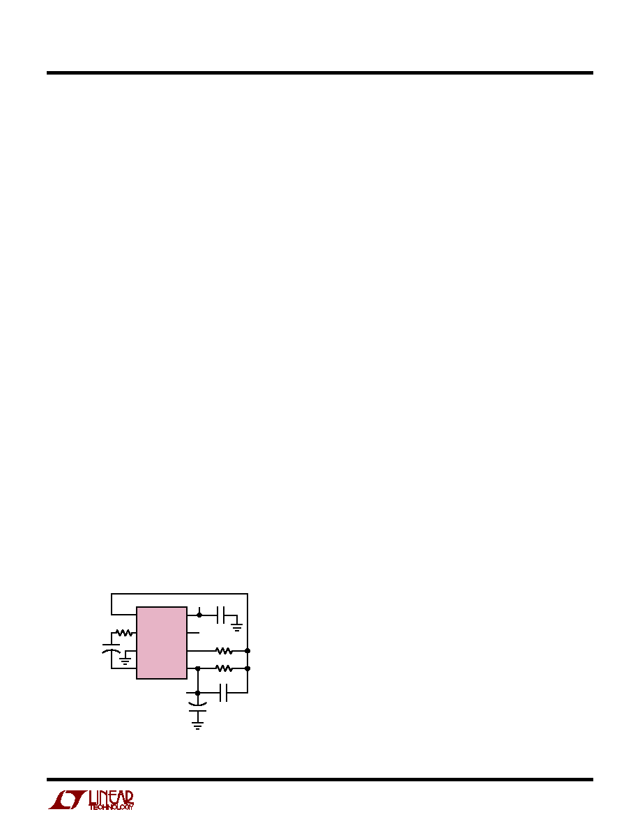
Pin 1 is also the inverting input of the LT1054's error
amplifier and as such can be used to obtain a regulated
output voltage.
CAP
+
/CAP
≠
(Pin 2/Pin 4): Pin 2, the positive side of the
input capacitor (C
IN
), is alternately driven between V
+
and
ground. When driven to V
+
, Pin 2 sources current from V
+
.
When driven to ground Pin 2 sinks current to ground. Pin
4, the negative side of the input capacitor, is driven alter-
nately between ground the V
OUT
. When driven to ground,
Pin 4 sinks current to ground. When driven to V
OUT
Pin 4
sources current from C
OUT
. In all cases current flow in the
switches is unidirectional as should be expected using
bipolar switches.
V
OUT
(Pin 5): In addition to being the output pin this pin is
also tied to the substrate of the device. Special care must
be taken in LT1054 circuits to avoid pulling this pin
positive with respect to any of the other pins. Pulling Pin
5 positive with respect to Pin 3 (GND) will forward bias the
substrate diode which will prevent the device from starting.
This condition can occur when the output load driven by the
LT1054 is referred to its positive supply (or to some other
positive voltage). Note that most op amps present just such
a load since their supply currents flow from their V
+
terminals to their V
≠
terminals. To prevent start-up prob-
lems with this type of load an external transistor must be
added as shown in Figure 1. This will prevent V
OUT
(Pin 5)
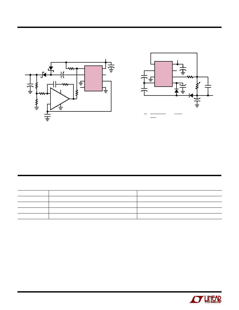
FB/SHDN (Pin 1): Feedback/Shutdown Pin. This pin has
two functions. Pulling Pin 1 below the shutdown threshold
(
0.45V) puts the device into shutdown. In shutdown the
reference/regulator is turned off and switching stops. The
switches are set such that both C
IN
and C
OUT
are dis-
charged through the output load. Quiescent current in
shutdown drops to approximately 100
µ
A (see Typical
Performance Characteristics). Any open-collector gate can
be used to put the LT1054 into shutdown. For normal
(unregulated) operation the device will start back up when
the external gate is shut off. In LT1054 circuits that use the
regulation feature, the external resistor divider can provide
enough pull-down to keep the device in shutdown until the
output capacitor (C
OUT
) has fully discharged. For most
applications where the LT1054 would be run intermittently,
this does not present a problem because the discharge time
of the output capacitor will be short compared to the off-
time of the device. In applications where the device has to
start up before the output capacitor (C
OUT
) has fully dis-
charged, a restart pulse must be applied to Pin 1 of the
LT1054. Using the circuit of Figure 5, the restart signal can
be either a pulse (t
p
> 100
µ
s) or a logic high. Diode coupling
the restart signal into Pin 1 will allow the output voltage to
come up and regulate without overshoot. The resistor
divider R3/R4 in Figure 5 should be chosen to provide a
signal level at pin 1 of 0.7V to 1.1V.
6
LT1054/LT1054L
PI
N
FU
N
CTIO
N
S
U
U
U
from being pulled above the ground pin (Pin 3) during
start-up. Any small, general purpose transistor such as
2N2222 or 2N2219 can be used. R
X
should be chosen to
provide enough base drive to the external transistor so that
it is saturated under nominal output voltage and maximum
output current conditions. In some cases an N-channel
enhancement mode MOSFET can be used in place of the
transistor.
R
X
(
|
V
OUT
|
)
I
OUT
≠
+
LOAD
C
IN
C
OUT
LT1054 ∑ F01
I
L
V
+
R
X
LT1054
FB/SHDN
CAP
+
GND
CAP
≠
V
+
OSC
V
REF
V
OUT
I
Q
I
OUT
+
+
V
REF
(Pin 6): Reference Output. This pin provides a 2.5V
reference point for use in LT1054-based regulator circuits.
The temperature coefficient of the reference voltage has
been adjusted so that the temperature coefficient of the
regulated output voltage is close to zero. This requires the
reference output to have a positive temperature coefficient
as can be seen in the typical performance curves. This
nonzero drift is necessary to offset a drift term inherent in
the internal reference divider and comparator network tied
to the feedback pin. The overall result of these drift terms
is a regulated output which has a slight positive tempera-
ture coefficient at output voltages below 5V and a slight
negative TC at output voltages above 5V. Reference output
current should be limited, for regulator feedback networks,
to approximately 60
µ
A. The reference pin will draw
100
µ
A when shorted to ground and will not affect the
internal reference/regulator, so that this pin can also be
used as a pull-up for LT1054 circuits that require synchro-
nization.
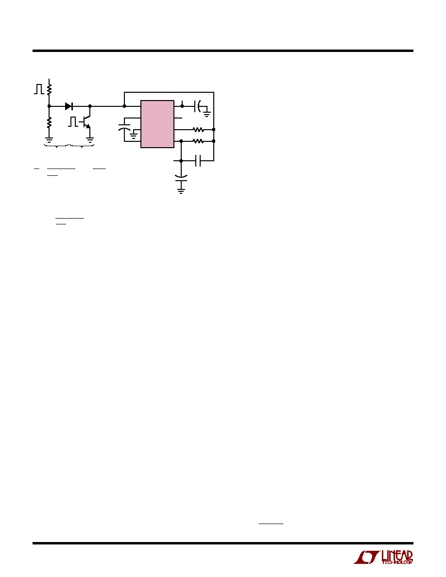
OSC (Pin 7): Oscillator Pin. This pin can be used to raise or
lower the oscillator frequency or to synchronize the device
to an external clock. Internally Pin 7 is connected to the
oscillator timing capacitor (C
t
150pF) which is alternately
charged and discharged by current sources of
±
7
µ
A so that
the duty cycle is
50%. The LT1054 oscillator is designed
to run in the frequency band where switching losses are
minimized. However the frequency can be raised, lowered,
or synchronized to an external system clock if necessary.
The frequency can be lowered by adding an external
capacitor (C1, Figure 2) from Pin 7 to ground. This will
increase the charge and discharge times which lowers the
oscillator frequency. The frequency can be increased by
adding an external capacitor (C2, Figure 2, in the range of
5pF to 20pF) from Pin 2 to Pin 7. This capacitor will couple
charge into C
T
at the switch transitions, which will shorten
the charge and discharge time, raising the oscillator fre-
quency. Synchronization can be accomplished by adding
an external resistive pull-up from Pin 7 to the reference pin
(Pin 6). A 20k pull-up is recommended. An open collector
gate or an NPN transistor can then be used to drive the
oscillator pin at the external clock frequency as shown in
Figure 2. Pulling up Pin 7 to an external voltage is
not recommended. For circuits that require both fre-
quency synchronization and regulation, an external refer-
ence can be used as the reference point for the top of the
R1/R2 divider allowing Pin 6 to be used as a pull-up point
for Pin 7.
Figure 1
V
+
(Pin 8): Input Supply. The LT1054 alternately charges
C
IN
to the input voltage when C
IN
is switched in parallel with
the input supply and then transfers charge to C
OUT
when
C
IN
is switched in parallel with C
OUT
. Switching occurs at
V
IN
C
OUT
C
IN
C2
C1
LT1054 ∑ F02
LT1054
FB/SHDN
CAP
+
GND
CAP
≠
V
+
OSC
V
REF
V
OUT
+
+
Figure 2
7
LT1054/LT1054L
the oscillator frequency. During the time that C
IN
is charg-
ing, the peak supply current will be approximately equal to
2.2 times the output current. During the time that C
IN
is
delivering charge to C
OUT
the supply current drops to
approximately 0.2 times the output current. An input
supply bypass capacitor will supply part of the peak input
current drawn by the LT1054 and average out the current
drawn from the supply. A minimum input supply bypass
capacitor of 2
µ
F, preferably tantalum or some other low
ESR type is recommended. A larger capacitor may be
desirable in some cases, for example, when the actual input
supply is connected to the LT1054 through long leads, or
when the pulse current drawn by the LT1054 might affect
other circuitry through supply coupling.
PI
N
FU
N
CTIO
N
S
U
U
U
APPLICATIO
N
S I
N
FOR
M
ATIO
N
W
U
U
U
Theory of Operation
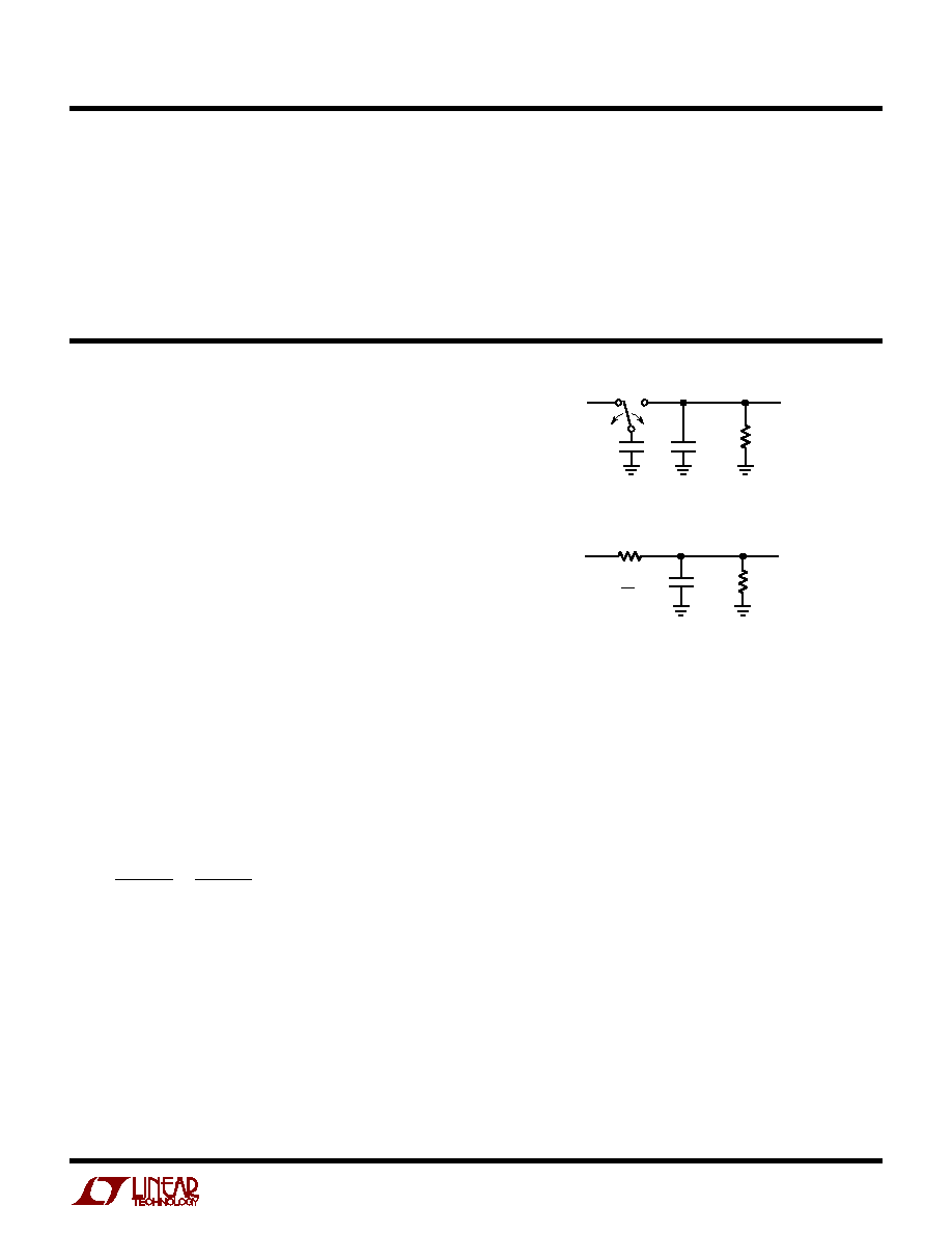
To understand the theory of operation of the LT1054, a
review of a basic switched-capacitor building block is
helpful.
In Figure 3 when the switch is in the left position, capacitor
C1 will charge to voltage V1. The total charge on C1 will be
q1 = C1V1. The switch then moves to the right, discharging
C1 to voltage V2. After this discharge time the charge on C1
is q2 = C1V2. Note that charge has been transferred from
the source V1 to the output V2. The amount of charge
transferred is:
q = q1 ≠ q2 = C1(V1 ≠ V2)
If the switch is cycled f times per second, the charge
transfer per unit time (i.e., current) is:
I = (f)(
q) = (f)[C1(V1 ≠ V2)]
To obtain an equivalent resistance for the switched-capaci-
tor network we can rewrite this equation in terms of voltage
and impedance equivalence:
I =
=
V1 ≠ V2
(1/fC1)
V1 ≠ V2
R
EQUIV
A new variable R
EQUIV
is defined such that R
EQUIV
= 1/fC1.
Thus the equivalent circuit for the switched-capacitor
network is as shown in Figure 4. The LT1054 has the same
switching action as the basic switched-capacitor building
block. Even though this simplification doesn't include finite
switch on-resistance and output voltage ripple, it provides
an intuitive feel for how the device works.
These simplified circuits explain voltage loss as a function
of frequency (see Typical Performance Characteristics). As
frequency is decreased, the output impedance will eventu-
f
C1
C2
R
L
V2
LT1054 ∑ F03
V1
Figure 3. Switched-Capacitor Building Block
C2
R
L
R
EQUIV
R
EQUIV
=
V2
LT1054 ∑ F04
V1
1
fC1
Figure 4. Switched-Capacitor Equivalent Circuit
ally be dominated by the 1/fC1 term and voltage losses will
rise.
Note that losses also rise as frequency increases. This is
caused by internal switching losses which occur due to
some finite charge being lost on each switching cycle. This
charge loss per-unit-cycle, when multiplied by the switch-
ing frequency, becomes a current loss. At high frequency
this loss becomes significant and voltage losses again rise.
The oscillator of the LT1054 is designed to run in the
frequency band where voltage losses are at a minimum.
Regulation
The error amplifier of the LT1054 servos the drive to the
PNP switch to control the voltage across the input capaci-
tor (C
IN
) which in turn will determine the output voltage.
Using the reference and error amplifier of the LT1054, an
external resistive divider is all that is needed to set the
regulated output voltage. Figure 5 shows the basic regu-
lator configuration and the formula for calculating the
appropriate resistor values. R1 should be chosen to be
8
LT1054/LT1054L
APPLICATIO
N
S I
N
FOR
M
ATIO
N
W
U
U
U
voltage. For the basic configuration,
|
V
OUT
|
referred to the
ground pin of the LT1054 must be less than the total of the
supply voltage minus the voltage loss due to the switches.
The voltage loss versus output current due to the switches
can be found in Typical Performance Characteristics. Other
configurations such as the negative doubler can provide
higher output voltages at reduced output currents (see
Typical Applications).
Capacitor Selection
For unregulated circuits the nominal values of C
IN
and C
OUT
should be equal. For regulated circuits see the section on
Regulation. While the exact values of C
IN
and C
OUT
are
noncritical, good quality, low ESR capacitors such as solid
tantalum are necessary to minimize voltage losses at high
currents. For C
IN
the effect of the ESR of the capacitor will
be multiplied by four due to the fact that switch currents are
approximately two times higher than output current and
losses will occur on both the charge and discharge cycle.
This means that using a capacitor with 1
of ESR for C
IN
will have the same effect as increasing the output imped-
ance of the LT1054 by 4
. This represents a significant
increase in the voltage losses. For C
OUT
the affect of ESR is
less dramatic. C
OUT
is alternately charged and discharged
at a current approximately equal to the output current and
the ESR of the capacitor will cause a step function to occur
in the output ripple at the switch transitions. This step
function will degrade the output regulation for changes in
output load current and should be avoided. Realizing that
large value tantalum capacitors can be expensive, a tech-
nique that can be used is to parallel a smaller tantalum
capacitor with a large aluminum electrolytic capacitor to
gain both low ESR and reasonable cost. Where physical
size is a concern some of the newer chip type surface
mount tantalum capacitors can be used. These capacitors
are normally rated at working voltages in the 10V to 20V
range and exhibit very low ESR (in the range of 0.1
).
Output Ripple
The peak-to-peak output ripple is determined by the value
of the output capacitor and the output current. Peak-to-
peak output ripple may be approximated by the formula:
dV =
I
OUT
2fC
OUT
R4
RESTART SHUTDOWN
C1
R2
C
IN
10
µ
F
TANTALUM
C
OUT
100
µ
F
TANTALUM
V
OUT
LT1054 ∑ F05
V
IN
R1
2.2
µ
F
R3
R2
R1
=
+ 1
WHERE V
REF
= 2.5V NOMINAL
*CHOOSE THE CLOSEST 1% VALUE
FOR EXAMPLE: TO GET V
OUT
= ≠5V REFERRED TO THE GROUND
PIN OF THE LT1054, CHOOSE R1 = 20k, THEN
|
V
OUT
|
)
)
V
REF
2
≠ 40mV
R2 = 20k
= 102.6k*
+ 1
|
≠5V
|
)
)
2.5V
2
≠ 40mV
)
)
+ 1
|
V
OUT
|
1.21V
LT1054
FB/SHDN
CAP
+
GND
CAP
≠
V
+
OSC
V
REF
V
OUT
+
+
+
Figure 5
20k or greater because the reference output current is
limited to
100
µ
A. R2 should be chosen to be in the range
of 100k to 300k. For optimum results the ratio of C
IN
/C
OUT
is recommended to be 1/10. C1, required for good load
regulation at light load currents, should be 0.002
µ
F for all
output voltages.
A new die layout was required to fit into the physical
dimensions of the S8 package. Although the new die of the
LT1054CS8 will meet all the specifications of the existing
LT1054 data sheet, subtle differences in the layout of the
new die require consideration in some application cir-
cuits. In regulating mode circuits using the 1054CS8 the
nominal values of the capacitors, C
IN
and C
OUT
, must be
approximately equal for proper operation at elevated
junction temperatures. This is different from the earlier
part. Mismatches within normal production tolerances
for the capacitors are acceptable. Making the nominal
capacitor values equal will ensure proper operation at
elevated junction temperatures at the cost of a small
degradation in the transient response of regulator cir-
cuits. For unregulated circuits the values of C
IN
and C
OUT
are normally equal for all packages. For S8 applications
assistance in unusual applications circuits, please consult
the factory.
It can be seen from the circuit block diagram that the
maximum regulated output voltage is limited by the supply
9
LT1054/LT1054L
APPLICATIO
N
S I
N
FOR
M
ATIO
N
W
U
U
U
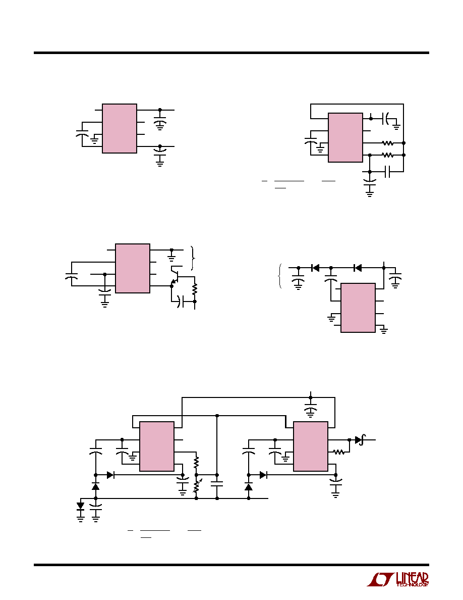
R
X
= V
X
/(4.4 I
OUT
)
where
V
X
V
IN
≠ [(LT1054 Voltage Loss)(1.3) +
|
V
OUT
|
]
and I
OUT
= maximum required output current. The factor of
1.3 will allow some operating margin for the LT1054.
For example: assume a 12V to ≠ 5V converter at 100mA
output current. First calculate the power dissipation with-
out an external resistor:
P = (12V ≠
|
≠ 5V
|
)(100mA) + (12V)(100mA)(0.2)
P = 700mW + 240mW = 940mW
At
JA
of 130
∞
C/W for a commercial plastic device this
would cause a junction temperature rise of 122
∞
C so that
the device would exceed the maximum junction tempera-
ture at an ambient temperature of 25
∞
C. Now calculate the
power dissipation with an external resistor (R
X
). First find
how much voltage can be dropped across R
X
. The maxi-
mum voltage loss of the LT1054 in the standard regulator
configuration at 100mA output current is 1.6V, so
V
X
= 12V ≠ [(1.6V)(1.3) +
|
≠ 5V
|
] = 4.9V and
R
X
= 4.9V/(4.4)(100mA) = 11
This resistor will reduce the power dissipated by the
LT1054 by (4.9V)(100mA) = 490mW. The total power
dissipated by the LT1054 would then be (940mW ≠
490mW) = 450mW. The junction temperature rise would
now be only 58
∞
C. Although commercial devices are
guaranteed to be functional up to a junction temperature
of 125
∞
C, the specifications are only guaranteed up to a
junction temperature of 100
∞
C, so ideally you should limit
the junction temperature to 100
∞
C. For the above example
this would mean limiting the ambient temperature to 42
∞
C.
Other steps can be taken to allow higher ambient tempera-
tures. The thermal resistance numbers for the LT1054
packages represent worst case numbers with no heat
sinking and still air. Small clip-on type heat sinks can be
used to lower the thermal resistance of the LT1054 pack-
age. In some systems there may be some available airflow
which will help to lower the thermal resistance. Wide PC
board traces from the LT1054 leads can also help to
remove heat from the device. This is especially true for
plastic packages.
where dV = peak-to-peak ripple and f = oscillator frequency.
For output capacitors with significant ESR a second term
must be added to account for the voltage step at the switch
transitions. This step is approximately equal to:
(2I
OUT
)(ESR of C
OUT
)
Power Dissipation
The power dissipation of any LT1054 circuit must be
limited such that the junction temperature of the device
does not exceed the maximum junction temperature rat-
ings. The total power dissipation must be calculated from
two components, the power loss due to voltage drops in the
switches and the power loss due to drive current losses.
The total power dissipated by the LT1054 can be calculated
from:
P
(V
IN
≠
|
V
OUT
|
)(I
OUT
) + (V
IN
)(I
OUT
)(0.2)
where both V
IN
and V
OUT
are referred to the ground pin (Pin
3) of the LT1054. For LT1054 regulator circuits, the power
dissipation will be equivalent to that of a linear regulator.
Due to the limited power handling capability of the LT1054
packages, the user will have to limit output current require-
ments or take steps to dissipate some power external to the
LT1054 for large input/output differentials. This can be
accomplished by placing a resistor in series with C
IN
as
shown in Figure 6. A portion of the input voltage will then
be dropped across this resistor without affecting the output
regulation. Because switch current is approximately 2.2
times the output current and the resistor will cause a
voltage drop when C
IN
is both charging and discharging,
the resistor should be chosen as:
C1
R2
C
IN
C
OUT
V
OUT
LT1054 ∑ F06
V
IN
R1
RX
LT1054
FB/SHDN
CAP
+
GND
CAP
≠
V
+
OSC
V
REF
V
OUT
+
+
Figure 6
10
LT1054/LT1054L
TYPICAL APPLICATIO
N
S
N
U
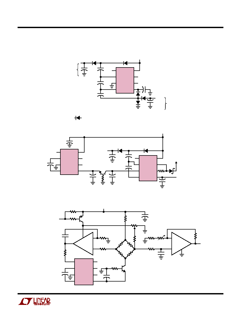
Basic Voltage Inverter
Positive Doubler
Negative Voltage Doubler
100mA Regulating Negative Doubler
1N4002
HP5082-2810
V
IN
3.5 TO 15V
20k
1N4002
0.002
µ
F
LT1054 ∑ TAO6
2.2
µ
F
R1
40k
V
OUT
SET
PIN 2
LT1054 #1
≠V
OUT
I
OUT
100mA MAX
R2
500k
1N4002
1N4002
1N4002
, REFER TO FIGURE 5
V
IN
= 3.5 TO 15V
V
OUT
MAX
≠2V
IN
+ [1054 VOLTAGE LOSS + 2(V
DIODE
)]
R2
R1
=
=
+ 1
|
V
OUT
|
)
)
V
REF
2
≠ 40mV
)
)
+ 1
|
V
OUT
|
1.21V
10
µ
F
10
µ
F
100
µ
F
+
+
+
10
µ
F
+
10
µ
F
10
µ
F
+
+
+
10
µ
F
+
LT1054 #1
FB/SHDN
CAP
+
GND
CAP
≠
V
+
OSC
V
REF
V
OUT
LT1054 #2
FB/SHDN
CAP
+
GND
CAP
≠
V
+
OSC
V
REF
V
OUT
Basic Voltage Inverter/Regulator
0.002
µ
F
R2
10
µ
F
100
µ
F
REFER TO FIGURE 5
2
µ
F
V
OUT
LT1054 ∑ TA03
V
IN
R1
R2
R1
=
=
+ 1
|
V
OUT
|
)
)
V
REF
2
≠ 40mV
)
)
+ 1 ,
|
V
OUT
|
1.21V
LT1054
FB/SHDN
CAP
+
GND
CAP
≠
V
+
OSC
V
REF
V
OUT
+
+
+
100
µ
F
V
IN
≠V
OUT
LT1054 ∑ TAO2
LT1054
FB/SHDN
CAP
+
GND
CAP
≠
V
+
OSC
V
REF
V
OUT
2
µ
F
100
µ
F
+
+
+
2
µ
F
100
µ
F
V
IN
= ≠3.5V TO ≠15V
V
OUT
= 2V
IN
+ (LT1054 VOLTAGE LOSS) + (Q
X
SATURATION VOLTAGE)
*SEE FIGURE 3
V
IN
V
IN
V
OUT
LT1054 ∑ TAO4
R
X
*
+
≠
100
µ
F
+
+
+
LT1054
FB/SHDN
CAP
+
GND
CAP
≠
V
+
OSC
V
REF
V
OUT
Q
X
*
1N4001
V
IN
= 3.5V TO 15V
V
OUT
2V
IN
≠ (V
L
+ 2V
DIODE
)
V
L
= LT1054 VOLTAGE LOSS
V
IN
3.5V TO 15V
LT1054 ∑ TAO5
1N4001
V
OUT
50mA
+
≠
100
µ
F
2
µ
F
10
µ
F
+
+
+
LT1054
FB/SHDN
CAP
+
GND
CAP
≠
V
+
OSC
V
REF
V
OUT
11
LT1054/LT1054L
TYPICAL APPLICATIO
N
S
N
U
5V to
±
12V Converter
Bipolar Supply Doubler
20k
1N914
1N914
V
IN
= 5V
TO PIN 4
LT1054 #1
V
OUT
≠12V
I
OUT
= 25mA
V
OUT
12V
I
OUT
= 25mA
LT1054 ∑ TAO8
1k
2N2219
10
µ
F
100
µ
F
10
µ
F
10
µ
F
100
µ
F
5
µ
F
100
µ
F
5
µ
F
+
+
+
+
+
+
+
+
LT1054 #2
FB/SHDN
CAP
+
GND
CAP
≠
V
+
OSC
V
REF
V
OUT
LT1054 #1
FB/SHDN
CAP
+
GND
CAP
≠
V
+
OSC
V
REF
V
OUT
V
IN
3.5V TO 15V
≠V
OUT
LT1054 ∑ TAO7
+V
OUT
+
≠
+
≠
= 1N4001
V
IN
= 3.5V TO 15V
+V
OUT
2V
IN
≠ (V
L
+ 2V
DIODE
)
≠V
OUT
≠2V
IN
+ (V
L
+ 2V
DIODE
)
V
L
= LT1054 VOLTAGE LOSS
100
µ
F
10
µ
F
10
µ
F
10
µ
F
100
µ
F
100
µ
F
+
+
+
+
+
+
LT1054
FB/SHDN
CAP
+
GND
CAP
≠
V
+
OSC
V
REF
V
OUT
1
µ
F
5V
1
2
3
8
200k
3k
100
µ
F
TANTALUM
LT1054 ∑ TAO9
0.022
µ
F
≠
+
2N2222
A = 125 FOR 0V TO 3V OUT FROM FULL-SCALE
BRIDGE OUTPUT OF 24mV
100k
100k
10k
ZERO
TRIM
5k
GAIN
TRIM
10k
10k
5V
40
301k
1M
A1
1/2 LT1013
5k
6
5
4
7
10k
2N2907
INPUT TTL
OR CMOS
LOW FOR ON
350
≠
+
A2
1/2 LT1013
10
µ
F
+
+
10
µ
F
+
LT1054
FB/SHDN
CAP
+
GND
CAP
≠
V
+
OSC
V
REF
V
OUT
Strain Gauge Bridge Signal Conditioner
12
LT1054/LT1054L
TYPICAL APPLICATIO
N
S
N
U
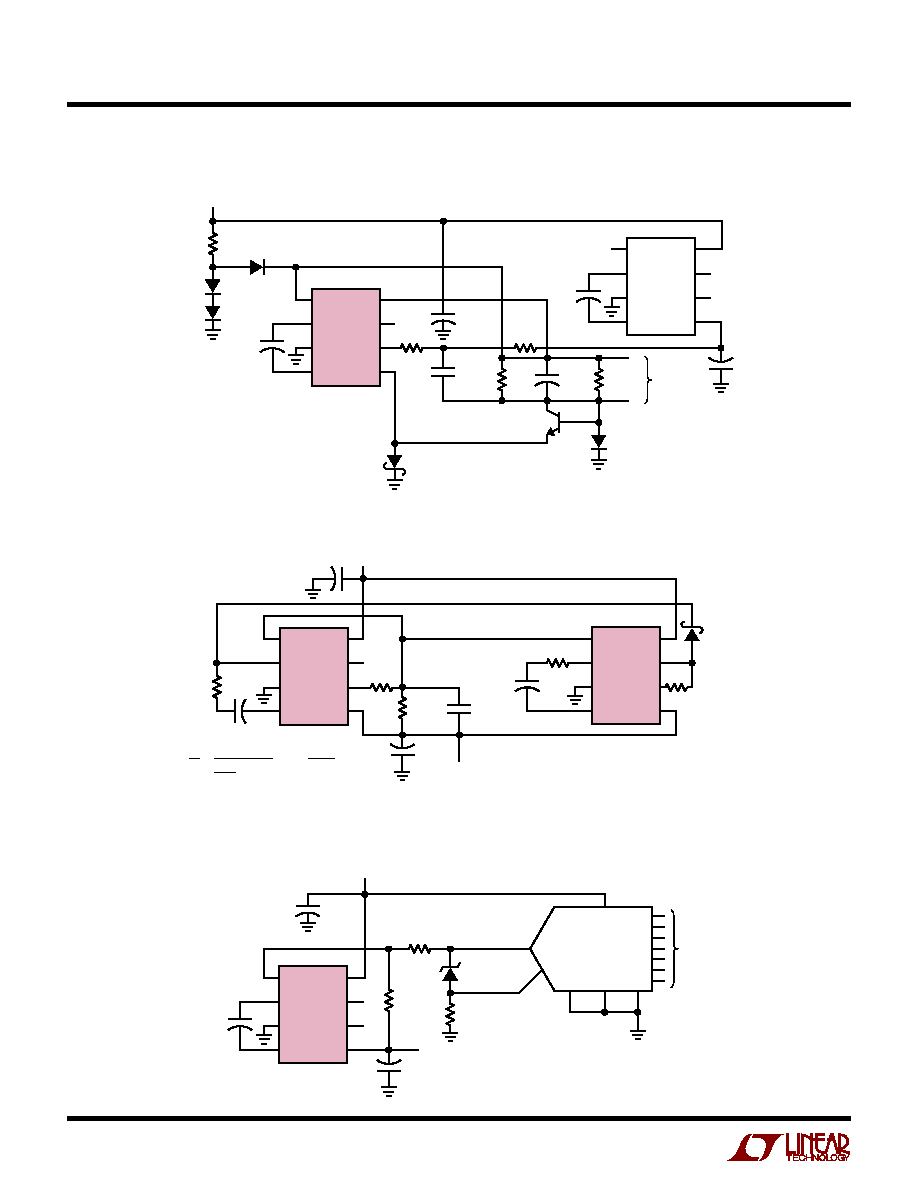
3.5V to 5V Regulator
Regulating 200mA, 12V to ≠ 5V Converter
Digitally Programmable Negative Supply
20k
V
OUT
= ≠V
IN
(PROGRAMMED)
20k
15V
LT1004-2.5
2.5V
LT1054 ∑ TA12
AD558
16
11
14
DIGITAL
INPUT
13
12
10
µ
F
5
µ
F
+
100
µ
F
+
+
LT1054
FB/SHDN
CAP
+
GND
CAP
≠
V
+
OSC
V
REF
V
OUT
0.002
µ
F
HP5082-2810
V
OUT
= ≠5V
I
OUT
= 0mA to 200mA
12V
R1
39.2k
R2
200k
20k
10
1/2W
LT1054 ∑ TA11
10
1/2W
10
µ
F
5
µ
F
200
µ
F
10
µ
F
+
+
+
+
LT1054 #1
FB/SHDN
CAP
+
GND
CAP
≠
V
+
OSC
V
REF
V
OUT
LT1054 #2
FB/SHDN
CAP
+
GND
CAP
≠
V
+
OSC
V
REF
V
OUT
REFER TO FIGURE 5
R2
R1
=
=
+ 1
|
V
OUT
|
)
)
V
REF
2
≠ 40mV
)
)
+ 1 ,
|
V
OUT
|
1.21V
5
µ
F
100
µ
F
20k
1N914
R1
20k
1N914
V
IN
= 3.5V TO 5.5V
V
OUT
= 5V
I
OUT(MAX)
= 50mA
1N914
1N5817
V
IN
3.5V TO 5.5V
LT1054 ∑ TA10
LTC1044
1
2
3
4
8
7
6
5
1
µ
F
1
µ
F
0.002
µ
F
R2
125k
3k
1N914
R2
125k
2N2219
V
OUT
= 5V
+
≠
10
µ
F
+
+
+
+
+
LT1054
FB/SHDN
CAP
+
GND
CAP
≠
V
+
OSC
V
REF
V
OUT
13
LT1054/LT1054L
Dimensions in inches (millimeters) unless otherwise noted.
PACKAGE DESCRIPTIO
N
U
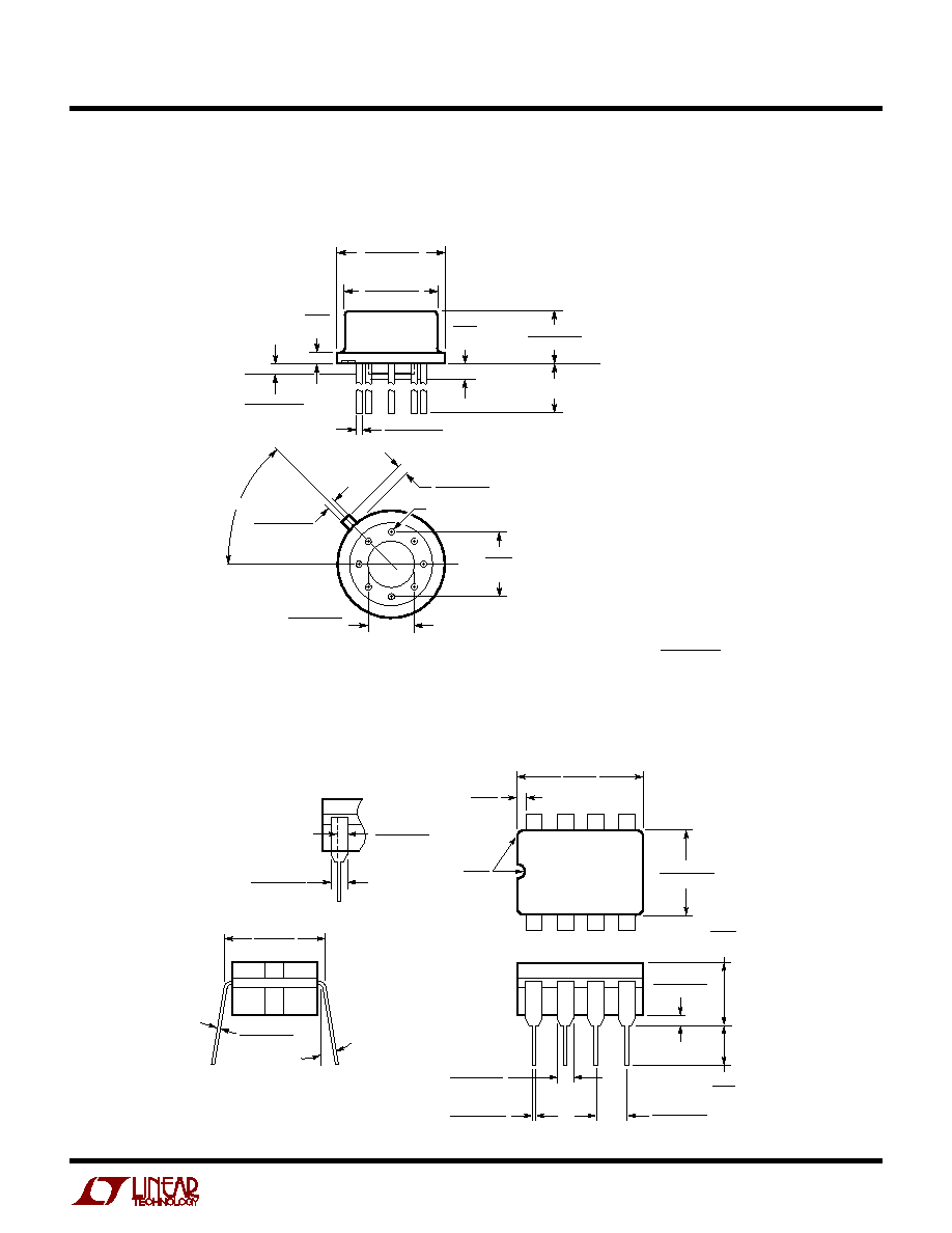
H Package
8-Lead TO-5 Metal Can (0.200 PCD)
(LTC DWG # 05-08-1320)
J8 1197
0.014 ≠ 0.026
(0.360 ≠ 0.660)
0.200
(5.080)
MAX
0.015 ≠ 0.060
(0.381 ≠ 1.524)
0.125
3.175
MIN
0.100
±
0.010
(2.540
±
0.254)
0.300 BSC
(0.762 BSC)
0.008 ≠ 0.018
(0.203 ≠ 0.457)
0
∞
≠ 15
∞
0.005
(0.127)
MIN
0.405
(10.287)
MAX
0.220 ≠ 0.310
(5.588 ≠ 7.874)
1
2
3
4
8
7
6
5
0.025
(0.635)
RAD TYP
0.045 ≠ 0.068
(1.143 ≠ 1.727)
FULL LEAD
OPTION
0.023 ≠ 0.045
(0.584 ≠ 1.143)
HALF LEAD
OPTION
CORNER LEADS OPTION
(4 PLCS)
0.045 ≠ 0.068
(1.143 ≠ 1.727)
NOTE: LEAD DIMENSIONS APPLY TO SOLDER DIP/PLATE
OR TIN PLATE LEADS
J8 Package
8-Lead CERDIP (Narrow 0.300, Hermetic)
(LTC DWG # 05-08-1110)
0.050
(1.270)
MAX
0.016 ≠ 0.021**
(0.406 ≠ 0.533)
0.010 ≠ 0.045*
(0.254 ≠ 1.143)
SEATING
PLANE
0.040
(1.016)
MAX
0.165 ≠ 0.185
(4.191 ≠ 4.699)
GAUGE
PLANE
REFERENCE
PLANE
0.500 ≠ 0.750
(12.700 ≠ 19.050)
0.305 ≠ 0.335
(7.747 ≠ 8.509)
0.335 ≠ 0.370
(8.509 ≠ 9.398)
DIA
0.200
(5.080)
TYP
0.027 ≠ 0.045
(0.686 ≠ 1.143)
0.028 ≠ 0.034
(0.711 ≠ 0.864)
0.110 ≠ 0.160
(2.794 ≠ 4.064)
INSULATING
STANDOFF
45
∞
TYP
H8(TO-5) 0.200 PCD 1197
LEAD DIAMETER IS UNCONTROLLED BETWEEN THE REFERENCE PLANE
AND 0.045" BELOW THE REFERENCE PLANE
FOR SOLDER DIP LEAD FINISH, LEAD DIAMETER IS
0.016 ≠ 0.024
(0.406 ≠ 0.610)
*
**
PIN 1
14
LT1054/LT1054L
Dimensions in inches (millimeters) unless otherwise noted.
PACKAGE DESCRIPTIO
N
U
N8 1197
0.100
±
0.010
(2.540
±
0.254)
0.065
(1.651)
TYP
0.045 ≠ 0.065
(1.143 ≠ 1.651)
0.130
±
0.005
(3.302
±
0.127)
0.020
(0.508)
MIN
0.018
±
0.003
(0.457
±
0.076)
0.125
(3.175)
MIN
1
2
3
4
8
7
6
5
0.255
±
0.015*
(6.477
±
0.381)
0.400*
(10.160)
MAX
0.009 ≠ 0.015
(0.229 ≠ 0.381)
0.300 ≠ 0.325
(7.620 ≠ 8.255)
0.325
+0.035
≠0.015
+0.889
≠0.381
8.255
(
)
*THESE DIMENSIONS DO NOT INCLUDE MOLD FLASH OR PROTRUSIONS.
MOLD FLASH OR PROTRUSIONS SHALL NOT EXCEED 0.010 INCH (0.254mm)
N8 Package
8-Lead PDIP (Narrow 0.300)
(LTC DWG # 05-08-1510)
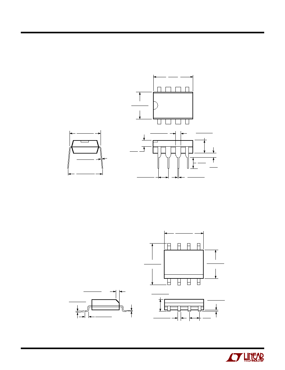
S8 Package
8-Lead Plastic Small Outline (Narrow 0.150)
(LTC DWG # 05-08-1610)
SO8 0996
0.053 ≠ 0.069
(1.346 ≠ 1.752)
0.014 ≠ 0.019
(0.355 ≠ 0.483)
0.004 ≠ 0.010
(0.101 ≠ 0.254)
0.050
(1.270)
TYP
0.016 ≠ 0.050
0.406 ≠ 1.270
0.010 ≠ 0.020
(0.254 ≠ 0.508)
◊
45
∞
0
∞
≠ 8
∞
TYP
0.008 ≠ 0.010
(0.203 ≠ 0.254)
1
2
3
4
0.150 ≠ 0.157**
(3.810 ≠ 3.988)
8
7
6
5
0.189 ≠ 0.197*
(4.801 ≠ 5.004)
0.228 ≠ 0.244
(5.791 ≠ 6.197)
DIMENSION DOES NOT INCLUDE MOLD FLASH. MOLD FLASH
SHALL NOT EXCEED 0.006" (0.152mm) PER SIDE
DIMENSION DOES NOT INCLUDE INTERLEAD FLASH. INTERLEAD
FLASH SHALL NOT EXCEED 0.010" (0.254mm) PER SIDE
*
**
15
LT1054/LT1054L
Dimensions in inches (millimeters) unless otherwise noted.
PACKAGE DESCRIPTIO
N
U
Information furnished by Linear Technology Corporation is believed to be accurate and reliable.
However, no responsibility is assumed for its use. Linear Technology Corporation makes no represen-
tation that the interconnection of its circuits as described herein will not infringe on existing patent rights.
S16 (WIDE) 0396
NOTE 1
0.398 ≠ 0.413*
(10.109 ≠ 10.490)
16
15
14
13
12
11
10
9
1
2
3
4
5
6
7
8
0.394 ≠ 0.419
(10.007 ≠ 10.643)
0.037 ≠ 0.045
(0.940 ≠ 1.143)
0.004 ≠ 0.012
(0.102 ≠ 0.305)
0.093 ≠ 0.104
(2.362 ≠ 2.642)
0.050
(1.270)
TYP
0.014 ≠ 0.019
(0.356 ≠ 0.482)
TYP
0
∞
≠ 8
∞
TYP
NOTE 1
0.009 ≠ 0.013
(0.229 ≠ 0.330)
0.016 ≠ 0.050
(0.406 ≠ 1.270)
0.291 ≠ 0.299**
(7.391 ≠ 7.595)
◊
45
∞
0.010 ≠ 0.029
(0.254 ≠ 0.737)
NOTE:
1. PIN 1 IDENT, NOTCH ON TOP AND CAVITIES ON THE BOTTOM OF PACKAGES ARE THE MANUFACTURING OPTIONS.
THE PART MAY BE SUPPLIED WITH OR WITHOUT ANY OF THE OPTIONS
DIMENSION DOES NOT INCLUDE MOLD FLASH. MOLD FLASH SHALL NOT EXCEED 0.006" (0.152mm) PER SIDE
DIMENSION DOES NOT INCLUDE INTERLEAD FLASH. INTERLEAD FLASH SHALL NOT EXCEED 0.010" (0.254mm) PER SIDE
*
**
SW Package
16-Lead Plastic Small Outline (Wide 0.300)
(LTC DWG # 05-08-1620)
16
LT1054/LT1054L
©
LINEAR TECHNOLOGY CORPORATION 1987
1054ld LT/TP 1298 2K REV D ∑ PRINTED IN USA
TYPICAL APPLICATIO
N
S
N
U
Negative Doubler with Regulator
2
µ
F
V
IN
3.5V TO 15V
100
µ
F
R2
1M
1N4001
1N4001
LT1054 ∑ TA14
100
µ
F
0.002
µ
F
≠V
OUT
V
IN
= 3.5V TO 15V
V
OUT(MAX)
≠2V
IN
+ (V
L
+ 2V
DIODE
)
V
L
= LT1054 VOLTAGE LOSS
, REFER TO FIGURE 5
R2
R1
=
=
+ 1
|
V
OUT
|
)
)
V
REF
2
≠ 40mV
)
)
+ 1
|
V
OUT
|
1.21V
10
µ
F
+
+
+
+
10
µ
F
+
LT1054
FB/SHDN
CAP
+
GND
CAP
≠
V
+
OSC
V
REF
V
OUT
R1, 20k
0.03
µ
F
V
IN
= 5V
50k
1N5817
1N5817
LT1054 ∑ TA13
≠
+
10k
10k
10k
5.5k
2.5k
0.1
µ
F
5V
LT1006
100
µ
F
V
OUT
8V
50mA
2
µ
F
10
µ
F
+
+
+
LT1054
FB/SHDN
CAP
+
GND
CAP
≠
V
+
OSC
V
REF
V
OUT
Positive Doubler with Regulation
Linear Technology Corporation
1630 McCarthy Blvd., Milpitas, CA 95035-7417
(408) 432-1900
q
FAX: (408) 434-0507
q
www.linear-tech.com
RELATED PARTS
PART NUMBER
DESCRIPTION
COMMENTS
LTC1144
Switched-Capacitor Voltage Converter
Wide Input Voltage Range, 2V to 18V
LTC1514/LTC1515
Step-Up/Step-Down Switched Capacitor DC/DC Converters
Regulated 5V Doublers
LT1611
Micropower Inverting DC/DC Converter
150mA Output
LT1614
Micropower Inverting DC/DC Converter
250mA Output
THE TYPICAL APPLICATIONS CIRCUITS WERE VERIFIED USING THE STANDARD LT1054. FOR S8 APPLICATIONS
ASSISTANCE IN ANY OF THE UNUSUAL APPLICATIONS CIRCUITS PLEASE CONSULT THE FACTORY