 | –≠–ª–µ–∫—Ç—Ä–æ–Ω–Ω—ã–π –∫–æ–º–ø–æ–Ω–µ–Ω—Ç: LT1055N8 | –°–∫–∞—á–∞—Ç—å:  PDF PDF  ZIP ZIP |
1
LT1055/LT1056
10556fb
Precision, High Speed,
JFET Input Operational Amplifiers
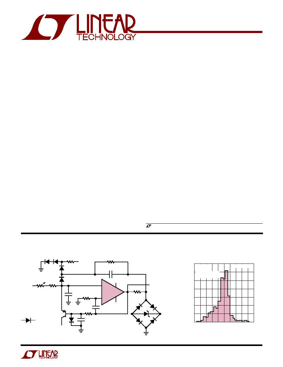
≠
+
0V TO 10V
INPUT
10kHZ
TRIM
5k
4.7k
15V
2N3906
15V
≠15V
LT1055/56 TA01
≠15V
= 1N4148
3M
0.001 (POLYSTYRENE)
0.1
µ
F
THE LOW OFFSET VOLTAGE OF LT1056
CONTRIBUTES ONLY 0.1Hz OF ERROR
WHILE ITS HIGH SLEW RATE PERMITS
10kHz OPERATION.
0.1
µ
F
22k
1.5k
LM329
3.3M
7
6
4
3
2
33pF
*1% FILM
OUTPUT
1Hz TO 10kHz
0.005%
LINEARITY
LT1056
s
Guaranteed Offset Voltage: 150
µ
V Max
≠55
∞
C to 125
∞
C: 500
µ
V Max
s
Guaranteed Drift: 4
µ
V/
∞
C Max
s
Guaranteed Bias Current
70
∞
C: 150pA Max
125
∞
C: 2.5nA Max
s
Guaranteed Slew Rate: 12V/
µ
s Min
s
Precision, High Speed Instrumentation
s
Logarithmic Amplifiers
s
D/A Output Amplifiers
s
Photodiode Amplifiers
s
Voltage-to-Frequency Converters
s
Frequency-to-Voltage Converters
s
Fast, Precision Sample-and-Hold
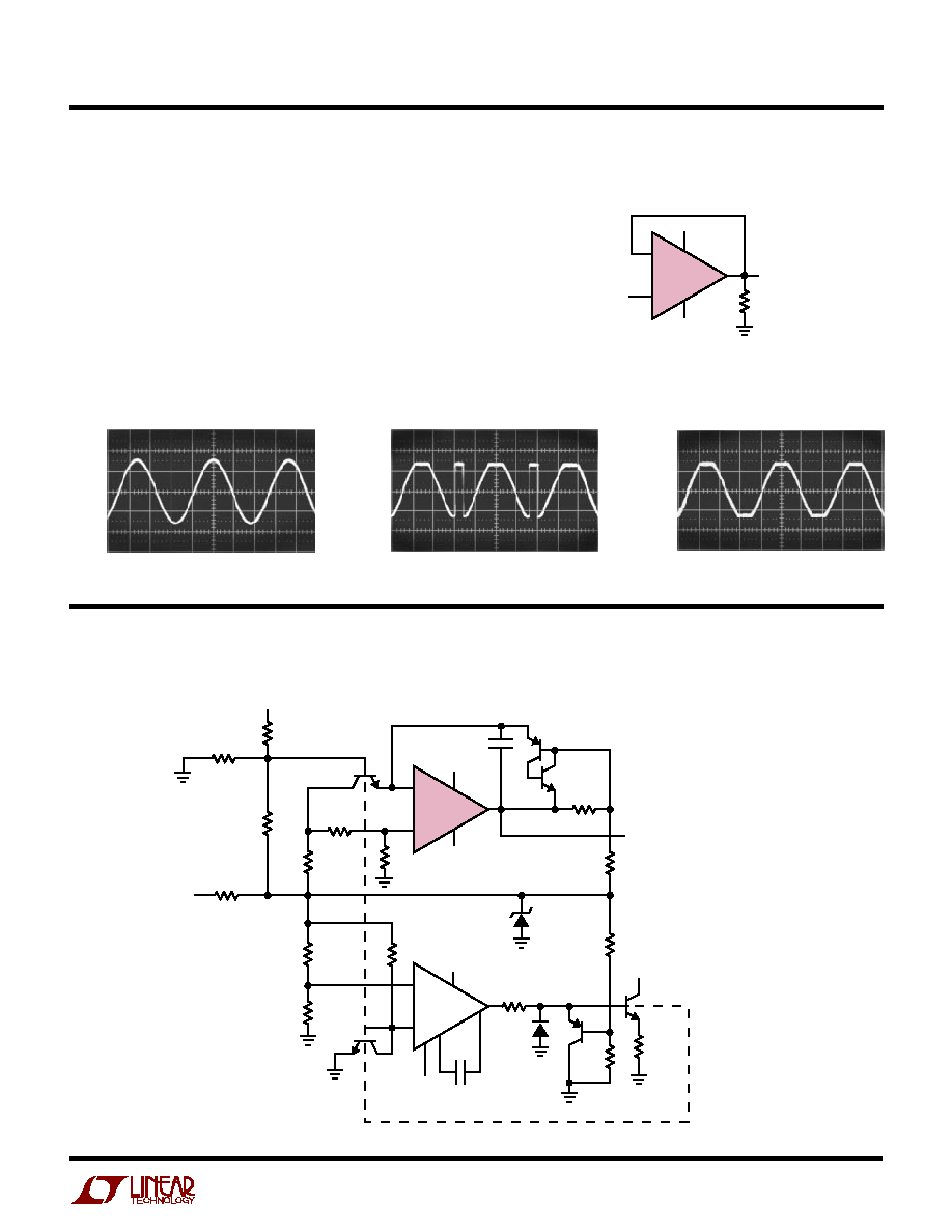
The LT
Æ
1055/LT1056 JFET input operational amplifiers
combine precision specifications with high speed perfor-
mance.
For the first time, 16V/
µ
s slew rate and 6.5MHz gain
bandwidth product are simultaneously achieved with off-
set voltage of typically 50
µ
V, 1.2
µ
V/
∞
C drift, bias currents
of 40pA at 70
∞
C and 500pA at 125
∞
C.
The 150
µ
V maximum offset voltage specification is the
best available on any JFET input operational amplifier.
The LT1055 and LT1056 are differentiated by their operat-
ing currents. The lower power dissipation LT1055 achieves
lower bias and offset currents and offset voltage. The
additional power dissipation of the LT1056 permits higher
slew rate, bandwidth and faster settling time with a slight
sacrifice in DC performance.
The voltage-to-frequency converter shown below is one of
the many applications which utilize both the precision and
high speed of the LT1055/LT1056.
For a JFET input op amp with 23V/
µ
s guaranteed slew rate,
refer to the LT1022 data sheet.
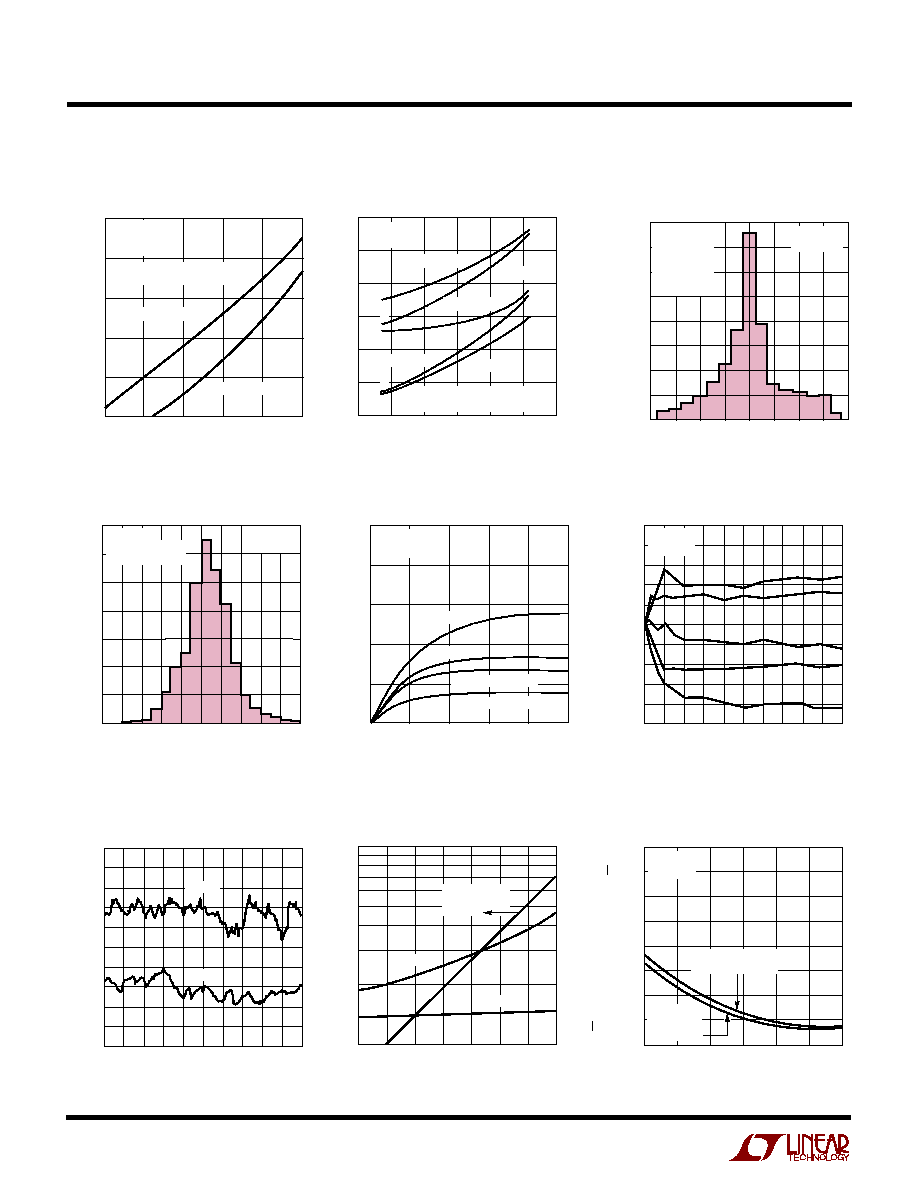
Distribution of Input Offset Voltage
(H Package)
0kHz to 10kHz Voltage-to-Frequency Converter
INPUT OFFSET VOLTAGE (
µ
V)
0
NUMBER OF UNITS
20
60
80
100
140
≠400
0
200
LT1055/56 TA02
40
120
400
≠200
V
S
=
±
15V
T
A
= 25
∞
C
634 UNITS TESTED
FROM THREE RUNS
50% TO
±
60
µ
V
APPLICATIO S
U
FEATURES
TYPICAL APPLICATIO
U
DESCRIPTIO
U
, LTC and LT are registered trademarks of Linear Technology Corporation.
2
LT1055/LT1056
10556fb
Supply Voltage ......................................................
±
20V
Differential Input Voltage .......................................
±
40V
Input Voltage .........................................................
±
20V
Output Short-Circuit Duration .......................... Indefinite
Operating Temperature Range
LT1055AM/LT1055M/LT1056AM/
LT1056M (OBSOLETE) .............. ≠55
∞
C to 125
∞
C
ABSOLUTE
M
AXI
M
U
M
RATINGS
W
W
W
U
PACKAGE/ORDER I
N
FOR
M
ATIO
N
W
U
U
ORDER PART
NUMBER
LT1055S8
LT1056S8
Consult LTC Marketing for parts specified with wider operating temperature ranges.
1
2
3
4
8
7
6
5
TOP VIEW
BAL
≠IN
+
IN
V
≠
N/C
V
+
OUT
BAL
N8 PACKAGE
8-LEAD PDIP
T
JMAX
= 150
∞
C,
JA
= 130
∞
C/ W
LT1055ACH
LT1055CH
LT1055AMH
LT1055MH
TOP VIEW
NC
BALANCE
OUT
BALANCE
+
IN
V
≠
8
7
6
5
3
2
1
4
H PACKAGE
8-LEAD TO-5 METAL CAN
≠IN
V
+
T
JMAX
= 150
∞
C,
JA
= 150
∞
C/ W,
JC
= 45
∞
C/ W
ORDER PART
NUMBER
OBSOLETE PACKAGE
Consider the N8 Package for Alternate Source
(Note 1)
1
2
3
4
8
7
6
5
TOP VIEW
S8 PACKAGE
8-LEAD PLASTIC SO
BAL
≠IN
+
IN
V
≠
N/C
V
+
OUT
BAL
LT1055CN8
LT1056CN8
ORDER PART
NUMBER
T
JMAX
= 150
∞
C,
JA
= 150
∞
C/ W
LT1056ACH
LT1056CH
LT1056AMH
LT1056MH
T
A
= 25
∞
C. V
S
=
±
15V, V
CM
= 0V unless otherwise noted.
ELECTRICAL CHARACTERISTICS
LT1055M/LT1056M
LT1055AM/LT1056AM
LT1055CH/LT1056CH
LT1055AC/LT1056AC
LT1055CN8/LT1056CN8
SYMBOL
PARAMETER
CONDITIONS
MIN
TYP
MAX
MIN
TYP
MAX
UNITS
V
OS
Input Offset Voltage (Note 2)
LT1055 H Package
--
50
150
--
70
400
µ
V
LT1056 H Package
--
50
180
--
70
450
µ
V
LT1055 N8 Package
--
--
--
--
120
700
µ
V
LT1056 N8 Package
--
--
--
--
140
800
µ
V
I
OS
Input Offset Current
Fully Warmed Up
--
2
10
--
2
20
pA
I
B
Input Bias Current
Fully Warmed Up
--
±
10
±
50
--
±
10
±
50
pA
V
CM
= 10V
--
30
130
--
30
150
pA
LT1055AC/LT1055C/LT1056AC/
LT1056C ................................................ 0
∞
C to 70
∞
C
Storage Temperature Range
All Devices ...................................... ≠ 65
∞
C to 150
∞
C
Lead Temperature (Soldering, 10 sec).................. 300
∞
C
1055
1056
S8 PART
MARKING
3
LT1055/LT1056
10556fb
LT1055M/LT1056M
LT1055AM/LT1056AM
LT1055CH/LT1056CH
LT1055AC/LT1056AC
LT1055CN8/LT1056CN8
SYMBOL
PARAMETER
CONDITIONS
MIN
TYP
MAX
MIN
TYP
MAX
UNITS
Input Resistance:Differential
--
10
12
--
--
10
12
--
Common Mode V
CM
= ≠11V to 8V
--
10
12
--
--
10
12
--
V
CM
= 8V to 11V
--
10
11
--
--
10
11
--
Input Capacitance
--
4
--
--
4
--
pF
e
n
Input Noise Voltage
0.1Hz to 10Hz
LT1055
--
1.8
--
--
2.0
--
µ
V
P-P
LT1056
--
2.5
--
--
2.8
--
µ
V
P-P
Input Noise Voltage Density
f
0
= 10Hz (Note 3)
--
28
50
--
30
60
nV/
Hz
f
0
= 1kHz (Note 4)
--
14
20
--
15
22
nV/
Hz
I
n
Input Noise Current Density
f
0
= 10Hz, 1kHz (Note 5)
--
1.8
4
--
1.8
4
fA/
Hz
A
VOL
Large-Signal Voltage Gain
V
0
=
±
10V
R
L
= 2k
150
400
--
120
400
--
V/mV
R
L
= 1k
130
300
--
100
300
--
V/mV
Input Voltage Range
±
11
±
12
--
±
11
±
12
--
V
CMRR
Common Mode Rejection Ratio
V
CM
=
±
11V
86
100
--
83
98
--
dB
PSRR
Power Supply Rejection Ratio
V
S
=
±
10V to
±
18V
90
106
--
88
104
--
dB
V
OUT
Output Voltage Swing
R
L
= 2k
±
12
±
13.2
--
±
12
±
13.2
--
V
SR
Slew Rate
LT1055
10
13
--
7.5
12
--
V/
µ
s
LT1056
12
16
--
9.0
14
--
V/
µ
s
GBW
Gain Bandwidth Product
f = 1MHz
LT1055
--
5.0
--
--
4.5
--
MHz
LT1056
--
6.5
--
--
5.5
--
MHz
I
S
Supply Current
LT1055
--
2.8
4.0
--
2.8
4.0
mA
LT1056
--
5.0
6.5
--
5.0
7.0
mA
Offset Voltage Adjustment Range R
POT
= 100k
--
±
5
--
--
±
5
--
mV
T
A
= 25
∞
C. V
S
=
±
15V, V
CM
= 0V unless otherwise noted.
ELECTRICAL CHARACTERISTICS
LT1055AC
LT1055CH/LT1056CH
LT1056AC
LT1055CN8/LT1056CN8
SYMBOL
PARAMETER
CONDITIONS
MIN
TYP
MAX
MIN
TYP
MAX
UNITS
V
OS
Input Offset Voltage (Note 2)
LT1055 H Package
q
--
100
330
--
140
750
µ
V
LT1056 H Package
q
--
100
360
--
140
800
µ
V
LT1055 N8 Package
q
--
--
--
--
250
1250
µ
V
LT1056 N8 Package
q
--
--
--
--
280
1350
µ
V
Average Temperature
H Package (Note 6)
q
--
1.2
4.0
--
1.6
8.0
µ
V/
∞
C
Coefficient of Input Offset
N8 Package (Note 6)
q
--
--
--
--
3.0
12.0
µ
V/
∞
C
Voltage
I
OS
Input Offset Current
Warmed Up
LT1055
q
--
10
50
--
16
80
pA
T
A
= 70
∞
C
LT1056
q
--
14
70
--
18
100
pA
I
B
Input Bias Current
Warmed Up
LT1055
q
--
±
30
±
150
--
±
40
±
200
pA
T
A
= 70
∞
C
LT1056
q
--
±
40
±
80
--
±
50
±
240
pA
A
VOL
Large-Signal Voltage Gain
V
O
=
±
10V, R
L
= 2k
q
80
250
--
60
250
--
V/mV
CMRR
Common Mode Rejection Ratio
V
CM
=
±
10.5V
q
85
100
--
82
98
--
dB
PSRR
Power Supply Rejection Ratio
V
S
=
±
10V to
±
18V
q
89
105
--
87
103
--
dB
V
OUT
Output Voltage Swing
R
L
= 2k
q
±
12
±
13.1
--
±
12
±
13.1
--
V
The
q
denotes the specifications which apply over the temperature range 0
∞
C
T
A
70
∞
C.
V
S
=
±
15V, V
CM
= 0V unless otherwise noted.
4
LT1055/LT1056
10556fb
LT1055AM
LT1055M
LT1056AM
LT1056M
SYMBOL
PARAMETER
CONDITIONS
MIN
TYP
MAX
MIN
TYP
MAX
UNITS
V
OS
Input Offset Voltage (Note 2)
LT1055
q
--
180
500
--
250
1200
µ
V
LT1056
q
--
180
550
--
250
1250
µ
V
Average Temperature
(Note 6)
q
--
1.3
4.0
--
1.8
8.0
µ
V/
∞
C
Coefficient of Input Offset
Voltage
I
OS
Input Offset Current
Warmed Up
LT1055
q
--
0.20
1.2
--
0.25
1.8
nA
T
A
= 125
∞
C
LT1056
q
--
0.25
1.5
--
0.30
2.4
nA
I
B
Input Bias Current
Warmed Up
LT1055
q
--
±
0.4
±
2.5
--
±
0.5
±
4.0
nA
T
A
= 125
∞
C
LT1056
q
--
±
0.5
±
3.0
--
±
0.6
±
5.0
nA
A
VOL
Large-Signal Voltage Gain
V
O
=
±
10V, R
L
= 2k
q
40
120
--
35
120
--
V/mV
CMRR
Common Mode Rejection Ratio
V
CM
=
±
10.5V
q
85
100
--
82
98
--
dB
PSRR
Power Supply Rejection Ratio
V
S
=
±
10V to
±
17V
q
88
104
--
86
102
--
dB
V
OUT
Output Voltage Swing
R
L
= 2k
q
±
12
±
12.9
--
±
12
±
12.9
--
V
ELECTRICAL CHARACTERISTICS
The
q
denotes the specifications which apply over the temperature range
≠55
∞
C
T
A
125
∞
C. V
S
=
±
15V, V
CM
= 0V, unless otherwise noted.
T
A
= 25
∞
C. V
S
=
±
15V, V
CM
= 0V unless otherwise noted.
LT1055CS8/LT1056CS8
SYMBOL
PARAMETER
CONDITIONS
MIN
TYP
MAX
UNITS
V
OS
Input Offset Voltage (Note 2)
500
1500
µ
V
I
OS
Input Offset Current
Fully Warmed Up
5
30
pA
I
B
Input Bias Current
Fully Warmed Up
±
30
±
100
pA
V
CM
= 10V
30
150
pA
Input Resistance
Differential
0.4
T
Common Mode
V
CM
= ≠11V to 8V
0.4
T
V
CM
= 8V to 11V
0.05
T
Input Capacitance
4
pF
e
n
Input Noise Voltage
0.1Hz to 10Hz
LT1055
2.5
µ
V
P-P
LT1056
3.5
µ
V
P-P
Input Noise Voltage Density
f
O
= 10Hz (Note 4)
35
70
nV/
Hz
f
O
= 1kHz (Note 4)
15
22
nV/
Hz
i
n
Input Noise Current Density
f
O
= 10Hz, 1kHz (Note 5)
2.5
10
fA/
Hz
A
VOL
Large-Signal Voltage Gain
V
O
=
±
10V
R
L
= 2k
120
400
V/mV
R
L
= 1k
100
300
V/mV
Input Voltage Range
±
11
±
12
V
CMRR
Common Mode Rejection Ratio
V
CM
=
±
11V
83
98
dB
PSRR
Power Supply Rejection Ratio
V
S
=
±
10V to
±
18V
88
104
dB
V
OUT
Output Voltage Swing
R
L
= 2K
±
12
±
13.2
V
SR
Slew Rate
LT1055
7.5
12
V/
µ
s
LT1056
9.0
14
V/
µ
s
GBW
Gain Bandwidth Product
f = 1MHz
LT1055
4.5
MHz
LT1056
5.5
MHz
I
S
Supply Current
LT1055
2.8
4.0
mA
LT1056
5.0
7.0
mA
Offset Voltage Adjustment Range
R
POT
= 100k
±
5
mV

5
LT1055/LT1056
10556fb
For MIL-STD components, please refer to LTC883 data sheet for test
listing and parameters.
Note 1: Absolute Maximum Ratings are those values beyond which the life
of a device may be impaired.
Note 2: Offset voltage is measured under two different conditions:
(a) approximately 0.5 seconds after application of power; (b) at T
A
= 25
∞
C
only, with the chip heated to approximately 38
∞
C for the LT1055 and to
45
∞
C for the LT1056, to account for chip temperature rise when the device
is fully warmed up.
Note 3: 10Hz noise voltage density is sample tested on every lot of A
grades. Devices 100% tested at 10Hz are available on request.
Note 4: This parameter is tested on a sample basis only.
Note 5: Current noise is calculated from the formula: i
n
= (2ql
B
)
1/2
, where
q = 1.6 ∑ 10
≠19
coulomb. The noise of source resistors up to 1G
swamps
the contribution of current noise.
Note 6: Offset voltage drift with temperature is practically unchanged
when the offset voltage is trimmed to zero with a 100k potentiometer
between the balance terminals and the wiper tied to V
+
. Devices tested to
tighter drift specifications are available on request.
ELECTRICAL CHARACTERISTICS
The
q
denotes the specifications which apply over the temperature range
0
∞
C
T
A
70
∞
C. V
S
=
±
15V, V
CM
= 0V, unless otherwise noted.
LT1055CS8/LT1056CS8
SYMBOL
PARAMETER
CONDITIONS
MIN
TYP
MAX
UNITS
V
OS
Input Offset Voltage (Note 2)
q
800
2200
µ
V
Average Temperature Coefficient of Input Offset Voltage
q
4
15
µ
V/
∞
C
I
OS
Input Offset Current
Warmed Up, T
A
= 70
∞
C
q
18
150
pA
I
B
Input Bias Current
Warmed Up, T
A
= 70
∞
C
q
±
60
±
400
pA
A
VOL
Large-Signal Voltage Gain
V
O
=
±
10V, R
L
= 2k
q
60
250
V/mV
CMRR
Common Mode Rejection Ratio
V
CM
=
±
10.5V
q
82
98
dB
PSRR
Power Supply Rejection Ratio
V
S
=
±
10V to
±
18V
q
87
103
dB
V
OUT
Output Voltage Swing
R
L
= 2K
q
±
12
±
13.1
V
6
LT1055/LT1056
10556fb
TYPICAL PERFOR
M
A
N
CE CHARACTERISTICS
U
W
0.1Hz to 10Hz Noise
Warm-Up Drift
Distribution of Offset Voltage Drift
with Temperature (H Package)*
Long Term Drift of
Representative Units
TIME (SECONDS)
0
NOISE VOLTAGE (1
µ
V/DIVISION)
8
LT1055/56 GO7
2
4
6
10
LT1056
LT1055
RMS NOISE VOLTAGE DENSITY (nV/
Hz)
FREQUENCY (Hz)
1
100
30
300
LT1055/56 G09
30
10
3
10
100
300
1000
1000
LT1056
1/f CORNER = 28HZ
LT1055
1/f CORNER
= 20HZ
V
S
=
±
15V
T
A
= 25
∞
C
Voltage Noise vs Frequency
Noise vs Chip Temperature
CHIP TEMPERATURE (
∞
C)
20
1
2
3
5
7
10
10
20
30
50
70
100
40
LT1055/56 G08
0.1Hz TO 10Hz PEAK-TO-PEAK NOISE (
µ
V/
P-P
)
10
80
30
50
60
70
f
0
= 10kHz
f
0
= 1kHz
PEAK-TO-PEAK
NOISE
RMS NOISE VOLTAGE DENSITY (nV/
Hz)
OFFSET VOLTAGE DRIFT WITH TEMPERATURE (
µ
V/
∞
C)
≠10
0
BATTERY VOLTAGE (V)
20
60
80
100
140
≠8
0
4
LT1055/56 G04
40
120
≠2
8
10
≠6 ≠4
2
6
*DISTRIBUTION IN THE PLASTIC (N8) PACKAGE
IS SIGNIFICANTLY WIDER.
V
S
=
±
15V
634 UNITS TESTED
FROM THREE RUNS
50% TO
±
1.5
µ
V/
∞
C
TIME AFTER POWER ON (MINUTES)
0
CHANGE IN OFFSET VOLTAGE (
µ
V)
60
80
100
4
LT1055/56 G05
40
20
0
1
2
3
5
V
S
=
±
15V
T
A
= 25
∞
C
LT1056CN8
LT1055CN8
LT1056 H PACKAGE
LT1055 H PACKAGE
TIME (MONTHS)
0
OFFSET VOLTAGE CHANGE
µ
V)
50
≠50
40
≠40
30
≠30
20
≠20
10
≠10
0
4
LT1055/56 GO6
1
2
3
5
V
S
=
±
15V
T
A
= 25
∞
C
LT1055/56 G02
COMMON MODE INPUT VOLTAGE (V)
≠15
≠120
INPUT BIAS CURRENT, T
A
= 25
∞
C, T
A
= 70
∞
C (pA)
≠80
≠ 40
0
40
120
≠10
≠5
0
5
10
15
80
≠1200
≠800
≠ 400
0
400
1200
800
V
S
=
±
15V
WARMED UP
T
A
= 125
∞
C
T
A
= 125
∞
C
T
A
= 25
∞
C
T
A
= 70
∞
C
T
A
= 70
∞
C
A = POSITIVE INPUT CURRENT
B = NEGATIVE INPUT CURRENT
A
B
B
A
INPUT BIAS CURRENT, T
A
= 125
∞
C (pA)
Input Bias and Offset Currents
vs Temperature
AMBIENT TEMPERATURE (
∞
C)
0
INPUT BIAS AND OFFSET CURRENT (pA)
100
300
1000
100
LT1055/56 G01
30
10
3
25
50
75
125
BIAS OR OFFSET CURRENTS
MAY BE POSITIVE OR NEGATIVE
BIAS CURRENT
OFFSET CURRENT
V
S
=
±
15V
V
CM
= 0V
WARMED UP
Input Bias Current Over the
Common Mode Range
Distribution of Input Offset
Voltage (N8 Package)
INPUT OFFSET VOLTAGE (
µ
V)
≠800
NUMBER OF INPUTS
80
100
120
800
LT1055/56 G03
60
40
0
≠400
0
400
20
160
140
≠600
≠200
200
600
V
S
=
±
15V
T
A
= 25
∞
C
550 UNITS
TESTED FROM
TWO RUNS
(LT1056)
50% YIELD
TO
±
140
µ
V

7
LT1055/LT1056
10556fb
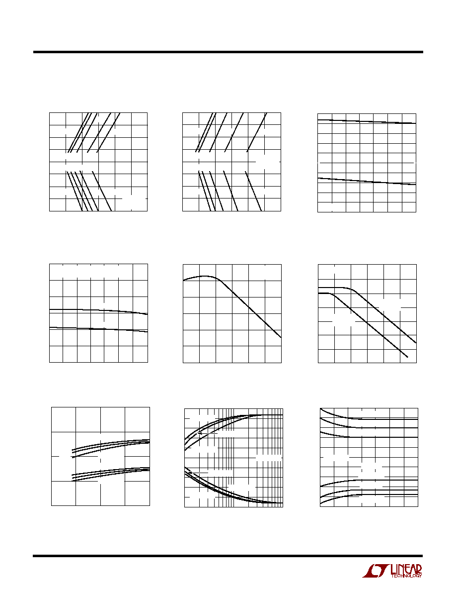
A
V
= 1, C
L
= 100pF, 0.5
µ
s/DIV
5V/DIV
LT1056 Large-Signal Response
TYPICAL PERFOR
M
A
N
CE CHARACTERISTICS
U
W
LT1055/56 G10
LT1055/56 G12
A
V
= 1, C
L
= 100pF, 0.5
µ
s/DIV
5V/DIV
Undistorted Output Swing vs
Frequency
Output Impedence vs Frequency
FREQUENCY (kHz)
1
0.1
OUTPUT IMPEDANCE (
)
1
10
100
10
100
1000
LT1055/56 G15
V
S
=
±
15V
T
A
= 25
∞
C
A
V
= 100
LT1055
LT1056
LT1055
LT1056
LT1056
A
V
= 10
LT1055
A
V
= 1
Gain vs Frequency
FREQUENCY (Hz)
1
GAIN (dB)
60
80
100
100M
LT1055/56 G16
40
20
≠20
100
10k
1M
0
140
120
10
1k
100k
10M
V
S
=
±
15V
T
A
= 25
∞
C
LT1055
LT1056
TEMPERATURE (
∞
C)
≠25
10
100
30
1000
300
25
75
LT1055/56 G18
VOLTAGE GAIN (V/mV)
≠75
125
R
L
= 1k
R
L
= 2k
V
S
=
±
15V
V
O
=
±
10V
Voltage Gain vs Temperature
FREQUENCY (MHz)
0.1
0
PEAK-TO-PEAK OUTPUT SWING (V)
6
12
18
24
1
10
LT1055/56 G13
30
LT1055
LT1056
V
S
=
±
15V
T
A
= 25
∞
C
FREQUENCY (MHz)
1
GAIN (dB)
PHASE SHIFT (DEGREES)
10
10
LT1055/56 G17
0
≠10
2
4
20
100
120
140
160
6
8
V
S
=
±
15V
T
A
= 25
∞
C
PHASE
GAIN
LT1055
LT1056
LT1055
LT1056
Small-Signal Response
20mV/DIV
A
V
= 1, C
L
= 100pF, 0.2
µ
s/DIV
LT1055/56 G11
Slew Rate, Gain Bandwidth vs
Temperature
Gain, Phase Shift vs Frequency
TEMPERATURE (∞C)
SLEW RATE (V/
µ
S)
GAIN BANDWIDTH PRODUCT (MHz)
20
30
25
75
LT1055/56 G14
10
≠25
125
0
10
8
6
4
2
V
S
=
±
15V
f
0
= 1MHz FOR GBW
LT1056 GBW
LT1055 GBW
LT1055 SLEW
LT1056 SLEW
LT1055 Large-Signal Response
8
LT1055/LT1056
10556fb
SUPPLY VOLTAGE (V)
0
SUPPLY CURRENT (mA)
4
6
±
20
LT1055/56 G25
2
0
±
5
±
10
±
15
8
T
A
= ≠ 55
∞
C
T
A
= 125
∞
C
T
A
= ≠ 55
∞
C
T
A
= 125
∞
C
LT1056
LT1055
25
∞
C
25
∞
C
LOAD RESISTANCE (k
)
0.1
0.3
≠15
OUTPUT VOLTAGE SWING (V)
≠9
≠12
≠3
≠6
3
0
9
6
1
3
10
LT1055/56 G26
15
12
T
A
= ≠25
∞
C
T
A
= ≠125
∞
C
T
A
= ≠ 55
∞
C
T
A
= ≠ 55
∞
C
T
A
= ≠25
∞
C
T
A
= ≠125
∞
C
V
S
=
±
15V
TYPICAL PERFOR
M
A
N
CE CHARACTERISTICS
U
W
LT1055 Settling Time
SETTLING TIME (
µ
S)
0
OUTPUT VOLTAGE SWING FROM 0V (V)
0
LT1055/56 G19
≠5
≠10
1
2
5
10
3
10mV
10mV
0.5mV
1mV
5mV
5mV 2mV
1mV 0.5mV
V
S
=
±
15V
T
A
= 25
∞
C
2mV
Power Supply Rejection Ratio vs
Frequency
FREQUENCY (Hz)
10
80
100
120
10k
1M
LT1055/56 G24
60
40
100
1k
100k
10M
20
0
POWER SUPPLY REJECTION RATIO (dB)
140
T
A
= 25
∞
C
POSITIVE
SUPPLY
NEGATIVE
SUPPLY
Common Mode Range vs
Temperature
TEMPERATURE (
∞
C)
≠50
≠15
BATTERY VOLTAGE (V)
≠14
≠12
≠11
±
10
15
12
0
50
100
LT1055/56 G21
≠13
13
14
11
V
S
=
±
15V
SETTLING TIME (
µ
S)
0
OUTPUT VOLTAGE SWING FROM 0V (V)
0
LT1055/56 G20
≠ 5
≠10
1
2
5
10
3
10mV
10mV
2mV
0.5mV
1mV
5mV
5mV
2mV
1mV
0.5mV
V
S
=
±
15V
T
A
= 25
∞
C
LT1056 Settling Time
TEMPERATURE (∞C)
CMRR, PSRR (dB)
110
120
25
75
LT1055/56 G22
100
≠25
125
90
V
S
=
±
10V TO
±
17V FOR PSRR
V
S
=
±
15V, V
CM
=
±
10.5V FOR CMRR
CMRR
PSRR
Common Mode and Power Supply
Rejections vs Temperature
Common Mode Rejection Ratio
vs Frequency
FREQUENCY (Hz)
10
0
CMRR (dB)
20
40
60
80
120
100
1k
10k
100k
LT1055/56 G23
1M
10M
100
V
S
=
±
15V
T
A
= 25
∞
C
Short-Circuit Current vs Time
TIME FROM OUTPUT SHORT TO GROUND
(MINUTES)
0
≠50
SHORT-CIRCUIT CURRENT (mA)
≠40
≠20
≠10
0
50
20
1
2
LT1055/56 G27
≠30
30
40
10
3
T
A
= ≠ 55
∞
C
T
A
= 25
∞
C
T
A
= 125
∞
C
T
A
= 125
∞
C
T
A
= 25
∞
C
T
A
= ≠ 55
∞
C
SINKING
V
S
=
±
15V
Output Swing vs Load Resistance
Supply Current vs Supply Voltage
9
LT1055/LT1056
10556fb
APPLICATIO
N
S I
N
FOR
M
ATIO
N
W
U
U
U
The LT1055/LT1056 may be inserted directly into LF155A/
LT355A, LF156A/LT356A, OP-15 and OP-16 sockets. Off-
set nulling will be compatible with these devices with the
wiper of the potentiometer tied to the positive supply.
No appreciable change in offset voltage drift with tempera-
ture will occur when the device is nulled with a potentiom-
eter, R
P
, ranging from 10k to 200k.
The LT1055/LT1056 can also be used in LF351, LF411,
AD547, AD611, OPA-111, and TL081 sockets, provided
that the nulling cicuitry is removed. Because of the LT1055/
LT1056's low offset voltage, nulling will not be necessary
in most applications.
Achieving Picoampere/Microvolt Performance
In order to realize the picoampere-microvolt level accu-
racy of the LT1055/LT1056 proper care must be exer-
cised. For example, leakage currents in circuitry external
to the op amp can significantly degrade performance. High
quality insulation should be used (e.g. TeflonTM, Kel-F);
cleaning of all insulating surfaces to remove fluxes and
other residues will probably be required. Surface coating
may be necessary to provide a moisture barrier in high
humidity environments.
Board leakage can be minimized by encircling the input
circuitry with a guard ring operated at a potential close to
that of the inputs: in inverting configurations the guard
ring should be tied to ground, in noninverting connnections
to the inverting input at pin 2. Guarding both sides of the
printed circuit board is required. Bulk leakage reduction
depends on the guard ring width.
Offset Nulling
The LT1055/LT1056 has the lowest offset voltage of any
JFET input op amp available today. However, the offset
voltage and its drift with time and temperature are still not
as good as on the best bipolar amplifiers because the
transconductance of FETs is considerably lower than that
of bipolar transistors. Conversely, this lower transcon-
ductance is the main cause of the significantly faster
speed performance of FET input op amps.
Offset voltage also changes somewhat with temperature
cycling. The AM grades show a typical 20
µ
V hysteresis
(30
µ
V on the M grades) when cycled over the ≠55
∞
C to
125
∞
C temperature range. Temperature cycling from 0
∞
C
to 70
∞
C has a negligible (less than 10
µ
V) hysteresis
effect.
The offset voltage and drift performance are also affected
by packaging. In the plastic N8 package the molding
compound is in direct contact with the chip, exerting
pressure on the surface. While NPN input transistors are
largely unaffected by this pressure, JFET device matching
and drift are degraded. Consequently, for best DC perfor-
mance, as shown in the typical performance distribution
plots, the TO-5 H package is recommended.
Noise Performance
The current noise of the LT1055/LT1056 is practically
immeasurable at 1.8fA/
Hz. At 25
∞
C it is negligible up to
1G of source resistance, R
S
(compound to the noise of
R
S
). Even at 125
∞
C it is negligible to 100M of R
S
.
LT1055/56 AI2
OFFSET
TRIM
OFFSET
TRIM
N/C
GUARD
OUTPUT
INPUTS
V
+
V
≠
1
8
7
6
5
4
3
2
≠
+
V
+
V
≠
OUT
2
3
4
1
5
7
R
P
6
LT1055/56 AI1
LT1055
LT1056
Teflon is a trademark of Dupont.
10
LT1055/LT1056
10556fb
APPLICATIO
N
S I
N
FOR
M
ATIO
N
W
U
U
U
The voltage noise spectrum is characterized by a low 1/f
corner in the 20Hz to 30Hz range, significantly lower than
on other competitive JFET input op amps. Of particular
interest is the fact that with any JFET IC amplifier, the
frequency location of the 1/f corner is proportional to the
square root of the internal gate leakage currents and,
therefore, noise doubles every 20
∞
C. Furthermore, as
illustrated in the noise versus chip temperature curves,
the 0.1Hz to 10Hz peak-to-peak noise is a strong function
of temperature, while wideband noise (f
0
= 1kHz) is
practically unaffected by temperature.
Consequently, for optimum low frequency noise, chip
temperature should be minimized. For example, operating
an LT1056 at
±
5V supplies or with a 20
∞
C/W case-to-
ambient heat sink reduces 0.1Hz to 10Hz noise from
typically 2.5
µ
V
P-P
(
±
15V, free-air) to 1.5
µ
V
P-P
. Similiarly,
the noise of an LT1055 will be 1.8
µ
V
P-P
typically because
of its lower power dissipation and chip temperature.
High Speed Operation
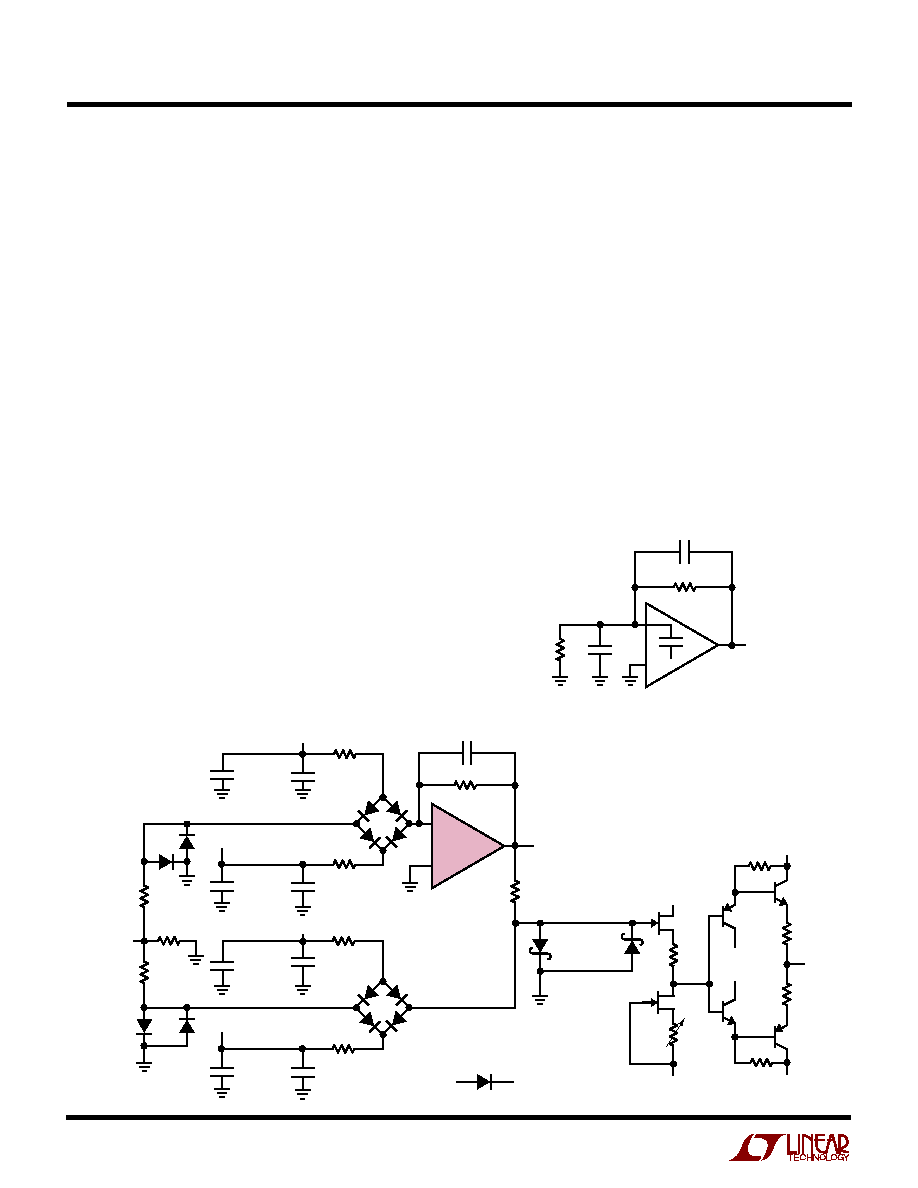
Settling time is measured in the test circuit shown. This
test configuration has two features which eliminate prob-
lems common to settling time measurments: (1) probe
capacitance is isolated from the "false summing" node,
and (2) it does not require a "flat top" input pulse since the
input pulse is merely used to steer current through the
diode bridges. For more details, please see Application
Note 10.
As with most high speed amplifiers, care should be
taken with supply decoupling, lead dress and component
placement.
When the feedback around the op amp is resistive (R
F
), a
pole will be created with R
F
, the source resistance and
capacitance (R
S
, C
S
), and the amplifier input capacitance
(C
IN
4pF). In low closed-loop gain configurations and
with R
S
and R
F
in the kilohm range, this pole can create
excess phase shift and even oscillation. A small capacitor
(C
F
) in parallel with R
F
eliminates this problem. With R
S
(C
S
+ C
IN
) = R
F
C
F
, the effect of the feedback pole is
completely removed.
0.01 DISC
+
+
+
+
+
≠
+
15V
15V
≠15V
≠15V
15k
15k
15k
15k
10k
4.7k
4.7k
10
µ
F
SOLID
TANTALUM
10
µ
F
SOLID
TANTALUM
10
µ
F
SOLID
TANTALUM
10
µ
F
SOLID TANTALUM
10pF (TYPICAL)
10k
PULSE GEN
INPUT
(5V MIN STEP)
2k
2k
0.01 DISC
0.01 DISC
0.01 DISC
50
2W
LT1055
LT1056
AMPLIFIER
UNDER
TEST
AUT OUTPUT
HP5082-8210
HEWLETT
PACKARD
15V
15V
15V
≠15V
= 1N4148
≠15V
≠15V
1/2
U440
1/2
U440
50
3
3
100
DC ZERO
2N160
2N5160
2N3866
2N3866
LT1055/56 AI04
OUTPUT
TO SCOPE
Settling Time Test Circuit
≠
+
R
S
R
F
C
F
C
S
C
IN
OUTPUT
LT1055/56 AI03
11
LT1055/LT1056
10556fb
APPLICATIO
N
S I
N
FOR
M
ATIO
N
W
U
U
U
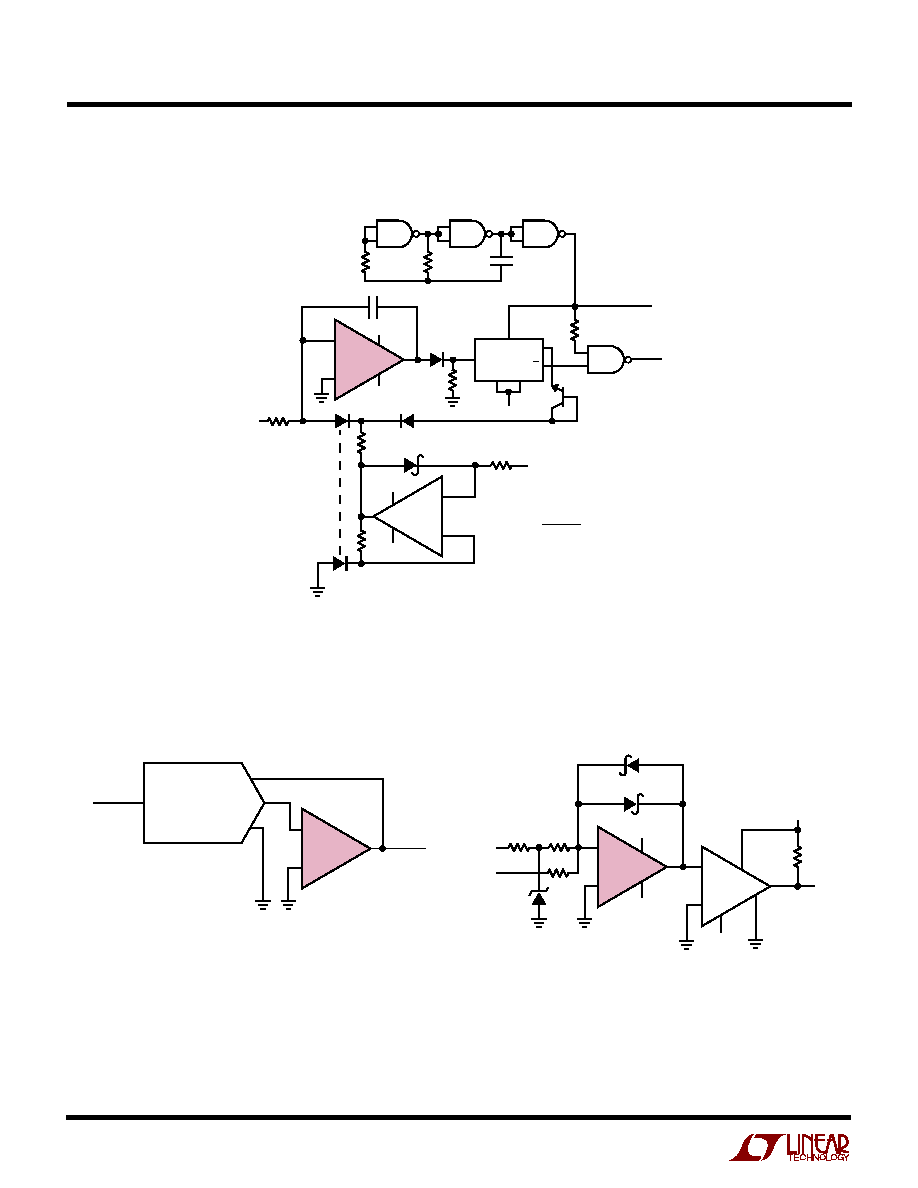
Phase Reversal Protection
Most industry standard JFET input op amps (e.g., LF155/
LF156, LF351, LF411, OP15/16) exhibit phase reversal at
the output when the negitive common mode limit at the
input is exceeded (i.e., from ≠12V to ≠15V with
±
15V
supplies). This can cause lock-up in servo systems. As
shown below, the LT1055/LT1056 does not have this
problem due to unique phase reversal protection circuitry
(Q1 on simplified schematic).
0.5ms/DIV
0.5ms/DIV
0.5ms/DIV
10V/DIV
10V/DIV
10V/DIV
LT1055/56 AI06
LT1055/56 AI07
LT1055/56 AI08
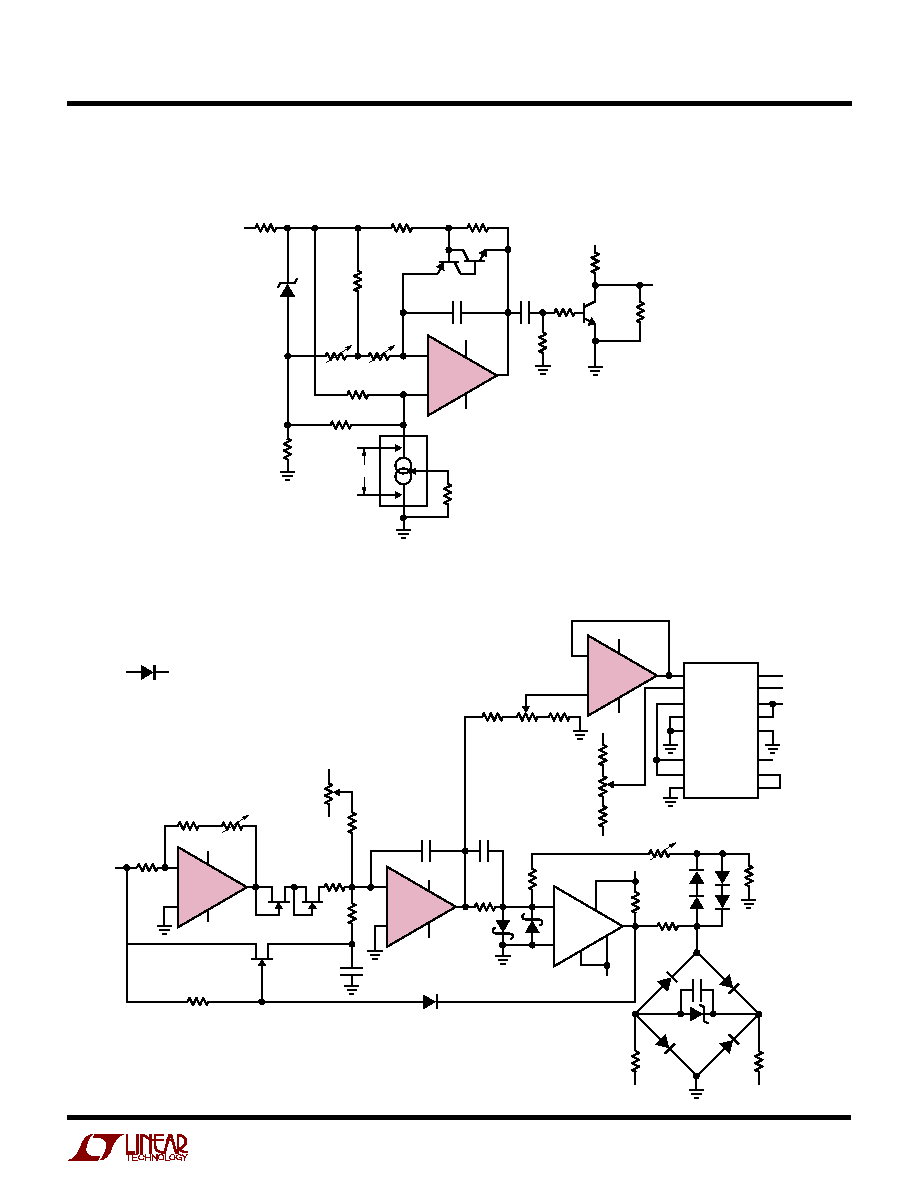
TYPICAL APPLICATIO
N
S
U
Exponential Voltage-to-Frequency Converter for Music Synthesizers
INPUT
0V TO 10V
LT1055/56 TA03
≠
+
11.3k*
EXPONENT
TRIM
2500
*
562
*
3.57k*
ZERO TRIM
15V
500k
500
*
4.7k
1.1k
10k*
3k
10k*
1k*
1k*
4.7k
2
3
4
5
6
≠15V
≠15V
7
LT1055
15V
500pF
POLYSTYRENE
6
2
3
15V
7
LM301A
15V
6
8
2N3906
2N3904
SAWTOOTH
OUTPUT
LM329
0.01
µ
F
1
4
2
3
1
1N148
13
14
15 2.2k
9
7
8
33
TEMPERATURE CONTROL LOOP
SCALE FACTOR
1V IN OCTAVE OUT
*1% METAL FILM RESISTOR
PIN NUMBERED TRANSISTORS = CA3096 ARRAY
≠
+
For ten additional applications utilizing the
LT1055 and LT1056, please see the LTC1043
data sheet and Application Note 3.
Voltage Follower with Input Exceeding the Negative
Common Mode Range
≠
+
2k
≠15V
15V
OUTPUT
2
3
4
INPUT
±
15V
SINE WAVE
7
6
LT1055/56
LT1055/56 AI05
Output
LT1055/LT1056
Output
(LF155/LF56, LF441, OP-15/OP-16)
Input
12
LT1055/LT1056
10556fb
Fast, 16-Bit Current Comparator
≠
+
≠
+
2
15V
7
6
3
15V
LT1056
4.7k
50k*
INPUT
LT1009
2.5V
100k*
4
≠15V
2
HP5082-2810
8
15V
3k
OUTPUT
1
7
4
≠15V
LT1011
3
DELAY = 250ns
* = 1% FILM RESISTOR
LT1055/56 TA06
12-Bit Charge Balance A/D Converter
≠
+
≠
+
28k
33k
14k
74C00
0.003
µ
F
CLK OUTPUT (B)
10k
OUTPUT
(A)
D
P
CL
Q
Q
CLK
74C74
1N4148
0.01
2
15V
≠15V
7
4
6
3
1N4148
1N4148
15V
10k
2N3904
249k*
0V TO 10V INPUT
COUPLE
THERMALLY
1N4148
6
33k
LM329
10k
15V
2
3
7
4
15V
≠15V
LT1055/56 TA04
LT1055
LT1001
CIRCUIT OUTPUT
RATIO
f
OUT
(A)
f
CLK
(B)
Fast "No Trims" 12-Bit Multiplying CMOS DAC Amplifier
LT1055/56 TA05
R
FEEDBACK
I
OUT1
I
OUT2
OUTPUT
REFERENCE
IN
TYPICAL 12-BIT
CMOS DAC
≠
+
LT1055
TYPICAL APPLICATIO S
U
13
LT1055/LT1056
10556fb
TYPICAL APPLICATIO S
U
Temperature-to-Frequency Converter
LT1055/56 TA07
2
3
≠15V
7
4
6
LT1055
15V
15V
560
15V
≠
+
LM329
510
820
*
6.2k*
500
0
∞
C ADJ
2k
100
∞
C
ADJ
6.2k*
1k*
1k*
2N2907
2N2222
0.01
µ
F
POLYSTYRENE
510pF
2.7k
10k
10k
4.7k
2N2222
TTL OUTPUT
0kHz TO 1kHz =
0
∞
C TO 100
∞
C
2V
LM134
137
*
*1% FILM RESISTOR
100kHz Voltage Controlled Oscillator
≠
+
≠
+
≠
+
≠
+
X1
X2
U1
U2
COM
VR
Y1
Y2
+
V
CC
W
Z1
Z2
GT
UP
≠V
+
15V
SINE OUT
2V
RMS
0kHs TO 100kHs
≠15
AD639
2
3
15V
7
6
4
≠15V
≠15V
68k
68k
10k
4.5k
22.1k
1k
LT1056
FINE
DISTORTION
TRIMS
15V
15V
15V
15V
≠15V
≠15V
≠15V
≠15V
LT1055/56 TA08
50k
10Hz
DISTORTION
TRIM
22M
POLYSTYRENE
500pF
7
4
3
2
6
LT1056
22k
15pF
HP5082-
2810
3
2
10k*
10k
1k
4.7k
4.7k
*1% FILM RESISTOR
=1N4148
FREQUENCY LINEARITY = 0.1%
FREQUENCY STABILITY = 150ppm/
∞
C
SETTLING TIME = 1.7
µ
s
DISTORTION = 0.25% AT 100kHz,
0.07% AT 10zHz
1k
5k
FREQUENCY
TRIM
LT1011
8
7
1
4
LM329
0.01
µ
F
2.5k*
10k*
5k*
2N4391
2N4391
2N4391
6
7
4
15V
≠15V
LT1056
100kHz
DISTORTION
TRIM
2k
9.09k*
0V TO 10V
INPUT
2
3
10k
20pF
14
LT1055/LT1056
10556fb
1
3
2
NULL
5
7
6
OUTPUT
NULL
≠INPUT
+
INPUT
7k
7k
J6
J7
J4
J3
J8
J5
J1
J2
Q7
Q3
Q4
Q8
Q9
Q2
Q1
Q14
Q12
Q11
Q10
Q13
Q15
Q16
400
µ
A*
(1100)
Q5
7.5pF
300
50
3k
V
+
4 V
≠
20
200
800
µ
A*
(1000)
120
µ
A*
(160)
120
µ
A*
(160)
8k
14k
14k
9pF
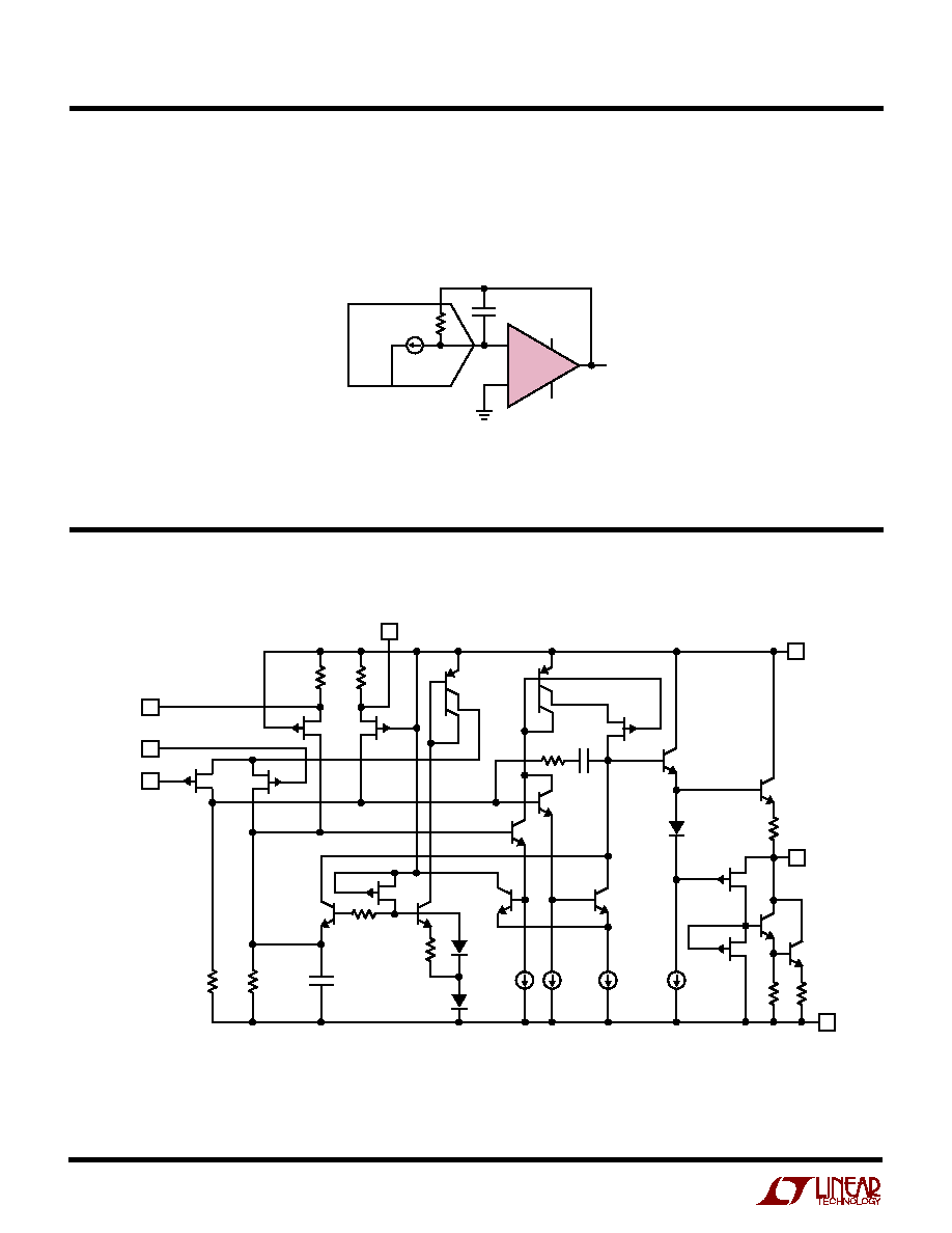
*CURRENTS AS SHOWN FOR LT1055. (X) = CURRENTS FOR LT1056.
LT1055/56 SCHM
SCHE ATIC
W
W
SI PLIFIED
TYPICAL APPLICATIO S
U
≠
+
15V
≠15V
7
4
3
2
6
LT1056
OUTPUT
0V TO 10V
C
F
= 15pF TO 33pF
SETTLING TIME TO 2mV
(0.8 LSB) = 1.5
µ
s TO 2
µ
s
0 TO 2
OR 4mA
12-BIT CURRENT OUTPUT D/A
CONVERTER (e.g., 6012,565
OR DAC-80)
C
F
LT1055/56 TA09
12-Bit Voltage Output D/A Converter
15
LT1055/LT1056
10556fb
Information furnished by Linear Technology Corporation is believed to be accurate and reliable.
However, no responsibility is assumed for its use. Linear Technology Corporation makes no represen-
tation that the interconnection of its circuits as described herein will not infringe on existing patent rights.
PACKAGE DESCRIPTIO
U
H Package
8-Lead TO-5 Metal Can (.200 Inch PCD)
(Reference LTC DWG # 05-08-1320)
N8 Package
8-Lead PDIP (Narrow .300 Inch)
(Reference LTC DWG # 05-08-1510)
N8 1098
0.100
(2.54)
BSC
0.065
(1.651)
TYP
0.045 ≠ 0.065
(1.143 ≠ 1.651)
0.130
±
0.005
(3.302
±
0.127)
0.020
(0.508)
MIN
0.018
±
0.003
(0.457
±
0.076)
0.125
(3.175)
MIN
1
2
3
4
8
7
6
5
0.255
±
0.015*
(6.477
±
0.381)
0.400*
(10.160)
MAX
0.009 ≠ 0.015
(0.229 ≠ 0.381)
0.300 ≠ 0.325
(7.620 ≠ 8.255)
0.325
+0.035
≠0.015
+0.889
≠0.381
8.255
(
)
*THESE DIMENSIONS DO NOT INCLUDE MOLD FLASH OR PROTRUSIONS.
MOLD FLASH OR PROTRUSIONS SHALL NOT EXCEED 0.010 INCH (0.254mm)
0.050
(1.270)
MAX
0.016 ≠ 0.021**
(0.406 ≠ 0.533)
0.010 ≠ 0.045*
(0.254 ≠ 1.143)
SEATING
PLANE
0.040
(1.016)
MAX
0.165 ≠ 0.185
(4.191 ≠ 4.699)
GAUGE
PLANE
REFERENCE
PLANE
0.500 ≠ 0.750
(12.700 ≠ 19.050)
0.305 ≠ 0.335
(7.747 ≠ 8.509)
0.335 ≠ 0.370
(8.509 ≠ 9.398)
DIA
0.200
(5.080)
TYP
0.027 ≠ 0.045
(0.686 ≠ 1.143)
0.028 ≠ 0.034
(0.711 ≠ 0.864)
0.110 ≠ 0.160
(2.794 ≠ 4.064)
INSULATING
STANDOFF
45
∞
TYP
H8(TO-5) 0.200 PCD 1197
LEAD DIAMETER IS UNCONTROLLED BETWEEN THE REFERENCE PLANE
AND 0.045" BELOW THE REFERENCE PLANE
FOR SOLDER DIP LEAD FINISH, LEAD DIAMETER IS
0.016 ≠ 0.024
(0.406 ≠ 0.610)
*
**
PIN 1
OBSOLETE PACKAGE
16
LT1055/LT1056
10556fb
0.016 ≠ 0.050
(0.406 ≠ 1.270)
0.010 ≠ 0.020
(0.254 ≠ 0.508)
◊
45
∞
0
∞
≠ 8
∞
TYP
0.008 ≠ 0.010
(0.203 ≠ 0.254)
SO8 1298
0.053 ≠ 0.069
(1.346 ≠ 1.752)
0.014 ≠ 0.019
(0.355 ≠ 0.483)
TYP
0.004 ≠ 0.010
(0.101 ≠ 0.254)
0.050
(1.270)
BSC
1
2
3
4
0.150 ≠ 0.157**
(3.810 ≠ 3.988)
8
7
6
5
0.189 ≠ 0.197*
(4.801 ≠ 5.004)
0.228 ≠ 0.244
(5.791 ≠ 6.197)
DIMENSION DOES NOT INCLUDE MOLD FLASH. MOLD FLASH
SHALL NOT EXCEED 0.006" (0.152mm) PER SIDE
DIMENSION DOES NOT INCLUDE INTERLEAD FLASH. INTERLEAD
FLASH SHALL NOT EXCEED 0.010" (0.254mm) PER SIDE
*
**
LT/CPI 0302 1.5K REV B ∑ PRINTED IN USA
©
LINEAR TECHNOLOGY CORPORATION 1994
Linear Technology Corporation
1630 McCarthy Blvd., Milpitas, CA 95035-7417
(408) 432-1900
q
FAX: (408) 434-0507
q
www.linear.com
10k
10k
100pF
LT1055/56 TA10
≠
+
7
4
3
2
6
LT1055
10k
INPUT
1N965
1
µ
F
510
330
125V
2N5415
50k
50k
1M
1M
1N4148
1N4148
2N2222
2N2907
1k
1k
2N3440
27
27
OUTPUT
2N5415
2N3440
330
510
1N965
1
µ
F
≠125V
33pF
100k
10k
±
25mA OUTPUT
HEAT SINK OUTPUT
TRANSISTORS
±
120V Output Precision Op Amp
TYPICAL APPLICATIO
U
RELATED PARTS
PART NUMBER
DESCRIPTION
COMMENTS
LT1122
Fast Settling JFET Op Amp
340ns Settling Time, GBW = 14MHz, SR = 60V/
µ
s
LT1792
Low Noise JFET Op Amp
e
n
= 6nV/
Hz Max at f = 1kHz
PACKAGE DESCRIPTIO
U