 | –≠–ª–µ–∫—Ç—Ä–æ–Ω–Ω—ã–π –∫–æ–º–ø–æ–Ω–µ–Ω—Ç: LT1071HVM | –°–∫–∞—á–∞—Ç—å:  PDF PDF  ZIP ZIP |

10701fe
1
LT1070/LT1071
FEATURES
APPLICATIO S
U
DESCRIPTIO
U
TYPICAL APPLICATIO
U
5A and 2.5A High Efficiency
Switching Regulators
s
Wide Input Voltage Range: 3V to 60V
s
Low Quiescent Current: 6mA
s
Internal 5A Switch (2.5A for LT1071)
s
Very Few External Parts Required
s
Self Protected Against Overloads
s
Operates in Nearly All Switching Topologies
s
Shutdown Mode Draws Only 50
µ
A Supply Current
s
Flyback Regulated Mode Has Fully Floating Outputs
s
Comes in Standard 5-Pin TO-220 Package
s
Can be Externally Synchronized (Consult Factory)
The LT
Æ
1070/LT1071 are monolithic high power switch-
ing regulators. They can be operated in all standard switch-
ing configurations including buck, boost, flyback, for-
ward, inverting and "Cuk". A high current, high efficiency
switch is included on the die along with all oscillator,
control and protection circuitry. Integration of all func-
tions allows the LT1070/LT1071 to be built in a standard
5-pin T0-220 power package. This makes it extremely
easy to use and provides "bust proof" operation similar to
that obtained with 3-pin linear regulators.
The LT1070/LT1071 operate with supply voltages from 3V
to 60V, and draw only 6mA quiescent current. They can
deliver load power up to 100W with no external power
devices. By utilizing current mode switching techniques,
they provide excellent AC and DC load and line regulation.
The LT1070/LT1071 have many unique features not found
even on the vastly more difficult to use low power control
chips presently available. They use adaptive antisat switch
drive to allow very wide ranging load currents with no loss
in efficiency. An externally activated shutdown mode
reduces total supply current to 50
µ
A typical for standby
operation. Totally isolated and regulated outputs can be
generated by using the optional "flyback regulation mode"
built into the LT1070/LT1071, without the need for
optocouplers or extra transformer windings.
USER NOTE:
This data sheet is only intended to provide specifications, graphs and a general functional
description of the LT1070/LT1071. Application circuits are included to show the capability of the
LT1070/LT1071. A complete design manual (AN19) should be obtained to assist in developing new
designs. This manual contains a comprehensive discussion of both the LT1070 and the external
components used with it, as well as complete formulas for calculating the values of these
components. The manual can also be used for the LT1071 by factoring in the lower switch current
rating. A second Application Note, AN25, which details off-line applications is available.
+
R1
10.7k
1%
R2
1.24k
1%
1070/71 TA01
12V
1A
R3
1k
C1
1
µ
F
C2
1000
µ
F
+
C3*
100
µ
F
L1**
150
µ
H
D1
5V
V
SW
V
C
V
IN
LT1070
GND
FB
C3
100
µ
F
L2
10
µ
H
OUTPUT
FILTER
*
**
REQUIRED IF INPUT LEADS
2"
PULSE ENGINEERING 92113
INPUT VOLTAGE (V)
0
POWER (W)**
60
80
100
40
1070/71 TA02
40
20
0
10
20
30
50
BOOST
BUCK/BOOST
V
O
= 30V
FLYBACK
ISOLATED
BUCK/BOOST
V
O
= 5V
ROUGH GUIDE ONLY. BUCK MODE P
OUT
= 5A ∑ V
OUT
.
SPECIAL TOPOLOGIES DELIVER MORE POWER
DIVIDE VERTICAL POWER SCALE BY 2 FOR LT1071
*
**
Maximum Output Power*
Boost Converter (5V to 12V)
s
Logic Supply 5V at 10A
s
5V Logic to
±
15V Op Amp Supply
s
Off-Line Converter Up to 200W
s
Battery Upconverter
s
Power Inverter (+ to ≠) or (≠ to +)
s
Fully Floating Multiple Outputs
s
For Lower Current Applications, See the LT1072
, LTC and LT are registered trademarks of Linear Technology Corporation.
2
LT1070/LT1071
10701fe
SYMBOL
PARAMETER
CONDITIONS
MIN
TYP
MAX
UNITS
V
REF
Reference Voltage
Measured at Feedback Pin, V
C
= 0.8V
1.224
1.244
1.264
V
q
1.214
1.244
1.274
V
I
B
Feedback Input Current
V
FB
= V
REF
350
750
nA
q
1100
nA
g
m
Error Amplifier Transconductance
I
C
=
±
25
µ
A
3000
4400
6000
µ
mho
q
2400
7000
µ
mho
Error Amplifier Source or Sink Current
V
C
= 1.5V
150
200
350
µ
A
q
120
400
µ
A
Error Amplifier Clamp Voltage
Hi Clamp, V
FB
= 1V
1.80
2.30
V
Lo Clamp, V
FB
= 1.5V
0.25
0.38
0.52
V
Reference Voltage Line Regulation
3V
V
IN
V
MAX
, V
C
= 0.8V
q
0.03
%/V
A
V
Error Amplifier Voltage Gain
0.9V
V
C
1.4V
500
800
V/V
Minimum Input Voltage
q
2.6
3.0
V
I
Q
Supply Current
3V
V
IN
V
MAX
, V
C
= 0.6V
6
9
mA
Control Pin Threshold
Duty Cycle = 0
0.8
0.9
1.08
V
q
0.6
1.25
V
Normal/Flyback Threshold on Feedback Pin
0.4
0.45
0.54
V
ABSOLUTE
M
AXI
M
U
M
RATINGS
W
W
W
U
Supply Voltage
LT1070/LT1071 (Note 2) .................................... 40V
LT1070HV/LT1071HV (Note 2) .......................... 60V
Switch Output Voltage
LT1070/LT1071 .................................................. 65V
LT1070HV/LT1071HV ........................................ 75V
Feedback Pin Voltage (Transient, 1ms) ................
±
15V
Operating Junction Temperature Range
Commercial (Operating) ....................... 0
∞
C to 100
∞
C
Commercial (Short Circuit)................... 0
∞
C to 125
∞
C
Industrial ......................................... ≠ 40
∞
C to 125
∞
C
Military (OBSOLETE) ................. ≠ 55
∞
C to 150
∞
C
Storage Temperature Range ................ ≠ 65
∞
C to 150
∞
C
Lead Temperature (Soldering, 10 sec)................. 300
∞
C
PACKAGE/ORDER I
N
FOR
M
ATIO
N
W
U
U
ORDER PART
NUMBER
LT1070CK
LT1070HVCK
LT1070HVMK
LT1070IK
LT1070MK
LT1071CK
LT1071HVCK
LT1071HVMK
LT1071MK
ORDER PART
NUMBER
LT1070CT
LT1070HVCT
LT1070HVIT
LT1070IT
LT1071CT
LT1071HVCT
LT1071HVIT
LT1071IT
T
JMAX
= 100
∞
C,
JA
= 35
∞
C/ W, Q
JC
= 2
∞
C (LT1070C, I)
T
JMAX
= 150
∞
C,
JA
= 35
∞
C/ W, Q
JC
= 2
∞
C (LT1070M)
T
JMAX
= 100
∞
C,
JA
= 35
∞
C/ W, Q
JC
= 4
∞
C (LT1071C, I)
T
JMAX
= 150
∞
C,
JA
= 35
∞
C/ W, Q
JC
= 4
∞
C (LT1071M)
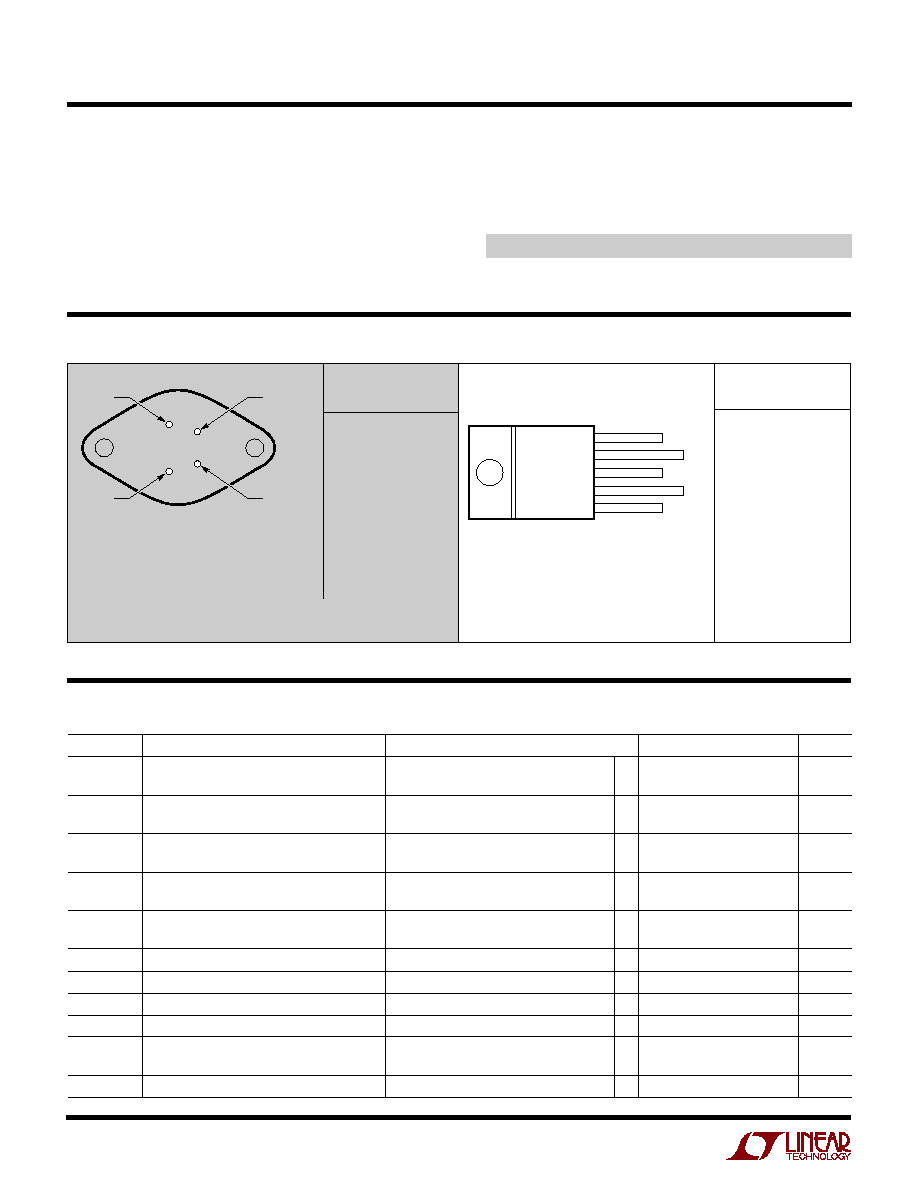
2
4
1
3
V
SW
V
C
FB
CASE
IS GND
V
IN
K PACKAGE
4-LEAD TO-3 METAL CAN
BOTTOM VIEW
T
JMAX
= 100
∞
C,
JA
= 75
∞
C/ W, Q
JC
= 2
∞
C (LT1070C, I)
T
JMAX
= 100
∞
C,
JA
= 75
∞
C/ W, Q
JC
= 4
∞
C (LT1071C)
T PACKAGE
5-LEAD PLASTIC TO-220
V
IN
V
SW
GND
FB
V
C
FRONT VIEW
5
4
3
2
1
ELECTRICAL CHARACTERISTICS
(Note 1)
Consult LTC Marketing for parts specified with wider operating temperature ranges.
OBSOLETE PACKAGE
Consider the T5 Package for Alternate Source
The
q
denotes the specifications which apply over the full operating temperature
range, otherwise specifications are at T
A
= 25
∞
C. V
IN
= 15V, V
C
= 0.5V, V
FB
= V
REF
, output pin open unless otherwise specified.
10701fe
3
LT1070/LT1071
ELECTRICAL CHARACTERISTICS
SYMBOL
PARAMETER
CONDITIONS
MIN
TYP
MAX
UNITS
V
FB
Flyback Reference Voltage
I
FB
= 50
µ
A
15
16.3
17.6
V
q
14
18.0
V
Change in Flyback Reference Voltage
0.05
I
FB
1mA
4.5
6.8
8.5
V
Flyback Reference Voltage Line Regulation
I
FB
= 50
µ
A, 3V
V
IN
V
MAX
(Note 3)
0.01
0.03
%/V
Flyback Amplifier Transconductance (g
m
)
I
C
=
±
10
µ
A
150
300
650
µ
mho
Flyback Amplifier Source and Sink Current
V
C
= 0.6V, I
FB
= 50
µ
A (Source)
q
15
32
70
µ
A
V
C
= 0.6V, I
FB
= 50
µ
A (Sink)
q
25
40
70
µ
A
B
V
Output Switch Breakdown Voltage
3V
V
IN
V
MAX
,
I
SW
= 1.5mA
(LT1070/LT1071)
q
65
90
V
(LT1070HV/LT1071HV)
q
75
90
V
V
SAT
Output Switch "On" Resistance (Note 4)
LT1070
q
0.15
0.24
LT1071
q
0.30
0.50
Control Voltage to Switch Current
LT1070
8
A/V
Transconductance
LT1071
4
A/V
I
LIM
Switch Current Limit (LT1070)
Duty Cycle
50%, T
J
25
∞
C
q
5
10
A
Duty Cycle
50%, T
J
< 25
∞
C
q
5
11
A
Duty Cycle = 80% (Note 5)
q
4
10
A
Switch Current Limit (LT1071)
Duty Cycle
50%, T
J
25
∞
C
q
2.5
5.0
A
Duty Cycle
50%, T
J
< 25
∞
C
q
2.5
5.5
A
Duty Cycle = 80% (Note 5)
q
2.0
5.0
A
I
IN
Supply Current Increase During
25
35
mA/A
I
SW
Switch "On" Time
f
Switching Frequency
35
40
45
kHz
q
33
47
kHz
DC (Max)
Maximum Switch Duty Cycle
90
92
97
%
Flyback Sense Delay Time
1.5
µ
s
Shutdown Mode Supply Current
3V
V
IN
V
MAX
, V
C
= 0.05V
100
250
µ
A
Shutdown Mode Threshold Voltage
3V
V
IN
V
MAX
100
150
250
mV
q
50
300
mV
Note 1: Absolute Maximum Ratings are those values beyond which the life of
a device may be impaired.
Note 2: Minimum switch "on" time for the LT1070/LT1071 in current limit is
1
µ
s. This limits the maximum input voltage during short-circuit conditions,
in the buck and inverting modes only, to
35V. Normal (unshorted) conditions
are not affected. Mask changes are being implemented which will reduce
minimum "on" time to
1
µ
s, increasing maximum short-circuit input voltage
above 40V. If the present LT1070/LT1071 (contact factory for package date
code) is being operated in the buck or inverting mode at high input voltages
and short-circuit conditions are expected, a resistor must be placed in series
with the inductor, as follows:
The value of the resistor is given by:
R =
≠ R
L
t ∑ f ∑ V
IN
≠ V
F
I
LIMIT
t = Minimum "on" time of LT1070/LT1071 in current limit,
1
µ
s
f = Operating frequency (40kHz)
V
F
= Forward voltage of external catch diode at I
LIMIT
I
LIMIT
= Current limit of LT1070 (
8A), LT1071 (
4A)
R
L
= Internal series resistance of inductor
Note 3: V
MAX
= 55V for LT1070HV and LT1071HV to avoid switch
breakdown.
Note 4: Measured with V
C
in hi clamp, V
FB
= 0.8V. I
SW
= 4A for LT1070
and 2A for LT1071.
Note 5: For duty cycles (DC) between 50% and 80%, minimum
guaranteed switch current is given by I
LIM
= 3.33 (2 ≠ DC) for the
LT1070 and I
LIM
= 1.67 (2 ≠ DC) for the LT1071.
The
q
denotes the specifications which apply over the full operating temperature
range, otherwise specifications are at T
A
= 25
∞
C. V
IN
= 15V, V
C
= 0.5V, V
FB
= V
REF
, output pin open unless otherwise specified.
4
LT1070/LT1071
10701fe
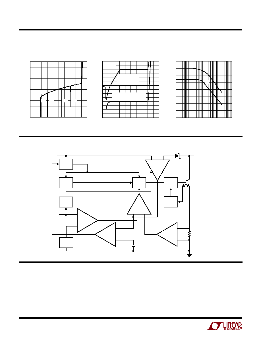
TYPICAL PERFOR
M
A
N
CE CHARACTERISTICS
U
W
Switch Current Limit vs Duty Cycle
DUTY CYCLE (%)
0
SWITCH CURRENT (A)
16
14
12
10
8
6
4
2
0
80
1070/71 G01
20
40
60
100
70
10
30
50
90
FOR LT1071, DIVIDE
VERTICAL SCALE BY 2
≠ 55
∞
C
125
∞
C
25
∞
C
Flyback Blanking Time
JUNCTION TEMPERATURE (
∞
C)
≠75
1.0
TIME (
µ
s)
1.2
1.6
1.8
2.0
≠ 25
25
50
150
1070/71 G03
1.4
≠ 50
0
75 100 125
2.2
JUNCTION TEMPERATURE (
∞
C)
≠75
90
DUTY CYCLE (%)
91
93
94
95
≠ 25
25
50
150
1070/71 G02
92
≠ 50
0
75 100 125
96
Maximum Duty Cycle
Minimum Input Voltage
TEMPERATURE (
∞
C)
≠75
2.3
MINIMUM INPUT VOLTAGE (V) 2.4
2.6
2.7
2.8
≠ 25
25
50
150
1070/71 G04
2.5
≠ 50
0
75 100 125
2.9
SWITCH CURRENT = 5A
SWITCH CURRENT = 0A
Switch Saturation Voltage
SWITCH CURRENT (A)
0
SWITCH SATURATION VOLTAGE (V)
0.8
1.2
8
1070/71 G05
0.4
0
1.0
25
∞
C
1.4
0.6
0.2
2
4
6
1
3
5
7
1.6
FOR LT1071, DIVIDE
CURRENT BY 2
100
∞
C
≠ 55
∞
C
150
∞
C
TEMPERATURE (
∞
C)
≠ 75
FLYBACK VOLTAGE (V)
19
20
21
125
1070/71 G06
18
17
15
≠ 25
25
75
≠ 50
150
0
50
100
16
23
22
R
FEEDBACK
= 500
R
FEEDBACK
= 1k
R
FEEDBACK
= 10k
Line Regulation
Feedback Bias Current
vs Temperature
INPUT VOLTAGE (V)
0
≠ 5
REFERENCE VOLTAGE CHANGE (mV)
≠ 3
≠1
1
10
20
30
40
1070/71 G07
50
3
5
≠ 4
≠ 2
0
2
4
60
T
J
= 150
∞
C
T
J
= 25
∞
C
T
J
= ≠ 55
∞
C
TEMPERATURE (
∞
C)
≠ 75
FEEDBACK BIAS CURRENT (nA)
600
500
400
300
200
100
0
125
1070/71 G09
≠ 25
25
75
≠ 50
150
0
50
100
800
700
Reference Voltage
vs Temperature
TEMPERATURE (
∞
C)
≠ 75
REFERENCE VOLTAGE (V)
SWITCHING FREQUENCY (kHz)
1.246
1.244
1.242
1.240
1.238
1.236
1.234
125
1070/71 G08
≠ 25
25
75
≠ 50
150
0
50
100
1.250
1.248
40
39
38
37
36
35
34
42
41
SWITCHING
FREQUENCY
REFERENCE
V0LTAGE
10701fe
5
LT1070/LT1071
TYPICAL PERFOR
M
A
N
CE CHARACTERISTICS
U
W
Supply Current vs Supply Voltage
(Shutdown Mode)
Driver Current* vs Switch Current
SWITCH CURRENT (A)
0
DRIVER CURRENT (mA)
160
140
120
100
80
60
40
20
0
4
1070/71 G10
1
*
2
3
5
T
J
25
∞
C
AVERAGE LT1070 POWER SUPPLY CURRENT IS
FOUND BY MULTIPLYING DRIVER CURRENT BY
DUTY CYCLE, THEN ADDING QUIESCENT CURRENT
T
J
= ≠ 55
∞
C
SUPPLY VOLTAGE (V)
0
SUPPLY CURRENT (
µ
A)
60
80
100
30
50
1070/71 G12
40
20
0
10
20
40
120
140
160
60
T
J
= 25
∞
C
V
C
= 50mV
V
C
= 0V
Supply Current vs Input Voltage*
INPUT VOLTAGE (V)
0
6
INPUT CURRENT (mA)
8
10
12
10
20
30
*
40
1070/71 G11
50
14
UNDER VERY LOW OUTPUT CURRENT
CONDITIONS, DUTY CYCLE FOR MOST
CIRCUITS WILL APPROACH 10% OR LESS
16
7
9
11
13
15
60
T
J
= 25
∞
C
I
SWITCH
10mA
90% DUTY CYCLE
50% DUTY CYCLE
0% DUTY CYCLE
10% DUTY CYCLE
Feedback Pin Clamp Voltage
Shutdown Thresholds
TEMPERATURE (
∞
C)
≠ 75
V
C
PIN VOLTAGE (mV)
V
C
PIN CURRENT (
µ
A)
300
250
200
150
100
50
0
125
1070/71 G16
≠ 25
25
75
≠ 50
150
0
50
100
400
350
≠300
≠250
≠200
≠150
≠100
≠ 50
0
≠ 400
≠350
V
C
VOLTAGE IS REDUCED UNTIL
REGULATOR CURRENT DROPS
BELOW 300
µ
A
VOLTAGE
CURRENT
(OUT OF V
C
PIN)
FEEDBACK CURRENT (mA)
0
FEEDBACK VOLTAGE (mV)
300
400
500
0.8
1070/71 G18
200
100
250
350
450
150
50
0
0.2
0.4
0.6
0.1
0.9
0.3
0.5
0.7
1.0
≠ 55
∞
C
25
∞
C
150
∞
C
TEMPERATURE (
∞
C)
≠75
IDLE SUPPLY CURRENT (mA)
7
9
11
125
1070/71 G14
5
3
6
8
10
4
2
1
≠25
25
75
≠ 50
150
0
50
100
V
C
= 0.6V
V
SUPPLY
= 60V
V
SUPPLY
= 3V
Idle Supply Current
vs Temperature
Normal/Flyback Mode Threshold
on Feedback Pin
TEMPERATURE (
∞
C)
≠50
400
FEEDBACK PIN VOLTAGE (mV)
FEEDBACK PIN CURRENT (
µ
A)
410
430
440
450
500
470
0
50
75
1070/71 G13
420
480
490
460
≠ 4
≠ 6
≠10
≠12
≠14
≠24
≠18
≠ 8
≠20
≠22
≠16
≠25
25
100 125
150
FEEDBACK PIN VOLTAGE
(AT THRESHOLD)
FEEDBACK PIN CURRENT
(AT THRESHOLD)
Error Amplifier Transconductance
TEMPERATURE (
∞
C)
≠75
TRANSCONDUCTANCE (
µ
mho)
3000
4000
5000
125
1070/71 G14
2000
1000
2500
3500
4500
1500
500
0
≠25
25
75
≠ 50
150
0
50
100
g
m
=
(V
C
PIN)
(FB PIN)
I
V
Shutdown Mode Supply Current
V
C
PIN VOLTAGE (mV)
0
SUPPLY CURRENT (
µ
A)
120
160
200
80
1070/71 G14
80
40
100
140
180
60
20
0
20
40
60
10
90
30
50
70
100
T
J
= 150
∞
C
≠ 55
∞
C
T
J
125
∞
C
6
LT1070/LT1071
10701fe
TYPICAL PERFOR
M
A
N
CE CHARACTERISTICS
U
W
voltage is obtained by using the output of a voltage
sensing error amplifier to set current trip level. This
technique has several advantages. First, it has immediate
response to input voltage variations, unlike ordinary
switchers which have notoriously poor line transient
response. Second, it reduces the 90
∞
phase shift at
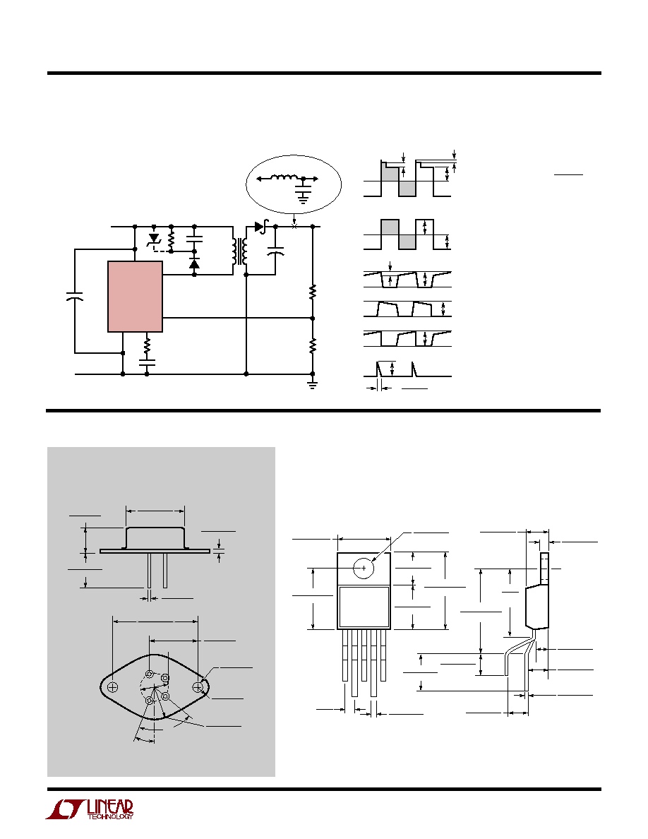
The LT1070/LT1071 is a current mode switcher. This
means that switch duty cycle is directly controlled by
switch current rather than by output voltage. Referring to
the Block Diagram, the switch is turned "on" at the start
of each oscillator cycle. It is turned "off" when switch
current reaches a predetermined level. Control of output
OPERATIO
N
U
Switch "Off" Characteristics
SWITCH VOLTAGE (V)
0
SWITCH CURRENT (
µ
A)
600
800
1000
80
1070/71 G19
400
200
500
700
900
300
100
0
20
40
60
10
90
30
50
70
100
V
SUPPLY
=
3V
15V
40V
55V
FREQUENCY (Hz)
1000
TRANSCONDUCTANCE (
µ
mho)
PHASE (
∞
)
3000
4000
6000
7000
1k
100k
1M
10M
1070/71 G21
≠1000
10k
5000
2000
0
150
90
60
0
≠ 30
210
30
120
180
g
m
Transconductance of Error
Amplifier
V
C
Pin Characteristics
V
C
PIN VOLTAGE (V)
0
≠ 400
V
C
PIN CURRENT (
µ
A)
≠ 300
≠ 200
≠100
300
100
0.5
1.0
200
0
1.5
2.0
2.5
1070/71 G20
V
FB
= 1.5V
(CURRENT INTO
V
C
PIN)
V
FB
= 0.8V
(CURRENT OUT OF V
C
PIN)
T
J
= 25
∞
C
BLOCK DIAGRA
M
W
≠
+
≠
+
ERROR
AMP
CURRENT
AMP
0.02
(0.04
LT1071)
SHUTDOWN
CIRCUIT
MODE
SELECT
40kHz
OSC
LOGIC
DRIVER
ANTISAT
16V
5A, 75V
SWITCH
V
IN
FB
V
C
COMP
GAIN
6
0.15V
1070/71 BD
1.24V
REF
2.3V
REG
FLYBACK
ERROR
AMP
SWITCH
OUT
10701fe
7
LT1070/LT1071
OPERATIO
N
U
midfrequencies in the energy storage inductor. This
greatly simplifies closed-loop frequency compensation
under widely varying input voltage or output load condi-
tions. Finally, it allows simple pulse-by-pulse current
limiting to provide maximum switch protection under
output overload or short-circuit conditions. A low drop-
out internal regulator provides a 2.3V supply for all
internal circuitry of the LT1070/LT1071. This low drop-
out design allows input voltage to vary from 3V to 60V
with virtually no change in device performance. A 40kHz
oscillator is the basic clock for all internal timing. It turns
"on" the output switch via the logic and driver circuitry.
Special adaptive antisat circuitry detects onset of satura-
tion in the power switch and adjusts driver current
instantaneously to limit switch saturation. This mini-
mizes driver dissipation and provides very rapid turn-off
of the switch.
A 1.2V bandgap reference biases the positive input of the
error amplifier. The negative input is brought out for
output voltage sensing. This feedback pin has a second
function; when pulled low with an external resistor, it
programs the LT1070/LT1071 to disconnect the main
error amplifier output and connects the output of the
flyback amplifier to the comparator input. The LT1070/
LT1071 will then regulate the value of the flyback pulse
with respect to the supply voltage. This flyback pulse is
directly proportional to output voltage in the traditional
transformer coupled flyback topology regulator. By regu-
lating the amplitude of the flyback pulse, the output
voltage can be regulated with no direct connection be-
tween input and output. The output is fully floating up to
the breakdown voltage of the transformer windings.
Multiple floating outputs are easily obtained with addi-
tional windings. A special delay network inside the LT1070/
LT1071 ignores the leakage inductance spike at the
leading edge of the flyback pulse to improve output
regulation.
The error signal developed at the comparator input is
brought out externally. This pin (V
C
) has four different
functions. It is used for frequency compensation, current
limit adjustment, soft starting and total regulator shut-
down. During normal regulator operation this pin sits at
a voltage between 0.9V (low output current) and 2.0V
(high output current). The error amplifiers are current
output (g
m
) types, so this voltage can be externally
clamped for adjusting current limit. Likewise, a capacitor
coupled external clamp will provide soft start. Switch
duty cycle goes to zero if the V
C
pin is pulled to ground
through a diode, placing the LT1070/LT1071 in an idle
mode. Pulling the V
C
pin below 0.15V causes total
regulator shutdown, with only 50
µ
A supply current for
shutdown circuitry biasing. See AN19 for full application
details.
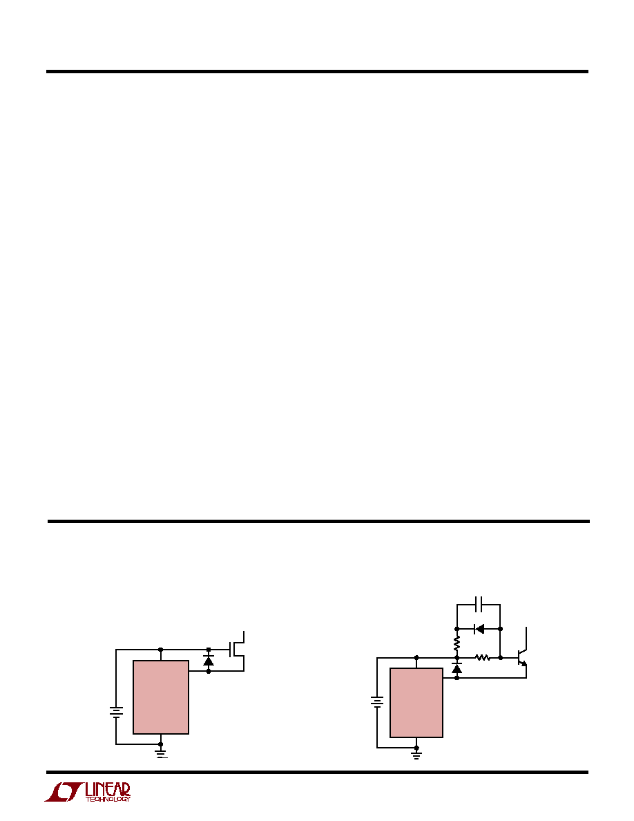
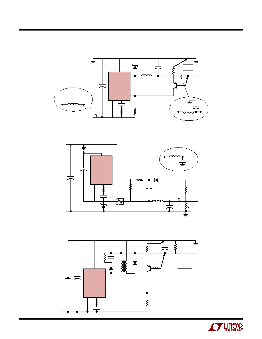
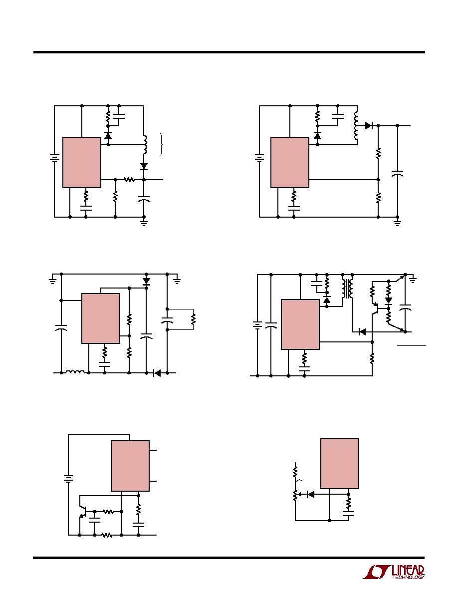
TYPICAL APPLICATIO
N
S
U
(Note that maximum output currents are divided by 2 for the LT1071)
R1*
R2**
1070/71 TA16
D1
SETS I
B(ON)
SETS I
B(OFF)
*
**
D2
C1
V
SW
V
IN
LT1070/LT1071
GND
Q1
Driving High Voltage NPN
Driving High Voltage FET (for Off-Line
Applications, See AN25)
1070/71 TA03
1070/71 TA03
10V
TO
20V
D1
V
SW
G
D
S
Q1
V
IN
LT1070/LT1071
GND
+
8
LT1070/LT1071
10701fe
TYPICAL APPLICATIO
N
S
U
(Note that maximum output currents are divided by 2 for the LT1071)
Negative Current Boosted Buck Converter
1070/71 TA13
R3
R2
1.24k
Q1
2N3906
R4
12k
C2
C3
R1
MINIMUM
LOAD = 10mA
≠ V
OUT
5V
10A
D1
T1
1:N
R5
∑
∑
C1
V
SW
V
C
V
IN
≠ V
IN
LT1070
GND
FB
+
+
V
OUT
≠ 0.6V
1mA
R1 =
1070/71 TA12
R3
R2
1.24k
*
**
REQUIRED IF INPUT LEADS
2"
PULSE ENGINEERING 92113
Q1
2N3906
R1
4.64k
C1
C2
1000
µ
F
C3
100
µ
F
V
IN
≠ 20V
≠ 5.2V
4.5A
D1
L1**
200
µ
H
V
SW
V
C
V
IN
LT1070
GND
OPTIONAL INPUT
FILTER
FB
LOAD
C4
200
µ
F
L2
4
µ
H
OPTIONAL
OUTPUT
FILTER
+
+
+
L3
Negative Buck Converter
Positive Buck Converter
R2
1.24k
R4
10
100mA
MINIMUM
1070/71 TA14
5V
4.5A
R3
470
C1
1
µ
F
D1
r
+
C3
2.2
µ
F
+
C5*
100
µ
F
+
C2
1
µ
F
+
C4
1000
µ
F
L1**
100
µ
H
V
SW
V
C
V
IN
V
IN
LT1070
R1
3.74k
D2
1N914
GND
FB
D3
L2
4
µ
H
C5
200
µ
F
OPTIONAL
OUTPUT
FILTER
*
**
REQUIRED IF INPUT LEADS
2"
PULSE ENGINEERING 92112
10701fe
9
LT1070/LT1071
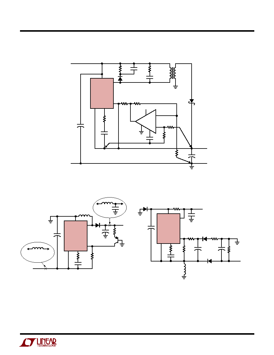
TYPICAL APPLICATIO
N
S
U
(Note that maximum output currents are divided by 2 for the LT1071)
Positive Current Boosted Buck Converter
R3
680
C1
0.33
µ
F
200pF
*REQUIRED IF INPUT LEADS
2"
R4
1.24k
C2
5000
µ
F
V
OUT
5V
10A
V
IN
28V
R1
5k
V
SW
∑
∑
V
IN
C3
0.47
µ
F
C6
0.002
µ
F
D2
470
2W
1:N
N
0.25
LT1070
GND
V
C
FB
1070/71 TA19
R6
470
≠
+
COMP
LM308
V
IN
R2
1k
R7
1.24k
R5
5k
V
≠
7
D1
2
3
8
4
6
V
+
+
C5*
100
µ
F
+
Positive to Negative Buck/Boost Converter
+
R1
11.3k
1070/71 TA05
V
OUT
12V
2A
V
IN
≠ 12V
R3
2.2k
C1
0.22
µ
F
R2
1.24k
*
**
REQUIRED IF INPUT LEADS
2"
PULSE ENGINEERING 92113
C2
1000
µ
F
+
C4*
100
µ
F
L1**
150
µ
H
Q1
D1
V
SW
V
C
V
IN
LT1070
GND
FB
C3
L2
OPTIONAL
OUTPUT
FILTER
L3
OPTIONAL
INPUT
FILTER
+
R6
470
1070/71 TA09
V
IN
10V TO 30V
*
**
REQUIRED IF INPUT LEADS
2"
PULSE ENGINEERING 92113
TO AVOID START-UP
PROBLEMS FOR INPUT
VOLTAGES BELOW 10V,
CONNECT ANODE OF D3
TO V
IN
AND REMOVE R5.
C1 MAY BE REDUCED FOR
LOWER OUTPUT CURRENTS.
C1
(500
µ
F)(I
OUT
) FOR 5V
OUTPUTS, REDUCE R3 TO
1.5k, INCREASE C2 TO 0.3
µ
F
AND REDUCE R6 TO 100
.
V
OUT
≠ 12V
2A
R3
5k
R2
1.24k
C1
0.1
µ
F
C5*
100
µ
F
C3
2
µ
F
+
C4
5
µ
F
+
C1
1000
µ
F
L1**
200
µ
H
V
SW
V
C
V
IN
LT1070
R5
470
1W
D3
1N4001
R1
10.7k
R4
47
D2
1N914
D1
GND
FB
Negative to Positive Buck/Boost Converter
10
LT1070/LT1071
10701fe
TYPICAL APPLICATIO
N
S
U
(Note that maximum output currents are divided by 2 for the LT1071)
Current Boosted Boost Converter
+
R4
1070/71 TA11
R3
R2
1.24k
R1
27k
C2
C3
I
N
C1
V
OUT
28V
4A
D2
D1
V
SW
V
C
V
IN
LT1070
GND
V
IN
16V TO 24V
FB
+
R1
27k
R
O
(MINIMUM
LOAD)
R2
1.24k
1070/71 TA15
R3
3.3k
C2
0.22
µ
F
C3
10
µ
F
+
+
C1
1000
µ
F
+
C4*
470
µ
F
V
IN
≠15V
V
OUT
≠28V
1A
L1
200
µ
H
D2
D1
V
SW
V
C
V
IN
LT1070
GND
FB
*REQUIRED IF INPUT LEADS
2"
+
R4
680
1W
1070/71 TA10
1
L1
N = 5
TOTAL
INDUCTANCE = 4mH
INTERLEAVE PRIMARY
AND SECONDARY FOR
LOW LEAKAGE
INDUCTANCE
R3
10k
R2
1.24k
R1
98k
C2
0.047
µ
F
C3
0.68
µ
F
C1
200
µ
F
V
OUT
100V
300mA
D2
D1
V
SW
V
C
V
IN
LT1070
GND
V
IN
15V
FB
+
Voltage Boosted Boost Converter
Negative Boost Regulator
Negative Input/Negative Output Flyback Converter
+
R5
R4
1.24k
C2
V
SW
Q1
2N3906
∑
∑
V
IN
C3
C1
≠ V
OUT
1070/71 TA17
R6
R1*
T1
1:N
LT1070/LT1071
GND
V
C
FB
≠ V
IN
R3
1k
R2
5k
+
*R1 =
V
OUT
≠ 1.6V
200
µ
A
External Current Limit
External Current Limit
1070/71 TA04
LT1070/LT1071
V
C
GND
D1
V
X
R1
500
R2
= 2V
1070/71 TA06
R2
V
IN
R1
1k
C2
C1
1000pF
NOTE THAT THE LT1070/LT1071
GND PIN IS NO LONGER COMMON
TO V
IN
≠
V
SW
V
C
R
S
V
IN
LT1070/LT1071
GND
FB
+
Q1
10701fe
11
LT1070/LT1071
Information furnished by Linear Technology Corporation is believed to be accurate and reliable.
However, no responsibility is assumed for its use. Linear Technology Corporation makes no represen-
tation that the interconnection of its circuits as described herein will not infringe on existing patent rights.
TYPICAL APPLICATIO
N
S
U
(Note that maximum output currents are divided by 2 for the LT1071)
T5 (TO-220) 0399
0.028 ≠ 0.038
(0.711 ≠ 0.965)
0.067
(1.70)
0.135 ≠ 0.165
(3.429 ≠ 4.191)
0.700 ≠ 0.728
(17.78 ≠ 18.491)
0.045 ≠ 0.055
(1.143 ≠ 1.397)
0.095 ≠ 0.115
(2.413 ≠ 2.921)
0.013 ≠ 0.023
(0.330 ≠ 0.584)
0.620
(15.75)
TYP
0.155 ≠ 0.195*
(3.937 ≠ 4.953)
0.152 ≠ 0.202
(3.861 ≠ 5.131)
0.260 ≠ 0.320
(6.60 ≠ 8.13)
0.165 ≠ 0.180
(4.191 ≠ 4.572)
0.147 ≠ 0.155
(3.734 ≠ 3.937)
DIA
0.390 ≠ 0.415
(9.906 ≠ 10.541)
0.330 ≠ 0.370
(8.382 ≠ 9.398)
0.460 ≠ 0.500
(11.684 ≠ 12.700)
0.570 ≠ 0.620
(14.478 ≠ 15.748)
0.230 ≠ 0.270
(5.842 ≠ 6.858)
BSC
SEATING PLANE
* MEASURED AT THE SEATING PLANE
K4(TO-3) 1098
72
∞
18
∞
0.490 ≠ 0.510
(12.45 ≠ 12.95)
R
0.470 TP
P.C.D.
0.167 ≠ 0.177
(4.24 ≠ 4.49)
R
0.151 ≠ 0.161
(3.84 ≠ 4.09)
DIA 2 PLC
0.655 ≠ 0.675
(16.64 ≠ 19.05)
1.177 ≠ 1.197
(29.90 ≠ 30.40)
0.038 ≠ 0.043
(0.965 ≠ 1.09)
0.060 ≠ 0.135
(1.524 ≠ 3.429)
0.320 ≠ 0.350
(8.13 ≠ 8.89)
0.420 ≠ 0.480
(10.67 ≠ 12.19)
0.760 ≠ 0.775
(19.30 ≠ 19.69)
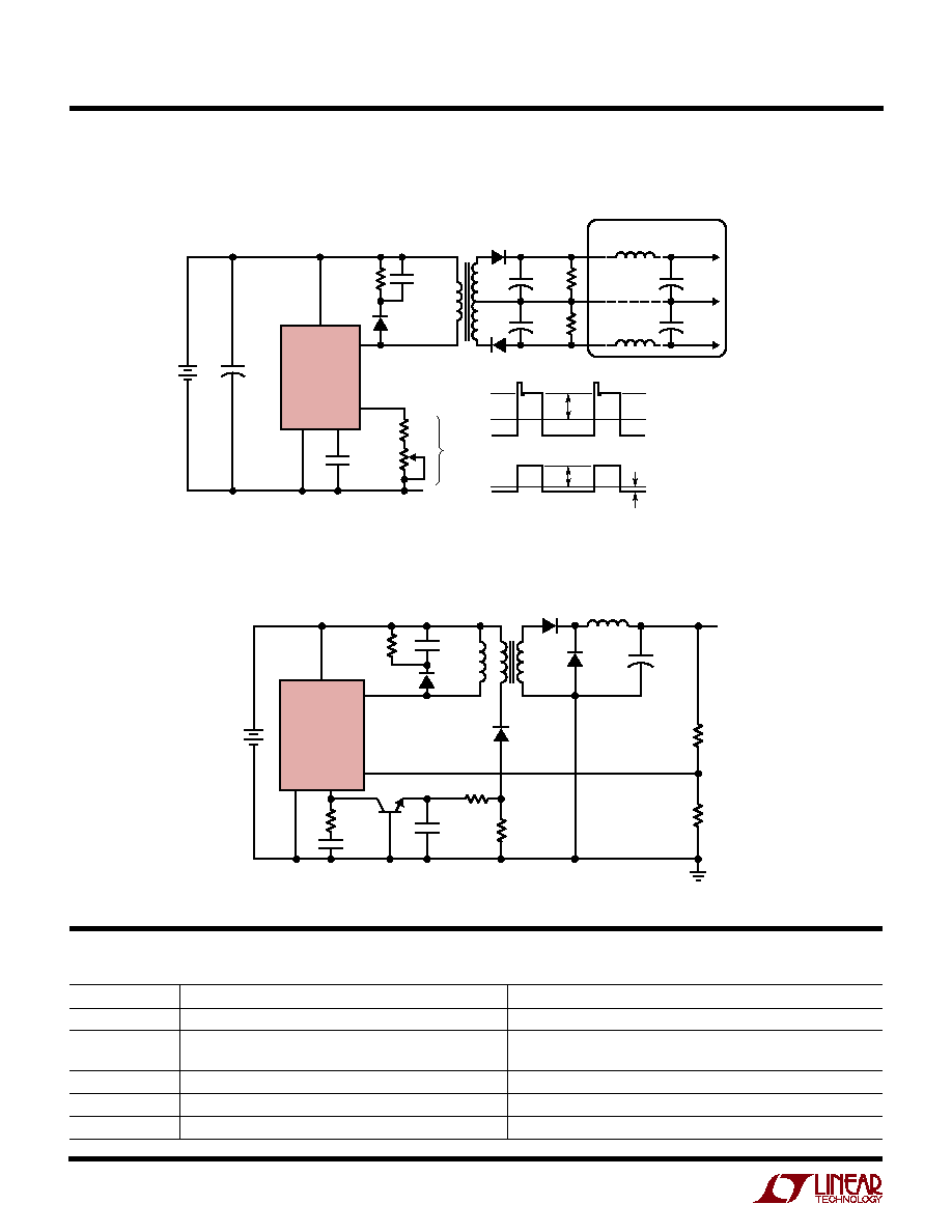
Flyback Converter
1070/71 TA08
*REQUIRED IF INPUT LEADS
2"
a
b
V
SNUB
C2
0.15
µ
F
R3
1.5k
R1
3.74k
R2
1.24k
C4*
100
µ
F
V
IN
20V TO 30V
V
OUT
5V
6A
V
SW
V
C
V
IN
LT1070
GND
FB
C3
0.47
µ
F
C1
2000
µ
F
D2
D1
R4
1 N
∑
∑
+
+
PRIMARY FLYBACK VOLTAGE =
LT1070/LT1071 SWITCH VOLTAGE
AREA "a" = AREA "b" TO MAINTAIN
ZERO DC VOLTS ACROSS PRIMARY
SECONDARY VOLTAGE
AREA "c" = AREA "d" TO MAINTAIN
ZERO DC VOLTS ACROSS SECONDARY
PRIMARY CURRENT
V
OUT
+ V
F
N
0V
V
IN
CLAMP TURN-ON
SPIKE
C4
200
µ
F
L2
10
µ
H
OPTIONAL
FILTER
c
I
d
V
OUT
+ V
F
(N)(V
IN
)
I
PRI
0V
0
LT1070 SWITCH CURRENT
SNUBBER DIODE CURRENT
I
PRI
I
PRI
t =
(I
PRI
)(L
L
)
V
SNUB
SECONDARY CURRENT
I
PRI
N
0
0
N = 1/3
PACKAGE DESCRIPTIO
N
U
OBSOLETE PACKAGE
T Package
5-Lead Plastic TO-220 (Standard)
(Reference LTC DWG # 05-08-1421)
K Package
4-Lead TO-3 Metal Can
(Reference LTC DWG # 05-08-1311)
12
LT1070/LT1071
10701fe
LT/CPI 0202 1.5K REV E ∑ PRINTED IN USA
©
LINEAR TECHNOLOGY CORPORATION 1989
Linear Technology Corporation
1630 McCarthy Blvd., Milpitas, CA 95035-7417
(408) 432-1900
q
FAX: (408) 434-0507
q
www.linear.com
RELATED PARTS
PART NUMBER
DESCRIPTION
COMMENTS
LT1074/LT1076
High Voltage Switching Regulators
40V Input (60V for HV Versions), 100kHz, 5A and 2A
LT1170/LT1171/
100kHz High Efficiency Switching Regulators
40V Input (65V for HV Versions), 5A/2.5A/1.25A Internal Switch
LT1172
LT1370/LT1371
500kHz High Efficiency Switching Regulators
35V, 6A/3A Internal Switch
LT1374/LT1376
100kHz High Efficiency Switching Regulators
25V Input, 4.5A/1.5A Internal Switch
LT1765
1.25MHz, 3A, Step-Down Regulator
25V Input, TSSOP-16E, SO8 Package
Forward Converter
Totally Isolated Converter
1070/71 TA07
R4
1.5k
5k
500
N = 0.875 = 7:8
FOR V
OUT
= 15V
*REQUIRED IF INPUT LEADS
2"
R2
SECONDARY VOLTAGE
0V
V
OUT
t
OFF
t
ON
16V
(N)(V
IN
)
C2
0.01
µ
F
C5*
100
µ
F
V
IN
5V
V
SW
V
C
V
IN
LT1070/LT1071
GND
FB
+
C3
0.47
µ
F
N
D1
1:N
∑
∑
N
+
L1
10
µ
F
L2
10
µ
F
15V
COM
+
C4
500
µ
F
C1
500
µ
F
+
+
C6
200
µ
F
C5
200
µ
F
OPTIONAL
OUTPUT FILTER
+
≠15V
SWITCH VOLTAGE
V
F
(DIODE FORWARD VOLTAGE)
0V
V
IN
+
R3
R6
330
R5
1
Q1
C3
C4
V
SW
L1
70
µ
H
∑
∑
∑
V
IN
C2
D3
C1
2000
µ
F
D1
V
OUT
5V
6A
R4
T1
LT1070
GND
V
C
FB
V
IN
20V TO 30V
D4
I
M
N
D2
1070/71 TA18
R1
3.74k
R2
1.24k
TYPICAL APPLICATIO
N
S
U
(Note that maximum output currents are divided by 2 for the LT1071)