 | –≠–ª–µ–∫—Ç—Ä–æ–Ω–Ω—ã–π –∫–æ–º–ø–æ–Ω–µ–Ω—Ç: LT1072M | –°–∫–∞—á–∞—Ç—å:  PDF PDF  ZIP ZIP |
1
LT1072
1072fc
1.25A High Efficiency
Switching Regulator
Available in MiniDiP, TO-220, and TO-3 Packages
Wide Input Voltage Range 3V to 60V
Low Quiescent Current--6mA
Internal 1.25A Switch
Very Few External Parts Required
Self-Protected Against Overloads
Operates in Nearly All Switching Topologies
Shutdown Mode Draws Only 50µA Supply Current
Flyback-Regulated Mode has Fully Floating Outputs
Can be Externally Synchronized
The LT
Æ
1072 is a monolithic high power switching
regulator. It can be operated in all standard switching
configurations including buck, boost, flyback, forward,
inverting and "Cuk". A high current, high efficiency switch
is included on the die along with all oscillator, control, and
protection circuitry. Integration of all functions allows the
LT1072 to be built in a standard 5-pin TO-3 or TO-220
power package as well as the 8-pin miniDlP. This makes it
extremely easy to use and provides "bust proof" operation
similar to that obtained with 3-pin linear regulators.
The LT1072 operates with supply voltages from 3V to 60V,
and draws only 6mA quiescent current. It can deliver load
power up to 20 watts with no external power devices. By
utilizing current-mode switching techniques, it provides
excellent AC and DC load and line regulation.
The LT1072 has many unique features not found even on
the vastly more difficult to use low power control chips
presently available. It uses an adaptive anti-sat switch
drive to allow very wide ranging load currents with no loss
in efficiency. An externally activated shutdown mode
reduces total supply current to 50µA typical for standby
operation. Totally isolated and regulated outputs can be
generated by using the optional "flyback regulation mode"
built into the LT1072, without the need for optocouplers or
extra transformer windings.
USER NOTE:
This data sheet is only intended to provide specifications, graphs, and a general functional
description of the LT1072. Application circuits are included to show the capability of the LT1072.
A complete design manual (AN-19) should be obtained to assist in developing new designs. This
manual contains a comprehensive discussion of both the LT1070 and the external components used
with it, as well as complete formulas for calculating the values of these components. The manual
can also be used for the LT1072 by factoring in the lower switch current rating.
, LTC and LT are registered trademarks of Linear Technology Corporation.
FEATURES
DESCRIPTIO
U
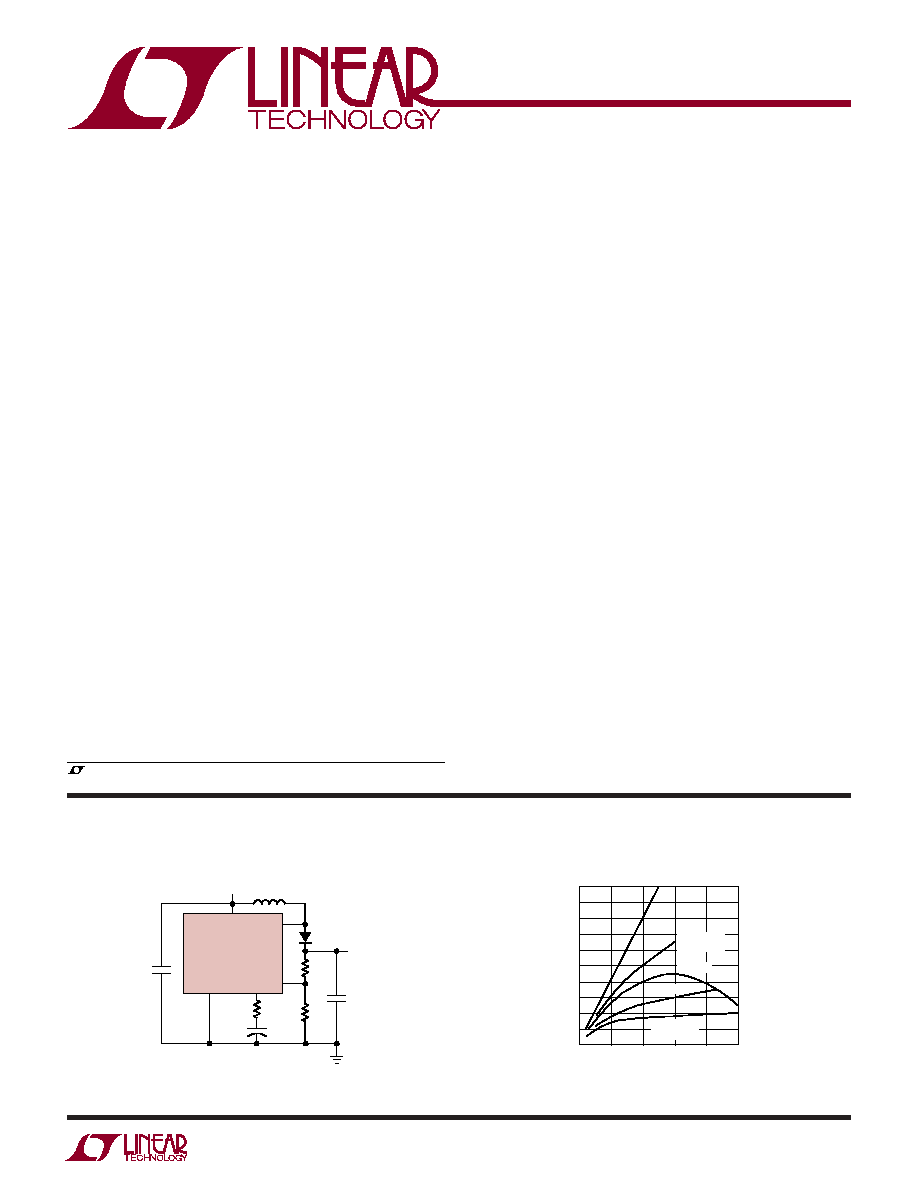
Boost Converter (5V to 12V)
TYPICAL APPLICATIO
U
10.7k
1.24k
LT1072
GND
V
C
V
IN
V
SW
FB
1k
1µF
≠
470µF
12V, 0.25A
*REQUIRED IF INPUT LEADS 2"
**PULSE ENGINEERING 52626
220µH**
5V
+
≠
C3
25µF*
+
≠
LT1072 ∑ TA01
+
Maximum Output Power*
LT1072 ∑ TA02
INPUT VOLTAGE (V)
0
*ROUGH GUIDE ONLY. BUCK MODE P
OUT
= 1A x V
OUT
.
MINIDIP OUTPUT POWER MAY BE LIMITED BY PACKAGE TEMPERATURE
RISE AT HIGH INPUT VOLTAGES OR HIGH DUTY CYCLES
POWER (W)
15
20
25
10
5
0
10
20
30
40
50
BUCK-BOOST
V
O
= 5V
BUCK-BOOST
V
O
= 30V
FLYBACK
ISOLATED
BOOST
Logic Supply 5V at 2.5A
5V Logic to ±15V Op Amp Supply
Offline Converter up to 50W
Battery Upconverter
Power lnverter (+ to ≠) or (≠ to +)
Fully Floating Multiple Outputs
Driver for High Current Supplies
APPLICATIO S
U
2
LT1072
1072fc
Supply Voltage
LT1072HV (See Note 1) ......................................... 60V
LT1072 (See Note 1) ............................................. 40V
Switch Output Voltage
LT1072HV ............................................................. 75V
LT1072 .................................................................. 65V
LT1072S8 .............................................................. 60V
Feedback Pin Voltage (Transient, 1ms) ................. ±15V
Operating Junction Temperature Range
LT1072HVM, LT1072M (OBSOLETE) .... ≠55∞C to 150∞C
LT1072HVC, LT1072C (Oper.)* ............ 0∞C to 100∞C
LT1072HVC, LT1072C (Sh. Ckt.)* ........ 0∞C to 125∞C
LT1072HVI ....................................... ≠40∞C to 125∞C
Storage Temperature Range ............... ≠65∞C to 150∞C
Lead Temperature (Soldering, 10 sec) ............... 300∞C
*Includes LT1072S8
(Note 1)
Consult LTC Marketing for parts specified with wider operating temperature ranges.
Note 1: Minimum switch "on" time for the LT1072 in current limit is
0.7µsec. This limits the maximum input voltage during short-circuit
conditions,
in the buck and inverting modes only,
to 40V. Normal
(unshorted) conditions are not affected. If the LT1072 is being operated in
the buck or inverting mode at high input voltages and short-circuit
conditions are expected, a resistor must be placed in series with the
inductor, as follows:
The value of the resistor is given by:
R =
≠ R
L
(t) (f) (V
IN
) ≠ V
f
I
(LIMIT)
t = Minimum "on" time of LT1072 in current limit, 0.7µs
f = Operating frequency (40kHz)
V
f
= Forward voltage of external catch diode at I
(LIMIT)
I
(LIMIT)
= Current limit of LT1072 (2A)
R
L
= Internal series resistance of inductor
OBSOLETE PACKAGE
OBSOLETE PACKAGE
Consider the S8 or N8 Packages for Alternate Source
T PACKAGE
5-LEAD TO-220
T
JMAX
= 100
∞
C/W,
JC
= 8
∞
C/W,
JA
= 50
∞
C/W
V
IN
V
C
GND
FB
V
SW
FRONT VIEW
5
4
3
2
1
N PACKAGE
8-LEAD PDIP
T
JMAX
= 100
∞
C,
JA
= 130
∞
C/W
J PACKAGE
8-LEAD CERAMIC DIP
T
JMAX
= 150
∞
C,
JA
= 100
∞
C/W
1
2
3
4
8
7
6
5
TOP VIEW
GND
V
C
FB
NC
E2
V
SW
E1
V
IN
1
2
3
4
5
6
7
8
SW PACKAGE
16-LEAD PLASTIC SO WIDE
T
JMAX
= 100
∞
C,
JC
= 130
∞
C/W
16
15
14
13
12
11
10
9
NC
NC
GND
V
C
FB
NC
NC
NC
NC
NC
E2
V
SW
E1
V
IN
NC
NC
TOP VIEW
BOTTOM VIEW
K PACKAGE
4-LEAD TO-3 METAL CAN
T
JMAX
= 150
∞
C,
JC
= 8
∞
C/W,
JA
= 35
∞
C/W
T
JMAX
= 100
∞
C*,
JC
= 8
∞
C/W,
JA
= 35
∞
C/W
CASE IS
GND
V
C
1
4
2
3
FB
V
SW
V
IN
LT1072HVMK
LT1072MK
LT1072HVCK
LT1072CK
ORDER PART
NUMBER
ORDER PART
NUMBER
ORDER PART
NUMBER
ORDER PART
NUMBER
LT1072CT
LT1072HVCT
LT1072HVIT
LT1072CN8
LT1072CS8
LT1072MJ8
LT1072CJ8
LT1072CSW
LT1072 ∑ POI01
1
2
3
4
8
7
6
5
TOP VIEW
E2
V
SW
E1
V
IN
GND
V
C
FB
NC
S8 PACKAGE
8-LEAD PLASTIC SO
T
JMAX
= 100
∞
C,
JA
= 130
∞
C/W
S8 PART
MARKING
1072
ABSOLUTE AXI U RATI GS
W
W
W
U
PACKAGE/ORDER I FOR ATIO
U
U
W
3
LT1072
1072fc
SYMBOL
PARAMETER
CONDITlONS
MIN
TYP
MAX
UNITS
V
REF
Reference Voltage
Measured at Feedback Pin
1.224
1.244
1.264
V
V
C
= 0.8V
1.214
1.244
1.274
V
I
B
Feedback Input Current
V
FB
= V
REF
350
750
nA
1100
nA
gm
Error Amplifier
I
C
= ±25µA
3000
4400
6000
µmho
Transconductance
2400
7000
µmho
Error Amplifier Source or
V
C
= 1.5V
150
200
350
µA
Sink Current
120
400
µA
Error Amplifier Clamp
Hi Clamp, V
FB
= 1V
1.8
2.3
V
Voltage
Lo Clamp, V
FB
= 1.5V
0.25
0.38
0.52
V
Reference Voltage Line
3V V
IN
V
MAX
0.03
%/V
Regulation
V
C
= 0.8V
%/V
A
V
Error Amplifier Voltage Gain
0.9V V
C
1.4V
500
800
V/V
Minimum Input Voltage
2.6
3.0
V
I
Q
Supply Current
3V V
IN
V
MAX
, V
C
= 0.6V
6
9
mA
Control Pin Threshold
Duty Cycle = 0
0.8
0.9
1.08
V
0.6
1.25
V
Normal/Flyback Threshold on Feedback Pin
0.4
0.45
0.54
V
V
FB
Flyback Reference Voltage
l
FB
= 50µA
15
16.3
17.6
V
14
18
V
Change in Flyback Reference Voltage
0.05 I
FB
1mA
4.5
6.8
8.5
V
Flyback Reference Voltage
l
FB
= 50µA
0.01
0.03
%/V
Line Regulation
3V V
IN
V
MAX
(Note 4)
%/V
Flyback Amplifier Transconductance (gm)
I
C
= ±10µA
150
300
650
µmho
Flyback Amplifier Source
V
C
= 0.6V Source
15
32
70
µA
and Sink Current
I
FB
= 50µA Sink
25
40
70
µA
BV
Output Switch Breakdown
3V V
IN
V
MAX
LT1072
65
90
V
Voltage
I
SW
= 1.5mA
LT1072HV
75
90
V
LT1072S8
60
80
V
V
SAT
Output Switch ON Resistance (Note 2)
I
SW
= 1.25A
0.6
1
Control Voltage to Switch Current Transconductance
2
A/V
I
LIM
Switch Current Limit
Duty Cycle = 50%
T
J
25∞C
1.25
3
A
Duty Cycle = 50%
T
J
< 25∞C
1.25
3.5
A
Duty Cycle = 80% (Note 3)
1
2.5
A
I
IN
Supply Current Increase
25
35
mA/A
I
SW
During Switch ON Time
f
Switching Frequency
35
40
45
kHz
33
47
kHz
DC (max)
Maximum Switch Duty Cycle
90
92
97
%
Flyback Sense Delay Time
1.5
µs
Shutdown Mode
3V V
IN
V
MAX
100
250
µA
Supply Current
V
C
= 0.05V
Shutdown Mode
3V V
IN
V
MAX
100
150
250
mV
Threshold Voltage
50
300
mV
The
denotes specifications which apply over the full operating
temperature range. Unless otherwise specified, V
IN
= 15V, V
C
= 0.5V, V
FB
= V
REF
, output pin open.
Note 1: Absolute Maximum Ratings are those values beyond which the life
of a device may be impaired.
Note 2: Measured with V
C
in hi clamp, V
FB
= 0.8V.
Note 3: For duty cycles (DC) between 50% and 80%, minimum
guaranteed switch current is given by I
LIM
= 0.833 (2 ≠ DC).
Note 4: V
MAX
= 55V for LT1072HV to avoid switch breakdown.
ELECTRICAL CHARACTERISTICS
4
LT1072
1072fc
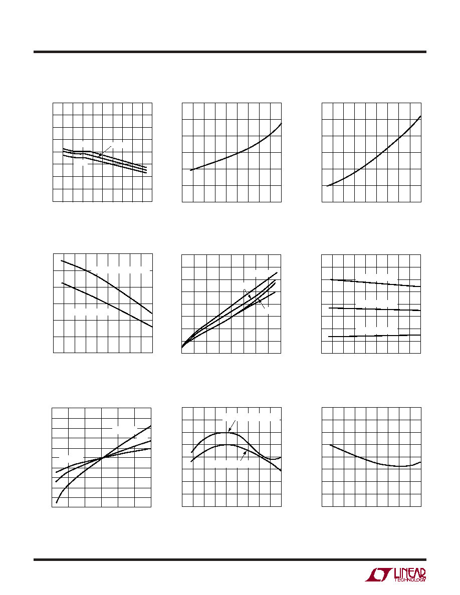
Switch Current Limit vs Duty Cycle
Maximum Duty Cycle
Flyback Blanking Time
DUTY CYCLE (%)
0
SWITCH CURRENT (A)
4
3
2
1
0
80
LT1072 ∑ TPC01
20
40
60
100
70
10
30
50
90
≠55∞C
125∞C
25∞C
JUNCTION TEMPERATURE (∞C)
≠75
90
DUTY CYCLE (%)
91
93
94
95
≠25
25
50
150
LT1072 ∑ TPC02
92
≠50
0
75 100 125
96
JUNCTION TEMPERATURE (∞C)
≠75
1.0
TIME (
µ
s)
1.2
1.6
1.8
2.0
≠25
25
50
150
LT1072 ∑ TPC03
1.4
≠50
0
75 100 125
2.2
Minimum Input Voltage
Switch Saturation Voltage
Isolated Mode Flyback Reference
Voltage
TEMPERATURE (∞C)
≠75
2.3
MINIMUM INPUT VOLTAGE (V) 2.4
2.6
2.7
2.8
≠25
25
50
150
LT1072 ∑ TPC04
2.5
≠50
0
75 100 125
2.9
SWITCH CURRENT = 1.25A
SWITCH CURRENT = 0A
SWITCH CURRENT (A)
0
SWITCH SATURATION VOLTAGE (V)
0.8
1.2
2
LT1072 ∑ TPC05
0.4
0
0.5
1
1.5
0.25
0.75
1.25
1.75
1.6
0.6
1.0
0.2
1.4
150∞C
100∞C
≠55∞C
25∞C
TEMPERATURE (C∞)
≠75
FLYBACK VOLTAGE (V)
19
20
21
125
LT1072 ∑ TPC06
18
17
15
≠25
25
75
≠50
150
0
50
100
16
23
22
R
FEEDBACK
= 500
R
FEEDBACK
= 1k
R
FEEDBACK
= 10k
Line Regulation
Reference Voltage and Switching
Frequency vs Temperature
Feedback Bias Current vs
Temperature
INPUT VOLTAGE (V)
0
≠ 5
REFERENCE VOLTAGE CHANGE (mV)
≠ 3
≠1
1
10
20
30
40
LT1072 ∑ TPC07
50
3
5
≠ 4
≠ 2
0
2
4
60
T
J
= 150∞C
T
J
= ≠ 55∞C
T
J
= 25∞
C
TEMPERATURE (∞C)
≠75
REFERENCE VOLTAGE (V)
FREQUENCY (kHz)
1.242
1.244
1.246
125
LT1072 ∑ TPC08
1.240
1.238
1.234
≠25
25
75
≠50
150
0
50
100
1.236
1.250
1.248
38
39
40
37
36
34
35
42
41
REFERENCE VOLTAGE
SWITCHING FREQUENCY
TEMPERATURE (∞C)
≠75
FEEDBACK BIAS CURRENT (nA)
400
500
600
125
LT1072 ∑ TPC09
300
200
0
≠25
25
75
≠50
150
0
50
100
100
800
700
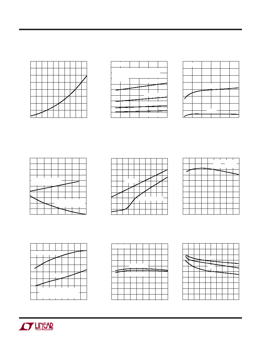
TYPICAL PERFOR A CE CHARACTERISTICS
U
W
5
LT1072
1072fc
Driver Current* vs Switch Current
Supply Current vs Input Voltage*
Supply Current vs Supply Voltage
(Shutdown Mode)
Normal/Flyback Mode Threshold
on Feedback Pin
Shutdown Mode Supply Current
Error Amplifier Transconductance
Shutdown Thresholds
Idle Supply Current vs
Temperature
Feedback Pin Clamp Voltage
SWITCH CURRENT (A)
0
*AVERAGE LT1072 POWER SUPPLY CURRENT IS
FOUND BY MULTIPLYING DRIVER CURRENT BY
DUTY CYCLE, THEN ADDING QUIESCENT CURRENT
DRIVER CURRENT (mA)
80
70
60
50
40
30
20
10
0
1.6
LT1072 ∑ TPC10
0.4
0.8
1.2
2
1.4
0.2
0.6
1
1.8
*UNDER VERY LOW OUTPUT CURRENT CONDITIONS,
DUTY CYCLE FOR MOST CIRCUITS WILL APPROACH
10% OR LESS
INPUT VOLTAGE (V)
0
5
SUPPLY CURRENT (mA)
7
9
11
10
20
30
40
LT1072 ∑ TPC11
50
13
15
6
8
10
12
14
60
T
J
= 25∞C
NOTE THAT THIS CURRENT DOES NOT
INCLUDE DRIVER CURRENT, WHICH IS
A FUNCTION OF LOAD CURRENT AND
DUTY CYCLE.
90% DUTY CYCLE
50% DUTY CYCLE
10% DUTY CYCLE
0% DUTY CYCLE
SUPPLY VOLTAGE (V)
0
SUPPLY CURRENT (
µ
A)
60
80
100
30
50
LT1072 ∑ TPC12
40
20
0
10
20
40
120
140
160
60
T
J
= 25∞C
V
C
= 50mV
V
C
= 0V
TEMPERATURE (∞C)
≠50
400
FEEDBACK PIN VOLTAGE (mV)
FEEDBACK PIN CURRENT (
µ
A)
410
430
440
450
500
470
0
50
75
LT1072 ∑ TPC13
420
480
490
460
≠4
≠6
≠10
≠12
≠14
≠24
≠18
≠8
≠20
≠22
≠16
≠25
25
100 125
150
FEEDBACK PIN VOLTAGE
(AT THRESHOLD)
FEEDBACK PIN CURRENT
(AT THRESHOLD)
V
C
PIN VOLTAGE (mV)
0
SUPPLY CURRENT (
µ
A)
120
160
200
80
LT1072 ∑ TPC14
80
40
100
140
180
60
20
0
20
10
40
30
60 70
90
50
100
T
J
= 150∞C
≠ 55∞C T
J
125∞C
TEMPERATURE (C∞)
≠75
0
TRANSCONDUCTANCE (
µ
mho)
500
1500
2000
2500
5000
3500
≠25
25
50
150
LT1072 ∑ TPC15
1000
4000
4500
3000
≠50
0
75 100 125
G
m
=
I
V
(V
C
PIN)
(FB PIN)
TEMPERATURE (∞C)
≠75
V
C
PIN VOLTAGE (mV)
V
C
PIN VOLTAGE (
µ
A)
200
250
300
125
LT1072 ∑ TPC16
150
100
0
≠25
25
75
≠50
150
0
50
100
50
400
350
≠200
≠250
≠300
≠150
≠100
0
≠50
≠400
≠350
CURRENT (OUT OF V
C
PIN)
VOLTAGE
V
C
VOLTAGE IS REDUCED UNTIL
REGULATOR CURRENT DROPS
BELOW 300µA
TEMPERATURE (∞C)
≠75
1
IDLE SUPPLY CURRENT (mA)
2
4
5
6
11
8
≠25
25
50
150
LT1072 ∑ TPC17
3
9
10
7
≠50
0
75 100 125
V
C
= 0.6V
V
SUPPLY
= 60V
V
SUPPLY
= 3V
FEEDBACK CURRENT (mA)
0
FEEDBACK VOLTAGE (mV)
300
400
500
0.8
LT1072 ∑ TPC18
200
100
250
350
450
150
50
0
0.2
0.1
0.4
0.3
0.6 0.7
0.9
0.5
1
≠55∞C
25∞C
150∞C
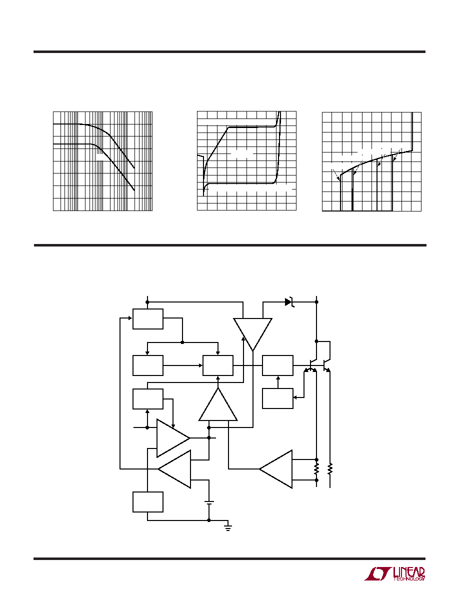
TYPICAL PERFOR A CE CHARACTERISTICS
U
W
6
LT1072
1072fc
Transconductance of Error
Amplifier
V
C
Pin Characteristics
Switch "Off" Characteristics
FREQUENCY (Hz)
1000
TRANSCONDUCTANCE (
µ
mho)
PHASE (
∞
)
3000
4000
6000
7000
1k
100k
1M
10M
LT1072 ∑ TPC19
≠1000
10k
5000
2000
0
150
90
60
0
≠30
210
30
120
180
G
m
V
C
PIN VOLTAGE (V)
0
≠400
V
C
PIN CURRENT (
µ
A)
≠300
≠200
≠100
300
100
0.5
1.0
200
0
1.5
2.0
2.5
LT1072 ∑ TPC20
V
FB
= 1.5V (CURRENT INTO V
C
PIN)
V
FB
= 0.8V (CURRENT OUT OF V
C
PIN)
T
J
= 25∞C
SWITCH VOLTAGE (V)
0
SWITCH CURRENT (
µ
A)
600
800
1000
80
LT1072 ∑ TPC21
400
200
500
700
900
300
100
0
20
10
40
30
60 70
90
50
100
V
SUPPLY
= 55V
V
SUPPLY
= 40V
V
SUPPLY
= 15V
V
SUPPLY
= 3V
≠
+
2.3V
REG
40kHz
OSC
FB
V
C
SHUTDOWN
CIRCUIT
0.15V
0.16
GAIN
6
GND
MODE
SELECT
LOGIC
COMP
V
IN
FLYBACK
ERROR
AMP
DRIVER
ANTI-
SAT
SWITCH
OUT
16V
≠
+
0.16
E1*
* ALWAYS CONNECT E1 TO GROUND PIN ON MINIDIP AND SURFACE MOUNT
PACKAGES. EMITTERS TIED TO GROUND ON TO-3 AND TO-220 PACKAGES
E2
1.24V
REF
ERROR
AMP
CURRENT
AMP
LT1072 ∑ BD01
TYPICAL PERFOR A CE CHARACTERISTICS
U
W
BLOCK DIAGRA
W

7
LT1072
1072fc
The LT1072 is a current mode switcher. This means that
switch duty cycle is directly controlled by switch current
rather than by output voltage. Referring to the block
diagram, the switch is turned "on" at the start of each
oscillator cycle. It is turned "off" when switch current
reaches a predetermined level. Control of output voltage is
obtained by using the output of a voltage sensing error
amplifier to set current trip level. This technique has
several advantages. First, it has immediate response to
input voltage variations, unlike ordinary switchers which
have notoriously poor line transient response. Second, it
reduces the 90 phase shift at midfrequencies in the energy
storage inductor. This greatly simplifies closed loop fre-
quency compensation under widely varying input voltage
or output load conditions. Finally, it allows simple pulse-
by-pulse current limiting to provide maximum switch
protection under output overload or short conditions. A
low-dropout internal regulator provides a 2.3V supply for
all internal circuitry on the LT1072. This low-dropout
design allows input voltage to vary from 3V to 60V with
virtually no change in device performance. A 40kHz
oscillator is the basic clock for all internal timing. It turns
"on" the output switch via the logic and driver circuitry.
Special adaptive antisat circuitry detects onset of
saturation in the power switch and adjusts driver current
instantaneously to limit switch saturation. This minimizes
driver dissipation and provides very rapid turn-off of
the switch.
A 1.2V bandgap reference biases the positive input of the
error amplifier. The negative input is brought out for
output voltage sensing. This feedback pin has a second
function; when pulled low with an external resistor, it
programs the LT1072 to disconnect the main error
amplifier output and connects the output of the flyback
amplifier to the comparator input. The LT1072 will then
regulate the value of the flyback pulse with respect to the
supply voltage. This flyback pulse is directly proportional
to output voltage in the traditional transformer coupled
flyback topology regulator. By regulating the amplitude of
the flyback pulse, the output voltage can be regulated with
no direct connection between input and output. The output
is fully floating up to the breakdown voltage of the
transformer windings. Multiple floating outputs are easily
obtained with additional windings. A special delay network
inside the LT1072 ignores the leakage inductance spike at
the leading edge of the flyback pulse to improve output
regulation.
The error signal developed at the comparator input is
brought out externally. This pin (V
C
) has four different
functions. It is used for frequency compensation, current
limit adjustment, soft starting, and total regulator
shutdown. During normal regulator operation this pin sits
at a voltage between 0.9V (low output current) and 2.0V
(high output current). The error amplifiers are current
output (gm) types, so this voltage can be externally
clamped for adjusting current limit. Likewise, a capacitor
coupled external clamp will provide soft start. Switch duty
cycle goes to zero if the V
C
pin is pulled to ground through
a diode, placing the LT1072 in an idle mode. Pulling the V
C
pin below 0.15V causes total regulator shutdown, with
only 50µA supply current for shutdown circuitry biasing.
See AN-19 for full application details.
Extra Pins on the MiniDIP and Surface Mount Packages
The 8 and 16-pin versions of the LT1072 have the emitters
of the power transistor brought out separately from the
ground pin. This eliminates errors due to ground pin
voltage drops and allows the user to reduce switch current
limit 2:1 by leaving the second emitter (E2) disconnected.
The first emitter (E1) should always be connected to the
ground pin. Note that switch "on" resistance doubles
when E2 is left open, so efficiency will suffer somewhat
when switch currents exceed 100mA. Also, note that chip
dissipation will actually
increase with E2 open during
normal load operation, even though dissipation in current
limit mode will
decrease. See "Thermal Considerations."
Thermal Considerations When Using Small Packages
The low supply current and high switch efficiency of the
LT1072 allow it to be used without a heat sink in most
applications when the TO-220 or TO-3 package is selected.
These packages are rated at 50∞C/W and 35∞C/W
respectively. The small packages, however, are rated at
greater than 100∞C/W. Care should be taken with these
packages to ensure that the worse case input voltage and
load current conditions do not cause excessive die
temperatures. The following formulas can be used as a
LT1072 OPERATIO
U

8
LT1072
1072fc
rough guide to calculate LT1072 power dissipation. For
more details, the reader is referred to Application Note 19
(AN19), "Efficiency Calculations" section.
Average supply current (including driver current) is:
I
IN
6mA + I
SW
(0.004 + DC/40)
I
SW
= switch current
DC = switch duty cycle
Switch power dissipation is given by:
P
SW
= (I
SW
)
2
∑ R
SW
∑ DC
R
SW
= LT1072 switch "on" resistance (1 maximum)
Total power dissipation is the sum of supply current times
input voltage plus switch power:
P
TOT
= (l
lN
)(V
IN
) + P
SW
In a typical example, using a boost converter to generate
12V @ 0.12A from a 5V input, duty cycle is approximately
60%, and switch current is about 0.65A, yielding:
l
lN
= 6mA + 0.65(0.004 + DC/40) = 18mA
P
SW
= (0.65)
2
∑ 1 ∑ (0.6) = 0.25W
P
TOT
= (5V)(0.018A) + 0.25 = 0.34W
Temperature rise in a plastic miniDIP would be 130∞C/W
times 0.34W, or approximately 44∞C. The maximum
ambient temperature would be limited to 100∞C
(commercial temperature limit) minus 44∞C, or 56∞C.
In most applications, full load current is used to calculate
die temperature. However, if overload conditions must
also be accounted for, four approaches are possible. First,
if loss of regulated output is acceptable under overload
conditions, the internal
thermal limit of the LT1072 will
protect the die in most applications by shutting off switch
current.
Thermal limit is not a tested parameter, however,
and should be considered only for non-critical applications
with temporary overloads. A second approach is to use the
larger TO-220 (T) or TO-3 (K) package which, even without
a heat sink, may limit die temperatures to safe levels under
overload conditions. In critical situations, heat sinking
of these packages is required; especially if overload
conditions must be tolerated for extended periods of time.
The third approach for lower current applications is to
leave the second switch emitter open. This increases
switch "on" resistance by 2:1, but reduces switch current
limit by 2:1 also, resulting in a net 2:1 reduction in I
2
R
switch dissipation under current limit conditions.
The fourth approach is to clamp the V
C
pin to a voltage less
than its internal clamp level of 2V. The LT1072 switch
current limit is zero at approximately 1V on the V
C
pin and
2A at 2V on the V
C
pin. Peak switch current can be
externally clamped between these two levels with a diode.
See AN-19 for details.
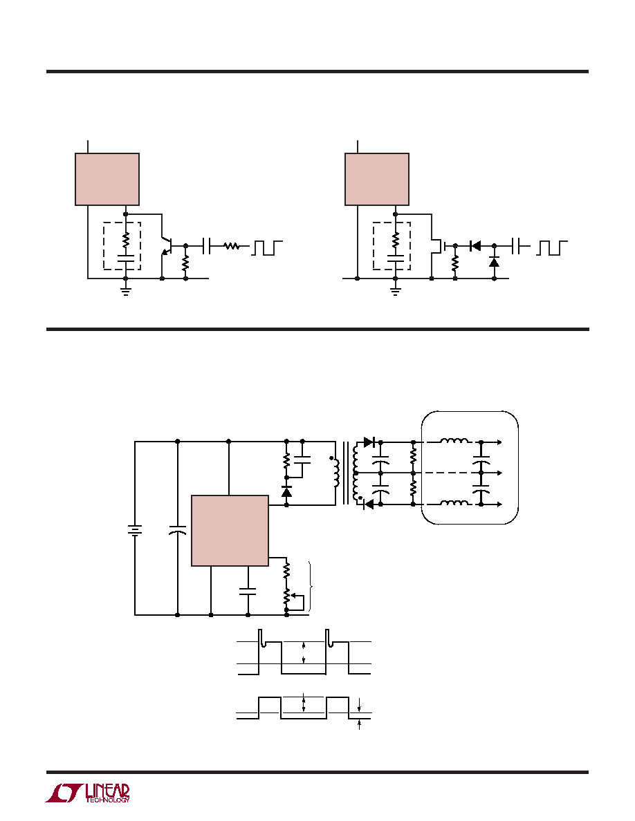
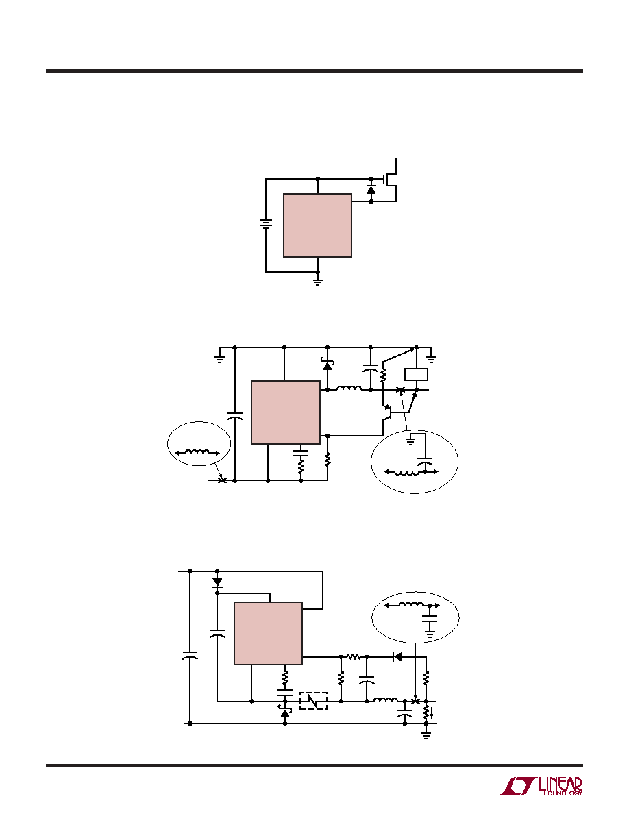
LT1072 Synchronizing
The LT1072 can be externally synchronized in the frequency
range of 48kHz to 70kHz. This is accomplished as shown
in the accompanying figures. Synchronizing occurs when
the V
C
pin is pulled to ground with an external transistor.
To avoid disturbing the DC characteristics of the internal
error amplifier, the width of the synchronizing pulse
should be under 1µs. C2 sets the pulse width at 0.35µs.
The effect of a synchronizing pulse on the LT1072
amplifier offset can be calculated from:
KT
= 26mV at 25∞C
q
t
S
= pulse width
f
S
= pulse frequency
I
C
= LT1072 V
C
source current ( 200µA)
V
C
= LT1072 operating V
C
voltage (1V to 2V)
R3 = resistor used to set mid-frequency "zero" in LT1072
frequency compensation network.
With t
S
= 0.35µs, f
S
= 50kHz, V
C
= 1.5V, and R3 = 2K,
offset voltage shift is 2.2mV. This is not particularly
bothersome, but note that high offsets could result
if R3 were reduced to a much lower value. Also, the
synchronizing transistor must sink higher currents with
low values of R3, so larger drives may have to be used. The
transistor must be capable of pulling the V
C
pin to within
200mV of ground to ensure synchronizing.
LT1072 OPERATIO
U
V
OS
=
(t
S
)(f
S
) I
C
+
I
C
KT
q
(
(
(
V
C
R3
(
9
LT1072
1072fc
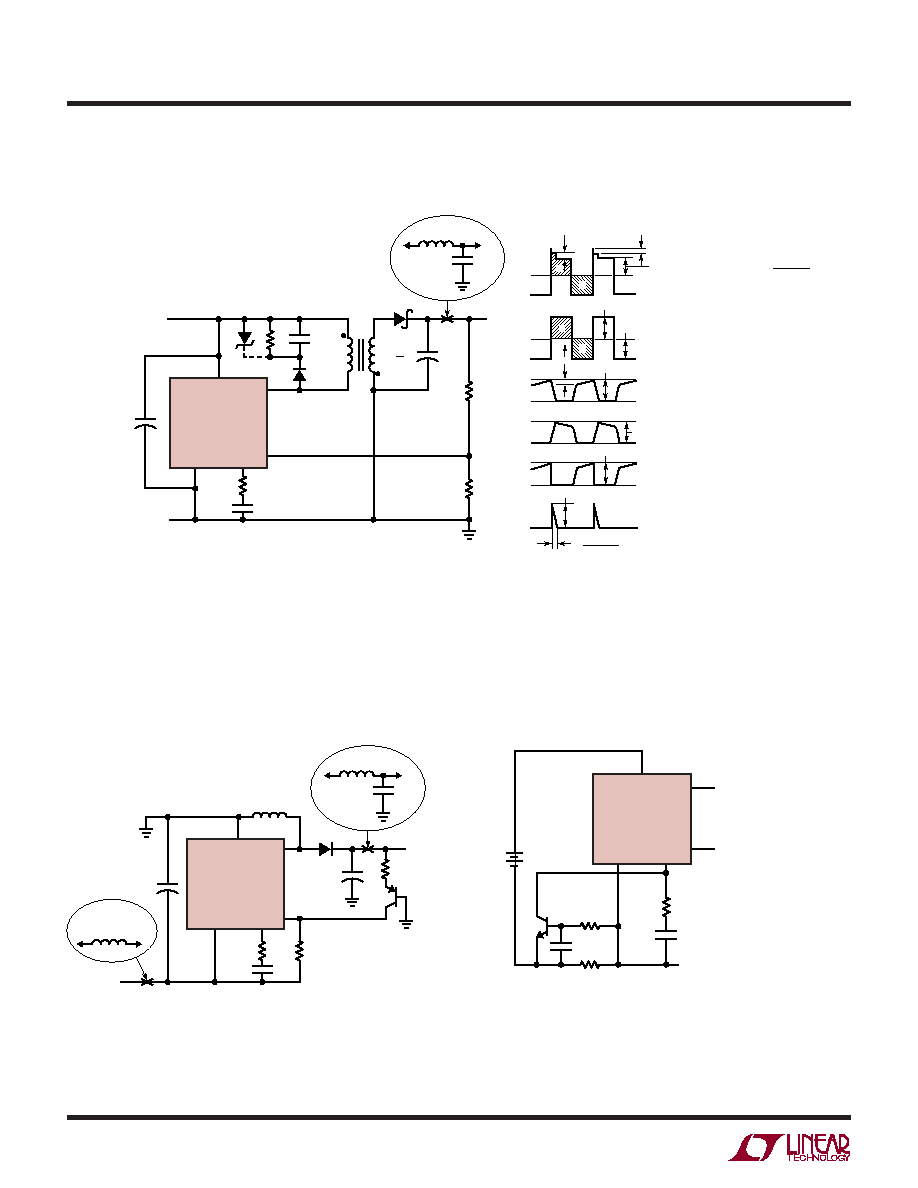
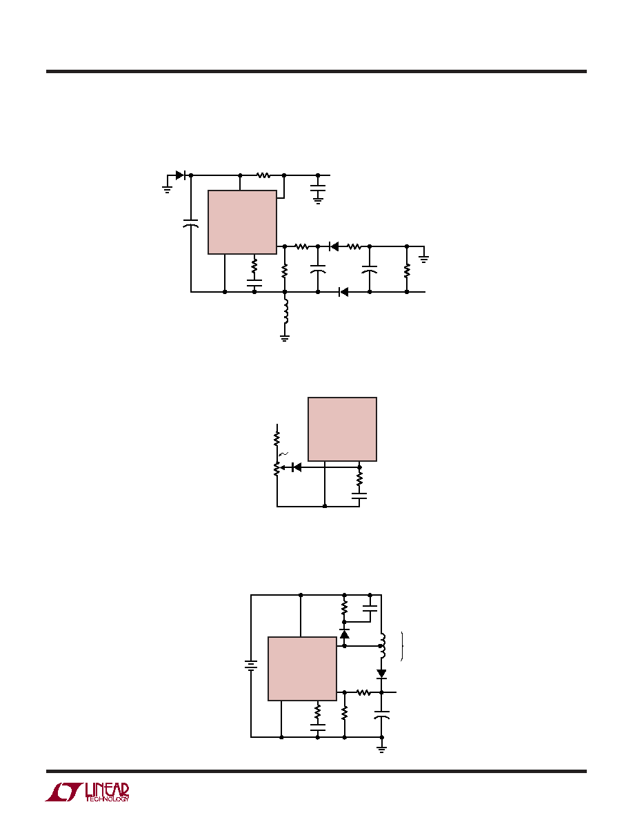
Totally Isolated Converter
Synchronizing with Bipolar Transistor
Synchronizing with MOS Transistor
FROM 5V
LOGIC
R1
3k
R2
2.2k
C2
68pF
V
IN
V
C
GND
LT1072
2N2369
R3
C1
LT1072 ∑ OP01
FROM 5V
LOGIC
*SILICONIX OR EQUIVALENT
R2
2.2k
D2
1N4158
C2
200pF
D1
1N4158
V
IN
V
C
GND
LT1072
R3
C1
VN2222*
LT1072 ∑ OP02
LT1072 OPERATIO
U
C5
25µF*
R4
2.7k
C3
0.47µF
C2
0.01µF
1:N
D1
COM
15V
L1
10µH
OPTIONAL
OUTPUT FILTER
N
N
V
IN
5V
500
R2
*REQUIRED IF INPUT LEADS 2"
N = 0.875 = 7:8
FOR V
OUT
= 15V
5k
C1
200µF
C5
200µF
C6
200µF
C4
200µF
≠15V
L2
10µH
V
IN
V
SW
FB
V
C
GND
LT1072
SWITCH VOLTAGE
V
OUT
+ V
f
(V
f
= DIODE FORWARD VOLTAGE)
t
OFF
t
ON
V
IN
0
0V
SECONDARY VOLTAGE
N ∑ V
IN
16V
LT1072 ∑ TA03
+
+
+
+
+
TYPICAL APPLICATIO S
U
10
LT1072
1072fc
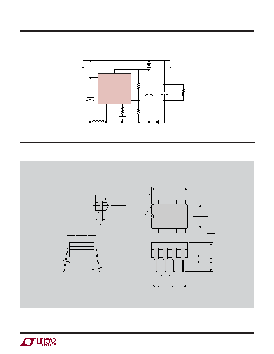
Flyback Converter
Negative to Positive Buck-Boost Converter
External Current Limit
R1
1k
V
IN
NOTE THAT THE LT1072 GND PIN
IS NO LONGER COMMON TO V
IN
(≠)
LT1072 ∑ TA06
C1
1000pF
C2
R
S
R2
+
≠
V
IN
V
SW
FB
V
C
GND
LT1072
Q1
C3
0.47µF
V
OUT
5V
1.5A
D2
D1
OPTIONAL
FILTER
1
1
3
N*
N* =
C2
0.15µF
C4
25µF*
V
IN
20 TO 30V
R3
1.5k
REQUIRED IF INPUT LEADS 2"
OPTIONAL TO REPLACE R4 AND C3
*
**
C1
500µF
R4
1k
**
R1
3.74k
R2
1.24k
V
IN
V
SW
FB
V
C
GND
LT1072
L2
10µH
C4
200µF
V
SNUB
V
OUT
+ V
f
I
PRI
I
PRI
I
PRI
(I
PRI
) (L
L
)
V
SNUB
I
PRI
N
I
V
IN
0V
0V
0
0
0
0
CLAMP TURN-ON
SPIKE
PRIMARY FLYBACK VOLTAGE =
LT1072 SWITCH VOLTAGE
AREA "a" = AREA "b" TO MAINTAIN
ZERO DC VOLTS ACROSS PRIMARY
SECONDARY VOLTAGE
AREA "c" = AREA "d" TO MAINTAIN
ZERO DC VOLTS ACROSS SECONDARY
PRIMARY CURRENT
SECONDARY CURRENT
LT1070 SWITCH CURRENT
SNUBBER DIODE CURRENT
V
OUT
+ V
f
N
N ∑ V
IN
t =
a
b
c
d
LT1072 ∑ TA04
+
+
V
IN
V
SW
FB
V
C
GND
LT1072
C2
1000µF
C1
0.22µF
C4
25µF*
R2
1.24k
R3
2.2k
R1
11.3k
V
OUT
12V, 0.5A
V
IN
≠12V
D1
L1**
220µH
Q1
*
**
REQUIRED IF INPUT LEADS 2"
PULSE ENGINEERING 52626
OPTIONAL
INPUT
FILTER
L3
OPTIONAL
OUTPUT
FILTER
L2
C3
LT1072 ∑ TA05
+
+
TYPICAL APPLICATIO S
U
11
LT1072
1072fc
Positive to Negative Buck-Boost Converter
External Current Limit
LT1072 ∑ TA08
D1
R1
500
R2
2V
V
X
V
C
GND
LT1072
Voltage Boosted Boost Converter
LT1072 ∑ TA09
D2
D1
TOTAL INDUCTANCE = 8mH
INTERLEAVE PRIMARY AND
SECONDARY FOR LOW LEAKAGE
INDUCTANCE
1
L1
N = 5
+
C2
0.047µF
R3
10k
V
IN
15V
C1
200µF
R4
1.5k
1/2W
C3
0.68
R1
98k
V
OUT
100V AT 75mA
R2
1.24k
V
IN
V
SW
FB
V
C
GND
LT1072
+
C
C5
100µF*
V
IN
10 TO 30V
*REQUIRED IF INPUT LEADS 2"
**PULSE ENGINEERING 92113
TO AVOID START-UP PROBLEMS
FOR INPUT VOLTAGES BELOW 10V,
CONNECT ANODE OF D3 TO V
IN
,
AND REMOVE R5. C1 MAY BE
REDUCED FOR LOWER OUTPUT
CURRENTS. C1 (500µF)(I
OUT
).
FOR 5V OUTPUTS, REDUCE R3
TO 1.5k, INCREASE C2 TO 0.3µF,
AND REDUCE R6 TO 100
LT1072 ∑ TA07
R4
47
D1
D2
1N914
C1
1000µF
C
C3
2µF
R5
470, 1W
C
C2
0.1µF
D3
1N4001
C4
5µF
R6
470
R2
1.24k
L1**
200µH
R3
5k
V
OUT
≠12V AT 2A
R1
10.7k
V
IN
V
SW
FB
V
C
GND
LT1072
+
+
+
TYPICAL APPLICATIO S
U
12
LT1072
1072fc
Negative Buck Converter
LT1072 ∑ TA11
R3
C3
25µF*
V
IN
≠20V
R2
1.24k
Q1
2N3906
R1
4.64k
C2
500µF
D1
L1**
220µH
C1
V
IN
V
SW
FB
V
C
GND
LT1072
LOAD
≠5.2V AT 1A
OPTIONAL
OUTPUT
FILTER
L2
4µH
C4
200µF
OPTIONAL
INPUT
FILTER
L3
REQUIRED IF INPUT LEADS 2"
PULSE ENGINEERING 52626
*
**
+
+
+
Positive Buck Converter
Driving High Voltage FET
(for Offline Applications, See AN-25)
LT1072 ∑ TA10
+
10 TO 20V
V
IN
V
SW
GND
LT1072
D1
G
D
Q1
LT1072 ∑ TA12
C1
1µF
R3
470
OPTIONAL
OUTPUT
FILTER
REQUIRED IF INPUT LEADS 2"
PULSE ENGINEERING 52626
*
**
D1
r
D2
L2
4µH
1N914
V
IN
V
SW
FB
V
C
GND
LT1072
R2
1.24k
R4
10
100mA
MINIMUM
5V, 1A
C3
2.2µF
C2
1µF
D3
V
IN
R1
3.74k
L1**
220µH
C4
500µF
C5*
25µF
C5
200µF
+
+
+
+
TYPICAL APPLICATIO S
U
13
LT1072
1072fc
J8 0801
.014 ≠ .026
(0.360 ≠ 0.660)
.200
(5.080)
MAX
.015 ≠ .060
(0.381 ≠ 1.524)
.125
3.175
MIN
.100
(2.54)
BSC
.300 BSC
(7.62 BSC)
.008 ≠ .018
(0.203 ≠ 0.457)
0∞ ≠ 15∞
.005
(0.127)
MIN
.405
(10.287)
MAX
.220 ≠ .310
(5.588 ≠ 7.874)
1
2
3
4
8
7
6
5
.025
(0.635)
RAD TYP
.045 ≠ .068
(1.143 ≠ 1.650)
FULL LEAD
OPTION
.023 ≠ .045
(0.584 ≠ 1.143)
HALF LEAD
OPTION
CORNER LEADS OPTION
(4 PLCS)
.045 ≠ .065
(1.143 ≠ 1.651)
NOTE: LEAD DIMENSIONS APPLY TO SOLDER DIP/PLATE
OR TIN PLATE LEADS
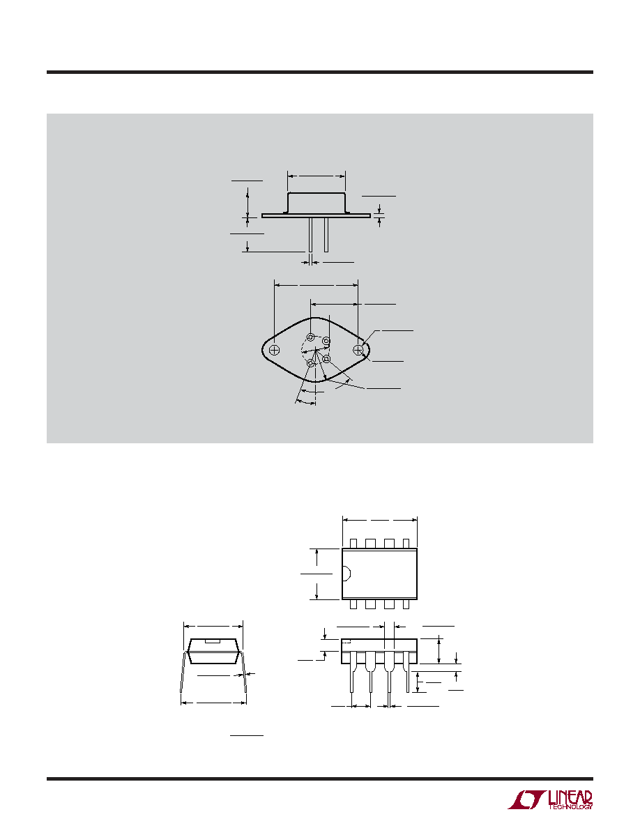
Negative Boost Regulator
J8 Package
8-Lead CERDIP (Narrow .300 Inch, Hermetic)
(Reference LTC DWG # 05-08-1110)
LT1072 ∑ TA13
*REQUIRED IF INPUT LEADS 2"
C2
0.22µF
R3
3.3k
C4
470µF*
V
IN
≠15V
C3
10µF
C1
1000µF
R1
27k
R2
1.24k
R
0
(MINIMUM
LOAD)
D2
D1
V
OUT
≠28V AT 0.25A
L1
200µH
V
IN
V
SW
FB
V
C
GND
LT1072
+
+
+
OBSOLETE PACKAGE
TYPICAL APPLICATIO S
U
U
PACKAGE DESCRIPTIO
14
LT1072
1072fc
K Package
4-Lead TO-3 Metal Can
(Reference LTC DWG # 05-08-1311)
OBSOLETE PACKAGE
K4(TO-3) 1098
72∞
18∞
0.490 ≠ 0.510
(12.45 ≠ 12.95)
R
0.470 TP
P.C.D.
0.167 ≠ 0.177
(4.24 ≠ 4.49)
R
0.151 ≠ 0.161
(3.84 ≠ 4.09)
DIA 2 PLC
0.655 ≠ 0.675
(16.64 ≠ 19.05)
1.177 ≠ 1.197
(29.90 ≠ 30.40)
0.038 ≠ 0.043
(0.965 ≠ 1.09)
0.060 ≠ 0.135
(1.524 ≠ 3.429)
0.320 ≠ 0.350
(8.13 ≠ 8.89)
0.420 ≠ 0.480
(10.67 ≠ 12.19)
0.760 ≠ 0.775
(19.30 ≠ 19.69)
N8 Package
8-Lead PDIP (Narrow .300 Inch)
(Reference LTC DWG # 05-08-1510)
N8 1002
.065
(1.651)
TYP
.045 ≠ .065
(1.143 ≠ 1.651)
.130 ± .005
(3.302 ± 0.127)
.020
(0.508)
MIN
.018 ± .003
(0.457 ± 0.076)
.120
(3.048)
MIN
1
2
3
4
8
7
6
5
.255 ± .015*
(6.477 ± 0.381)
.400*
(10.160)
MAX
.008 ≠ .015
(0.203 ≠ 0.381)
.300 ≠ .325
(7.620 ≠ 8.255)
.325
+.035
≠.015
+0.889
≠0.381
8.255
(
)
NOTE:
1. DIMENSIONS ARE
INCHES
MILLIMETERS
*THESE DIMENSIONS DO NOT INCLUDE MOLD FLASH OR PROTRUSIONS.
MOLD FLASH OR PROTRUSIONS SHALL NOT EXCEED .010 INCH (0.254mm)
.100
(2.54)
BSC
U
PACKAGE DESCRIPTIO
15
LT1072
1072fc
Information furnished by Linear Technology Corporation is believed to be accurate and reliable.
However, no responsibility is assumed for its use. Linear Technology Corporation makes no represen-
tation that the interconnection of its circuits as described herein will not infringe on existing patent rights.
SW Package
16-Lead Plastic Small Outline (Wide .300 Inch)
(Reference LTC DWG # 05-08-1620)
S8 Package
8-Lead Plastic Small Outline (Narrow .150 Inch)
(Reference LTC DWG # 05-08-1610)
U
PACKAGE DESCRIPTIO
.016 ≠ .050
(0.406 ≠ 1.270)
.010 ≠ .020
(0.254 ≠ 0.508)
◊ 45∞
0∞≠ 8∞ TYP
.008 ≠ .010
(0.203 ≠ 0.254)
SO8 0502
.053 ≠ .069
(1.346 ≠ 1.752)
.014 ≠ .019
(0.355 ≠ 0.483)
TYP
.004 ≠ .010
(0.101 ≠ 0.254)
.050
(1.270)
BSC
1
N
2
3
4
N/2
.150 ≠ .157
(3.810 ≠ 3.988)
NOTE 3
8
7
6
5
.189 ≠ .197
(4.801 ≠ 5.004)
NOTE 3
.228 ≠ .244
(5.791 ≠ 6.197)
.245
MIN
N
1
2
3
N/2
.160 ±.005
RECOMMENDED SOLDER PAD LAYOUT
.045 ±.005
.050 BSC
.030 ±.005
TYP
INCHES
(MILLIMETERS)
NOTE:
1. DIMENSIONS IN
2. DRAWING NOT TO SCALE
3. THESE DIMENSIONS DO NOT INCLUDE MOLD FLASH OR PROTRUSIONS.
MOLD FLASH OR PROTRUSIONS SHALL NOT EXCEED .006" (0.15mm)
S16 (WIDE) 0502
NOTE 3
.398 ≠ .413
(10.109 ≠ 10.490)
NOTE 4
16
15
14
13
12
11
10
9
1
N
2
3
4
5
6
7
8
N/2
.394 ≠ .419
(10.007 ≠ 10.643)
.037 ≠ .045
(0.940 ≠ 1.143)
.004 ≠ .012
(0.102 ≠ 0.305)
.093 ≠ .104
(2.362 ≠ 2.642)
.050
(1.270)
BSC
.014 ≠ .019
(0.356 ≠ 0.482)
TYP
0∞ ≠ 8∞ TYP
NOTE 3
.009 ≠ .013
(0.229 ≠ 0.330)
.005
(0.127)
RAD MIN
.016 ≠ .050
(0.406 ≠ 1.270)
.291 ≠ .299
(7.391 ≠ 7.595)
NOTE 4
◊ 45∞
.010 ≠ .029
(0.254 ≠ 0.737)
INCHES
(MILLIMETERS)
NOTE:
1. DIMENSIONS IN
2. DRAWING NOT TO SCALE
3. PIN 1 IDENT, NOTCH ON TOP AND CAVITIES ON THE BOTTOM OF PACKAGES ARE THE MANUFACTURING OPTIONS.
THE PART MAY BE SUPPLIED WITH OR WITHOUT ANY OF THE OPTIONS
4. THESE DIMENSIONS DO NOT INCLUDE MOLD FLASH OR PROTRUSIONS.
MOLD FLASH OR PROTRUSIONS SHALL NOT EXCEED .006" (0.15mm)
.420
MIN
.325 ±.005
RECOMMENDED SOLDER PAD LAYOUT
.045 ±.005
N
1
2
3
N/2
.050 BSC
.030 ±.005
TYP
16
LT1072
1072fc
LW/TP 1102 1K REV C ∑ PRINTED IN USA
LINEAR TECHNOLOGY CORPORATION 1988
Linear Technology Corporation
1630 McCarthy Blvd., Milpitas, CA 95035-7417
(408) 432-1900
FAX: (408) 434-0507
www.linear.com
PART NUMBER
DESCRIPTION
COMMENTS
LT1070/HV
5A I
SW
, 40kHz, High Efficiency Switching Regulator
V
IN
=3V to 40/60V, V
OUT
up to 65/75V, I
Q
=6mA, I
SD
<50µA, TO220-5
Package
LT1071/HV
2.5A I
SW
, 40kHz, High Efficiency Switching Regulator
V
IN
=3V to 40/60V, V
OUT
up to 65/75V, I
Q
=6mA, I
SD
<50µA,TO220-5 Package
LT1082
1A I
SW
, 60kHz, High Efficiency Switching Regulator
V
IN
=3V to 75V, V
OUT
up to 100V, I
Q
=4.5mA, I
SD
<120µA, DD, N8, TO220-5
Packages
LT1170/HV
5A I
SW
, 100kHz, High Efficiency Switching Regulator
V
IN
=3V to 40/60V, V
OUT
up to 65/75V, I
Q
=6mA, I
SD
<50µA, DD, N8, S16,
TO220-5 Packages
LT1171/HV
2.5A I
SW
, 100kHz, High Efficiency Switching
V
IN
=3V to 40/60V, V
OUT
up to 65/75V, I
Q
=6mA, I
SD
<50µA, DD, N8, S16,
Regulator
TO220-5 Packages
LT1172/HV
1.25A I
SW
, 100kHz, High Efficiency Switching
V
IN
=3V to 40/60V, V
OUT
up to 65/75V, I
Q
=6mA, I
SD
<50µA, DD, N8, S16,
Regulator
TO220-5 Packages
LT1307/LT1307B
600mA I
SW
, 600kHz, High Efficiency Switching
V
IN
=1V to 12V, V
OUT
up to 28V, I
Q
=50µA/1mA, I
SD
<1µA, MS8, N8, S8
Regulator
Packages
LT1317/LT1317B
600mA I
SW
, 600kHz, High Efficiency Switching
V
IN
=1.5V to 12V, V
OUT
up to 28V, I
Q
=100µA/4.8mA, I
SD
<30µA/28µA, MS8,
Regulator
S8 Packages
LT1370/HV
6A ISW, 500kHz, High Efficiency Switching Regulator
V
IN
=2.7V to 30V, V
OUT
up to 35/42V, I
Q
=4.5mA, I
SD
<12µA, DD, T0220-7
Packages
LT1371/HV
3A ISW, 500kHz, High Efficiency Switching Regulator
V
IN
=2.7V to 30V, V
OUT
up to 35/42V, I
Q
=4mA, I
SD
<12µA, DD, S20,
T0220-7 Packages
T Package
5-Lead Plastic TO-220 (Standard)
(Reference LTC DWG # 05-08-1421)
U
PACKAGE DESCRIPTIO
RELATED PARTS
T5 (TO-220) 0801
.028 ≠ .038
(0.711 ≠ 0.965)
.067
(1.70)
.135 ≠ .165
(3.429 ≠ 4.191)
.700 ≠ .728
(17.78 ≠ 18.491)
.045 ≠ .055
(1.143 ≠ 1.397)
.095 ≠ .115
(2.413 ≠ 2.921)
.013 ≠ .023
(0.330 ≠ 0.584)
.620
(15.75)
TYP
.155 ≠ .195*
(3.937 ≠ 4.953)
.152 ≠ .202
(3.861 ≠ 5.131)
.260 ≠ .320
(6.60 ≠ 8.13)
.165 ≠ .180
(4.191 ≠ 4.572)
.147 ≠ .155
(3.734 ≠ 3.937)
DIA
.390 ≠ .415
(9.906 ≠ 10.541)
.330 ≠ .370
(8.382 ≠ 9.398)
.460 ≠ .500
(11.684 ≠ 12.700)
.570 ≠ .620
(14.478 ≠ 15.748)
.230 ≠ .270
(5.842 ≠ 6.858)
BSC
SEATING PLANE
* MEASURED AT THE SEATING PLANE