1
LT1076-5
S
FEATURE
U
A
O
PPLICATI
TYPICAL
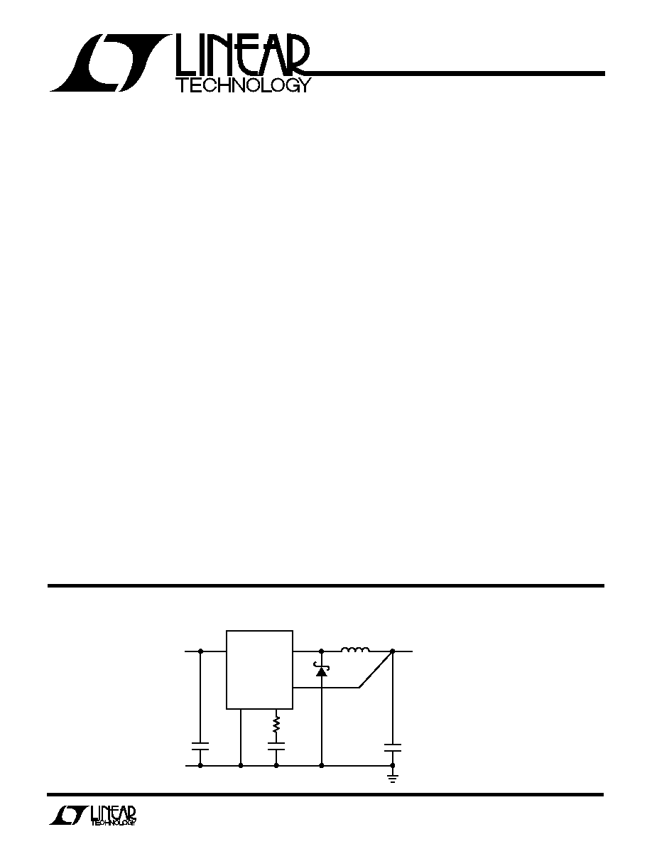
Basic Positive Buck Converter
5V Step-Down
Switching Regulator
D
U
ESCRIPTIO
s
Fixed 5V Output
s
2A On-Board Switch
s
100kHz Switching Frequency
s
2% Output Voltage Tolerance Over Temperature
s
Greatly Improved Dynamic Behavior
s
Available in Low Cost 5-Lead Package
s
Only 9.5mA Quiescent Current
s
Operates Up to 60V Input
s
5V Output Buck Converter
s
Tapped Inductor Buck Converter with 4A Output
at 5V
s
Positive-to-Negative Converter
U
S
A
O
PPLICATI
The LT1076-5 is a 2A fixed 5V output monolithic bipolar
switching regulator which requires only a few external
parts for normal operation. The power switch, all oscillator
and control circuitry, all current limit components, and an
output monitor are included on the chip. The topology is
a classic positive "buck" configuration but several design
innovations allow this device to be used as a positive-to-
negative converter, a negative boost converter, and as a
flyback converter. The switch output is specified to swing
40V below ground, allowing the LT1076-5 to drive a
tapped inductor in the buck mode with output currents up
to 4A.
The LT1076-5 uses a true analog multiplier in the feedback
loop. This makes the device respond nearly instanta-
neously to input voltage fluctuations and makes loop gain
independent of input voltage. As a result, dynamic behav-
ior of the regulator is significantly improved over previous
designs.
On-chip pulse by pulse current limiting makes the LT1076-
5 nearly bust-proof for output overloads or shorts. The
input voltage range as a buck converter is 8V to 60V, but
a self-boot feature allows input voltages as low as 5V in the
inverting and boost configurations.
The LT1076-5 is available in a low cost 5-lead TO-220
package with frequency pre-set at 100kHz and current
limit at 2.6A. See Application Note 44 for design details.
LT1076-5
V
SW
SENSE
V
C
GND
R3
1.5k
C2
0.033
Ķ
F
C3
200
Ķ
F
+
100
Ķ
H**
MBR340*
MBR330P MAY BE USED
FOR V
IN
25V
COILTRONICS #100-1-52
HURRICANE #HL-AG210LL
VALUE MAY BE REDUCED TO 50
Ķ
H
FOR OUTPUT LOADS BELOW 1.5A
8V TO 40V
+
C1
500
Ķ
F
25V
LT1076-5 TA01
V
IN
5V
1.8A
*
**
2
LT1076-5
Input Voltage
LT1076-5 ............................................................ 45V
LT1076HV-5 ....................................................... 64V
Switch Voltage with Respect to Input Voltage
LT1076-5 ............................................................ 64V
LT1076HV-5 ....................................................... 75V
Switch Voltage with Respect to Ground Pin
(V
SW
Negative)
LT1076-5 (Note 5) .............................................. 35V
LT1076HV-5 (Note 5) ......................................... 45V
Sense Pin Voltage ........................................... ≠ 2V, 10V
Maximum Operating Ambient Temperature Range
LT1076C-5, LT1076HVC-5 ..................... 0
į
C to 70
į
C
LT1076I-5, LT1076HVI-5 .................. ≠ 40
į
C to 85
į
C
Maximum Operating Junction Temperature Range
LT1076C-5, LT1076HVC-5 ................... 0
į
C to 125
į
C
LT1076I-5, LT1076HVI-5 ................ ≠ 40
į
C to 125
į
C
Maximum Storage Temperature .......... ≠65
į
C to 150
į
C
Lead Temperature (Soldering, 10 sec).................. 300
į
C
A
U
G
W
A
W
U
W
A
R
BSOLUTE
XI
TI
S
W
U
U
PACKAGE/ORDER I FOR ATIO
PARAMETER
CONDITIONS
MIN
TYP
MAX
UNITS
Switch "On" Voltage (Note 1)
I
SW
= 0.5A
q
1.2
V
I
SW
= 2A
q
1.7
V
Switch "Off" Leakage
V
IN
= 25V, V
SW
= 0
150
Ķ
A
V
IN
= V
MAX
, V
SW
= 0 (Note 6)
250
Ķ
A
Supply Current (Note 2)
V
OUT
= 5.5V, V
IN
40V
q
8.5
11
mA
40V < V
IN
< 60V
q
9.0
12
mA
V
SHDN
= 0.1V (Device Shutdown) (Note 8)
140
300
Ķ
A
Minimum Supply Voltage
Normal Mode
q
7.3
8.0
V
Start-Up Mode (Note 3)
q
3.5
4.8
V
Switch Current Limit (Note 4)
I
LIM
= Open
q
2
2.6
3.2
A
R
LIM
= 10k (Note 9)
1.8
A
R
LIM
= 7k (Note 9)
1.2
A
Maximum Duty Cycle
q
85
90
%
ELECTRICAL C
C
HARA TERISTICS
T
J
= 25
į
C, V
IN
= 25V, unless otherwise noted.
T
JMAX
= 110
į
C
ORDER PART
NUMBER
LT1076CR-5
LT1076CY-5
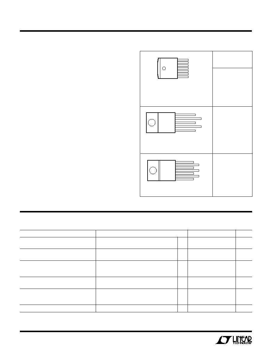
R PACKAGE
7-LEAD PLASTIC DD
FRONT VIEW
SHDN
V
C
SENSE
GND
I
LIM
V
SW
V
IN
7
6
5
4
3
2
1
LT1076CT-5
LT1076HVCT-5
LT1076IT-5
LT1076HVIT-5
FOR STRAIGHT LEADS, ORDER FLOW 06
T
JMAX
= 110
į
C,
JA
= 130
į
C/W
T PACKAGE
5-LEAD TO-220
FRONT VIEW
5
4
3
2
1
V
IN
GND
SENSE
V
SW
V
C
Y PACKAGE
7-LEAD TO-220
SHDN
SENSE
I
LIM
V
IN
V
C
GND
V
SW
FRONT VIEW
7
6
5
4
3
2
1
Consult factory for Military grade parts.
WILL VARY FROM APPROXIMATELY 30
į
C/W WITH
2.8IN
2
OF 1 OZ COPPER TO 70
į
C/W WITH 0.20IN
2
OF
1 OZ COPPER.
T
JMAX
= 110
į
C,
JA
= 130
į
C/W
3
LT1076-5
ELECTRICAL C
C
HARA TERISTICS
T
J
= 25
į
C, V
IN
= 25V, unless otherwise noted.
PARAMETER
CONDITIONS
MIN
TYP
MAX
UNITS
Switching Frequency
90
100
110
kHz
T
J
125
į
C
q
85
120
kHz
V
OUT
= V
SENSE
= 0V (Note 4)
20
kHz
Switching Frequency Line Regulation
8V
V
IN
V
MAX
(Note 7)
q
0.03
0.1
%/ V
Error Amplifier Voltage Gain (Note 7)
1V
V
C
4V
2000
V/ V
Error Amplifier Transconductance (Note 7)
3700
5000
8000
Ķ
mho
Error Amplifier Source and Sink Current
Source (V
SENSE
= 4.5V)
100
140
225
Ķ
A
Sink (V
SENSE
= 5.5V)
0.7
1.0
1.6
mA
Sense Pin Divider Resistance
3
5
8
k
Sense Voltage
V
C
= 2V
q
4.85
5
5.15
V
Output Voltage Tolerance
V
OUT
(Nominal) = 5V
Ī
0.5
Ī
2
%
All Conditions of Input Voltage, Output Voltage,
q
Ī
1.0
Ī
3
%
Temperature and Load Current
Output Voltage Line Regulation
8V
V
IN
V
MAX
(Note 6)
q
0.005
0.02
%/ V
V
C
Voltage at 0% Duty Cycle
1.5
V
Over Temperature
q
≠4.0
mV/
į
C
Multiplier Reference Voltage
24
V
Shutdown Pin Current
V
SHDN
= 5V
5
10
20
Ķ
A
V
SHDN
V
THRESHOLD
(
2.5V)
50
Ķ
A
Shutdown Thresholds
Switch Duty Cycle = 0
2.2
2.45
2.7
V
Fully Shut Down
0.1
0.30
0.5
V
Thermal Resistance Junction to Case
4
į
C/ W
The
q
denotes specifications which apply over the full operating
temperature range.
Note 1: To calculate maximum switch "on" voltage at currents between
low and high conditions, a linear interpolation may be used.
Note 2: A sense pin voltage (V
SENSE
) of 5.5V forces the V
C
pin to its low
clamp level and the switch duty cycle to zero. This approximates the zero
load condition where duty cycle approaches zero.
Note 3: Total voltage from V
IN
pin to ground pin must be
8V after start-
up for proper regulation. For T
A
< 25
į
C, limit = 5V.
Note 4: Switch frequency is internally scaled down when the sense pin
voltage is less than 2.6V to avoid extremely short switch on times. During
current limit testing, V
SENSE
is adjusted to give a minimum switch on time
of 1
Ķ
s.
Note 5: Switch to input voltage limitation must also be observed.
Note 6: V
MAX
= 40V for the LT1076-5 and 60V for the LT1076HV-5.
Note 7: Error amplifier voltage gain and transconductance are specified
relative to the internal feedback node. To calculate gain and
transconductance from the Sense pin (Output) to the V
C
pin, multiply by
0.44.
Note 8: Does not include switch leakage.
Note 9: I
LIM
R
LIM
≠ 1k
5k
Information furnished by Linear Technology Corporation is believed to be accurate and reliable.
However, no responsibility is assumed for its use. Linear Technology Corporation makes no represen-
tation that the interconnection of its circuits as described herein will not infringe on existing patent rights.
4
LT1076-5
Linear Technology Corporation
1630 McCarthy Blvd., Milpitas, CA 95035-7487
(408) 432-1900
q
FAX
: (408) 434-0507
q
TELEX
: 499-3977
©
LINEAR TECHNOLOGY CORPORATION 1994
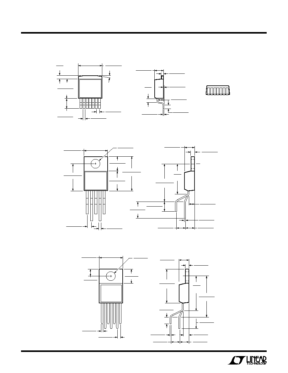
PACKAGE DESCRIPTIO
U
Dimensions in inches (millimeters) unless otherwise noted.
0.147 ≠ 0.155
(3.73 ≠ 3.94)
DIA
0.390 ≠ 0.410
(9.91 ≠ 10.41)
0.045 ≠ 0.055
(1.14 ≠ 1.40)
0.235 ≠ 0.258
(5.97 ≠ 6.55)
0.026 ≠ 0.036
(0.66 ≠ 0.91)
0.103 ≠ 0.113
(2.62 ≠ 2.87)
Y7 0893
0.260 ≠ 0.320
(6.60 ≠ 8.13)
0.045 ≠ 0.055
(1.14 ≠ 1.40)
0.169 ≠ 0.185
(4.29 ≠ 4.70)
0.095 ≠ 0.115
(2.41 ≠ 2.92)
0.155 ≠ 0.195
(3.94 ≠ 4.95)
0.620
(15.75)
TYP
0.560 ≠ 0.590
(14.22 ≠ 14.99)
0.016 ≠ 0.022
(0.41 ≠ 0.56)
0.700 ≠ 0.728
(17.78 ≠ 18.49)
0.135 ≠ 0.165
(3.43 ≠ 4.19)
0.152 ≠ 0.202
(3.86 ≠ 5.13)
R Package, 7-Lead Plastic DD
Y Package, 7-Lead TO-220
LT/GP 0794 5K REV A ∑ PRINTE IN USA
T Package, 5-Lead TO-220
T5 (FORMED) 0694
0.028 ≠ 0.038
(0.711 ≠ 0.965)
0.057 ≠ 0.077
(1.448 ≠ 1.956)
0.135 ≠ 0.165
(3.429 ≠ 4.191)
0.700 ≠ 0.728
(17.780 ≠ 18.491)
0.045 ≠ 0.055
(1.143 ≠ 1.397)
0.095 ≠ 0.115
(2.413 ≠ 2.921)
0.013 ≠ 0.023
(0.330 ≠ 0.584)
0.620
(15.75)
TYP
0.155 ≠ 0.195
(3.937 ≠ 4.953)
0.152 ≠ 0.202
(3.860 ≠ 5.130)
0.260 ≠ 0.320
(6.604 ≠ 8.128)
0.165 ≠ 0.180
(4.293 ≠ 4.572)
0.147 ≠ 0.155
(3.734 ≠ 3.937)
DIA
0.390 ≠ 0.415
(9.906 ≠ 10.541)
0.330 ≠ 0.370
(8.382 ≠ 9.398)
0.460 ≠ 0.500
(11.684 ≠ 12.700)
0.570 ≠ 0.620
(14.478 ≠ 15.748)
0.230 ≠ 0.270
(5.842 ≠ 6.858)
DD7 0693
0.060
(1.524)
0.401 Ī 0.015
(10.185 Ī 0.381)
15į TYP
0.030 Ī 0.008
(0.762 Ī 0.203)
0.331
+0.012
≠0.020
(
)
8.407
+0.305
≠0.508
0.143
+0.012
≠0.020
(
)
3.632
+0.305
≠0.508
0.050 Ī 0.010
(1.270 Ī 0.254)
0.022 Ī 0.005
(0.559 Ī 0.127)
0.105 Ī 0.008
(2.667 Ī 0.203)
0.004
+0.008
≠0.004
(
)
0.102
+0.203
≠0.102
0.050 Ī 0.012
(1.270 Ī 0.305)
0.059
(1.499)
TYP
0.050 Ī 0.008
(1.270 Ī 0.203)
0.175 Ī 0.008
(4.445 Ī 0.203)