 | –≠–ª–µ–∫—Ç—Ä–æ–Ω–Ω—ã–π –∫–æ–º–ø–æ–Ω–µ–Ω—Ç: LT1077A | –°–∫–∞—á–∞—Ç—å:  PDF PDF  ZIP ZIP |
1
LT1077
1077fa
60µA Max Supply Current
40µV Max Offset Voltage
350pA Max Offset Current
0.5µV
P-P
0.1Hz to 10Hz Voltage Noise
2.5pA
P-P
0.1Hz to 10Hz Current Noise
O.4µV/∞C Offset Voltage Drift
250kHz Gain-Bandwidth Product
0.12V/µs Slew Rate
Single Supply Operation
Input Voltage Range Includes Ground
Output Swings to Ground while Sinking Current
No Pull-Down Resistors are Needed
Output Sources and Sinks 5mA Load Current
Replaces OP-07, OP-77, AD707, LT1001, LT1O12
at 10 to 60 Times Lower Power
Battery or Solar Powered Systems
4mA to 2OmA Current Loops
Two Terminal Current Source
Megaohm Source Resistance Difference Amplifier
Micropower, Single Supply,
Precision Op Amp
Self Buffered Micropower Reference
Distribution of Input Offset Voltage
, LTC and LT are registered trademarks of Linear Technology Corporation.
FEATURES
DESCRIPTIO
U
APPLICATIO S
U
TYPICAL APPLICATIO
U
750k
3.6V TO 9V
3
2
0.1µF
LT1034
1.2V
OUTPUT
1.230V
±1.2% MAX
SUPPLY CURRENT = 60µA MAX
SOURCES UP TO 10mA
LOAD REGULATION = 30µV/mA
TEMPERATURE DRIFT = 12ppm/∞C
7
4
6
+
≠
LT1077
LT1077 ∑ TA01
INPUT OFFSET VOLTAGE (µV)
≠40
PERCENT OF UNITS
20
25
30
20
LT1077 ∑ TA02
15
10
≠20
≠30
≠10
0
40
10
30
5
0
35
V
S
= 5V, 0V
T
A
= 25∞C
1072 UNITS
TESTED IN
H, J8, N8
PACKAGES
The LT
Æ
1077 is a micropower precision operational
amplifier optimized for single supply operation at 5V. In
addition, ±15V specifications are provided.
Micropower performance of competing devices is
achieved at the expense of seriously degrading precision,
noise, speed, and output drive specifications. The LT1077
reduces supply current without sacrificing other
parameters. The offset voltage achieved is the lowest
of any micropower op amp. Offset current, voltage
and current noise, slew rate and gain-bandwidth product
are all two to ten times better than on previous micropower
op amps.
The 1/f corner of the voltage noise spectrum is at 0.7Hz.
This results in low frequency (0.1Hz to 10Hz) noise
performance which can only be found on devices with an
order of magnitude higher supply current.
The LT1077 is completely plug-in compatible (including
nulling) with all industry standard precision op amps.
Thus, it can replace these precision op amps in many
applications without sacrificing performance, yet with
significant power savings.
The LT1077 can be operated from one lithium cell or two
Ni-Cad batteries. The input range goes below ground. The
all-NPN output stage swings to ground while sinking
current--no pull-down resistors are needed.
For dual and quad op amps with similar specifications
please see the LT1078/LT1079 datasheet.
2
LT1077
1077fa
LT1077AMH
LT1077MH
LT1077ACH
LT1077CH
LT1077S8
LT1077IS8
LT1077AIN8
LT1077IN8
LT1077ACN8
LT1077CN8
ORDER PART NUMBER
ORDER PART NUMBER
1077
1077I
S8 PART MARKING
TOP VIEW
H PACKAGE
8-LEAD TO-5 METAL CAN
T
JMAX
= 150
∞
C,
JA
= 150
∞
C/W,
JC
= 45
∞
C/W
V
+
V
OS
TRIM
V
OS
TRIM
≠IN
OUT
NC
+IN
V
≠
8
7
5
6
3
2
1
4
A
+
≠
+
≠
B
ORDER PART NUMBER
LT1077AMJ8
LT1077MJ8
LT1077ACJ8
LT1077CJ8
TOP VIEW
J8 PACKAGE
8-LEAD CERDIP
T
JMAX
= 150
∞
C,
JA
= 100
∞
C/W
1
2
3
4
8
7
6
5
V
OS
TRIM
≠IN
+IN
V
≠
V
OS
TRIM
V
+
OUT
NC
LT1077 ∑ POI01
TOP VIEW
N8 PACKAGE
8-LEAD PDIP
S8 PACKAGE
8-LEAD PLASTIC SO
1
2
3
4
8
7
6
5
V
OS
TRIM
V
+
OUT
NC
V
OS
TRIM
≠IN
+IN
V
≠
T
JMAX
= 100
∞
C,
JA
= 130
∞
C/W
T
JMAX
= 150
∞
C,
JA
= 190
∞
C/W
LT1077AM/AI/AC
LT1077M/I/C/S8
SYMBOL
PARAMETER
CONDITIONS
MIN
TYP
MAX
MIN
TYP
MAX
UNITS
V
OS
Input Offset Voltage
9
40
10
60
µV
LT1077S8
12
150
µV
V
OS
Long Term Input Offset
0.4
0.4
µV/Mo
Time
Voltage Stability
I
OS
Input Offset Current
0.06
0.35
0.06
0.45
nA
I
B
Input Bias Current
7
9
7
11
nA
e
n
Input Noise Voltage
0.1Hz to 10Hz (Note3)
0.5
1.1
0.5
µV
P-P
Input Noise Voltage Density
f
O
= 10Hz (Note 3)
28
43
28
nV/Hz
f
O
= 1000Hz (Note3)
27
35
27
nV/Hz
i
n
Input Noise Current
0.1Hz to 10Hz (Note3)
2.5
4.5
2.5
pA
P-P
Supply Voltage ...................................................... ±22V
Differential Input Voltage ....................................... ±30V
Input Voltage ............... Equal to Positive Supply Voltage
Input Voltage ............ 5V Below Negative Supply Voltage
Output Short-Circuit Duration .......................... Indefinite
Consult LTC Marketing for parts specified with wider operating temperature ranges.
V
S
= 5V, 0V, V
CM
= 0.1V, V
O
= 1.4V, T
A
= 25∞C unless noted.
ABSOLUTE AXI U RATI GS
W
W
W
U
PACKAGE/ORDER I FOR ATIO
U
U
W
ELECTRICAL CHARACTERISTICS
Operating Temperature Range
LT1077AM/LT1077M (OBSOLETE).... ≠ 55∞C to 125∞C
LT1077AI/LT1077I .............................. ≠ 40∞C to 85∞C
LT1077AC/LT1077C/LT1077S8 ............... 0∞C to 70∞C
Storage Temperature Range ................. ≠ 65∞C to 150∞C
Lead Temperature (Soldering, 10 sec).................. 300∞C
(Note 1)
OBSOLETE PACKAGE
Consider the N8 or S8 Package for Alternate Source
3
LT1077
1077fa
LT1077AM/AI
LT1077M/I
SYMBOL
PARAMETER
CONDITIONS
MIN
TYP
MAX
MIN
TYP
MAX
UNITS
V
OS
Input Offset Voltage
50
200
60
260
µV
V
OS
/T
Input Offset Voltage Drift
LT1077IS8 (Note 6)
1
2.5
µV/∞C
I
OS
Input Offset Current
0.08
0.60
0.08
0.80
nA
I
B
Input Bias Current
8
11
8
13
nA
CMRR
Common Mode Rejection Ratio
V
CM
= 0.05V to 3.2V
92
104
88
103
dB
PSRR
Power Supply Rejection Ratio
V
S
= 3.1V to 12V
98
114
94
113
dB
A
VOL
Large-Signal Voltage Gain
V
O
= 0.05V to 3.5V, R
L
= 50k
120
600
100
600
V/mV
Maximum Output Voltage
Output Low, No Load
4.5
8
4.5
8
mV
Swing
Output Low, I
SINK
= 100µA
120
170
120
170
mV
Output High, No Load
3.9
4.2
3.9
4.2
V
Output High, 2k to GND
3
3.7
3
3.7
V
I
S
Supply Current
54
80
54
90
µA
LT1077AM/AI/AC
LT1077M/I/C/S8
SYMBOL
PARAMETER
CONDITIONS
MIN
TYP
MAX
MIN
TYP
MAX
UNITS
Input Noise Current Density
f
O
= 10Hz (Note 3)
0.065
0.11
0.065
pA/Hz
f
O
= 1000Hz
0.02
0.02
pA/Hz
Input Resistance
(Note 4)
Differential Mode
350
700
270
700
M
Common Mode
6
6
G
Input Voltage Range
3.5
3.8
3.5
3.8
V
0
≠ 0.3
0
≠ 0.3
V
CMRR
Common Mode Rejection Ratio
V
CM
= 0V to 3.5V
97
106
94
105
dB
PSRR
Power Supply Rejection Ratio
V
S
= 2.3V to 12V
102
118
100
117
dB
A
VOL
Large-Signal Voltage Gain
V
O
= 0.03V to 4V, No Load
300
1000
240
1000
V/mV
V
O
= 0.03V to 3.5V, R
L
= 50k
250
1000
200
1000
V/mV
Maximum Output Voltage
Output Low, No Load
3.5
6
3.5
6
mV
Swing
Output Low, 2k to GND
0.7
1.1
0.7
1.1
mV
Output Low, l
SINK
= 100µA
90
130
90
130
mV
Output High, No Load
4.2
4.4
4.2
4.4
V
Output High, 2k to GND
3.5
3.9
3.5
3.9
V
SR
Slew Rate
(Note 2)
0.05
0.08
0.05
0.08
V/µs
GBW
Gain Bandwidth Product
f
O
20kHz
230
230
kHz
I
S
Supply Current
48
60
48
68
µA
Offset Adjustment Range
R
pot
= 10k, Wiper to V
+
±500
±900
±500
±900
µV
Minimum Supply Voltage
(Note 5)
2.2
2.3
2.2
2.3
V
V
S
= 5V, 0V, V
CM
= 0.1V, V
O
= 1.4V, T
A
= 25∞C unless noted.
ELECTRICAL CHARACTERISTICS
The
denotes the specifications which apply over the temperature range of ≠55∞C T
A
125∞C for AM/M grades,
≠40∞C T
A
85∞C for AI/I grades. V
S
= 5V, 0V, V
CM
= 0.1V, V
O
= 1.4V unless otherwise noted.
4
LT1077
1077fa
LT1077AC
LT1077C/S8
SYMBOL
PARAMETER
CONDITIONS
MIN
TYP
MAX
MIN
TYP
MAX
UNITS
V
OS
Input Offset Voltage
30
110
35
150
µV
LT1077S8
40
280
µV
V
OS
/T
Input Offset Voltage Drift
(Note 6)
0.4
1.6
0.5
2.0
µV/∞C
LT1077S8 (Note 6)
0.7
3.0
µV/∞C
I
OS
Input Offset Current
0.07
0.45
0.07
0.60
nA
I
B
Input Bias Current
7
10
7
12
nA
CMRR
Common Mode Rejection Ratio
V
CM
= 0V to 3.4V
94
105
90
104
dB
PSRR
Power Supply Rejection Ratio
V
S
= 2.6V to 12V
100
116
97
115
dB
A
VOL
Large-Signal Voltage Gain
V
O
= 0.05V to 3.5V, R
L
= 50k
180
800
150
800
V/mV
Maximum Output Voltage Swing
Output Low, No Load
4.0
7
4.0
7
mV
Output Low, I
SINK
= 100µA
100
150
100
150
mV
Output High, No Load
4.1
4.3
4.1
4.3
V
Output High, 2k to GND
3.3
3.8
3.3
3.8
V
I
S
Supply Current
52
70
52
80
µA
The
denotes the specifications which apply over the temperature range
of 0∞C T
A
70∞C otherwise, specifications are at T
A
= 25∞C. V
S
= 5V, 0V, V
CM
= 0.1V, V
O
= 1.4V unless noted.
ELECTRICAL CHARACTERISTICS
LT1077AM/AI/AC
LT1077M/I/C/S8
SYMBOL
PARAMETER
CONDITIONS
MIN
TYP
MAX
MIN
TYP
MAX
UNITS
V
OS
Input Offset Voltage
20
150
25
200
µV
LT1077S8
30
300
µV
I
OS
Input Offset Current
0.06
0.35
0.06
0.45
nA
I
B
Input Bias Current
7
9
7
11
nA
Input Voltage Range
13.5
13.8
13.5
13.8
V
≠ 15.0
≠ 15.3
≠ 15.0
≠ 15.3
V
CMRR
Common Mode Rejection Ratio
V
CM
= 13.5V to ≠15V
100
109
97
108
dB
PSRR
Power Supply Rejection Ratio
V
S
= 5V, 0V to ±18V
106
122
103
120
dB
A
VOL
Large-Signal Voltage Gain
V
O
= ±10V, R
L
= 50k
1000
8000
800
8000
V/mV
V
O
= ±10V, R
L
= 2k
400
1500
300
1500
V/mV
V
OUT
Maximum Output Voltage Swing
R
L
= 50k
±13.0
±14.0
±13.0
±14.0
V
R
L
= 2k
±11.0
±13.2
±11.0
±13.2
V
SR
Slew Rate
0.07
0.12
0.07
0.12
V/µs
I
S
Supply Current
56
75
56
85
µA
V
S
= ±15V, T
A
= 25∞C unless noted.
5
LT1077
1077fa
LT1077AM/AI
LT1077M/I
SYMBOL
PARAMETER
CONDITIONS
MIN
TYP
MAX
MIN
TYP
MAX
UNITS
V
OS
Input Offset Voltage
60
330
75
450
µV
V
OS
/T
Input Offset Voltage Drift
LT1077IS8 (Note 6)
1.1
3
µV/∞C
I
OS
Input Offset Current
0.08
0.60
0.08
0.80
nA
I
B
Input Bias Current
8
11
8
13
nA
A
VOL
Large-Signal Voltage Gain
V
O
= ±10V, R
L
= 5k
300
1000
250
1000
V/mV
CMRR
Common Mode Rejection Ratio
V
CM
= 13V, ≠14.9V
94
107
90
106
dB
PSRR
Power Supply Rejection Ratio
V
S
= 5V, 0V to ±18V
100
118
97
116
dB
Maximum Output Voltage Swing
R
L
= 5k
±11
±13.5
±11
±13.5
V
I
S
Supply Current
60
95
60
105
µA
The
denotes the specifications which apply over the temperature range of
≠55∞C T
A
125∞C for AM/M grades, ≠ 40∞C T
A
85∞C for AI/I grades. V
S
= ±15V unless otherwise noted.
ELECTRICAL CHARACTERISTICS
LT1077AC
LT1077C/S8
SYMBOL
PARAMETER
CONDITIONS
MIN
TYP
MAX
MIN
TYP
MAX
UNITS
V
OS
Input Offset Voltage
40
230
50
320
µV
LT1077S8
65
450
µV
V
OS
/T
Input Offset Voltage Drift
(Note 6)
0.4
1.8
0.5
2.5
µV/∞C
LT1077S8 (Note 6)
0.8
3.5
µV/∞C
I
OS
Input Offset Current
0.07
0.45
0.07
0.60
nA
I
B
Input Bias Current
7
10
7
12
nA
A
VOL
Large-Signal Voltage Gain
V
O
= ±10V, R
L
= 5k
500
2000
400
2000
V/mV
CMRR
Common Mode Rejection Ratio
V
CM
= 13V, ≠15V
97
108
94
107
dB
PSRR
Power Supply Rejection Ratio
V
S
= 5V, 0V to ±18V
103
120
100
118
dB
Maximum Output Voltage Swing
R
L
= 5k
±11
±13.6
±11
±13.6
V
I
S
Supply Current
59
85
59
95
µA
The
denotes the specifications which apply over the temperature range of 0∞C T
A
70∞C.
V
S
= ±15V unless otherwise noted.
Note 1: Absolute Maximum Ratings are those values beyond which the life
of a device may be impared.
Note 2: Slew rate at 5V, 0V is guaranteed by inference from the slew rate
measurement at ±15V.
Note 3: This parameter is tested on a sample basis only. All noise
parameters are tested with V
S
= ± 2.5V, V
O
= 0V.
Note 4: This parameter is guaranteed by design and is not tested.
Note 5: Power supply rejection ratio is measured at the minimum supply
voltage. The op amps actually work at 1.8V supply but with a typical offset
skew of ≠ 300µV.
Note 6: This parameter is not 100% tested.
6
LT1077
1077fa
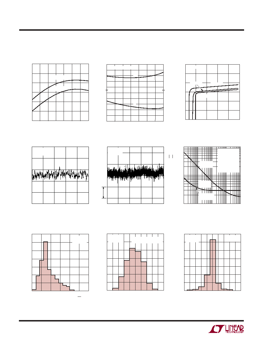
0.1Hz to 10Hz Noise
Supply Current vs Temperature
0.01Hz to 10Hz Noise
Input Bias Currents vs
Common Mode Voltage
Noise Spectrum
10Hz Voltage Noise Distribution
Distribution of Offset Voltage Drift
with Temperature (In All Packages)
Input Bias and Offset Currents
vs Temperature
TYPICAL PERFOR A CE CHARACTERISTICS
U
W
Distribution of Input Offset Voltage
in Small Outline (S8) Package
TEMPERATURE (∞C)
≠50
SUPPLY CURRENT (
µ
A)
60
25
75
LT1077 ∑ TPC01
50
≠25
0
50
100
125
40
V
S
= ±15V
V
S
= 5V, 0V
TEMPERATURE (∞C)
≠50
≠8
BIAS CURRENT (nA)
OFFSET CURRENT (pA)
≠6
50
0
50
75
LT1077 ∑ TPC02
≠7
75
100
≠25
25
100
125
V
S
= 5V, 0V TO ±15V
I
OS
I
B
COMMON MODE VOLTAGE (V)
≠1
≠13
INPUT BIAS CURRENT (nA)
≠11
≠9
≠7
≠5
≠3
≠1
0
1
2
3
LT1077 ∑ TPC03
4
T
A
= 55∞C
T
A
= 125∞C
V
S
= 5V, 0V
T
A
= 25∞C
TIME (SECONDS)
0
NOISE VOLTAGE (0.4
µ
V/DIV)
8
LT1077 ∑ TPC04
2
4
6
10
V
S
= ± 2.5V
T
A
= 2.5∞C
TIME (SECONDS)
0
NOISE VOLTAGE (0.4
µ
V/DIV)
80
LT1077 ∑ TPC05
0.4
µ
V
20
40
60
100
V
S
= ± 2.5V
T
A
= 2.5∞C
FREQUENCY (Hz)
0.1
10
VOLTAGE NOISE DENSITY (nV/
Hz)
CURRNET NOISE DENSITY (fA/
Hz)
100
30
300
1000
10
1000
1
100
LT1077 ∑ TPC06
V
S
= ± 2.5V
T
A
= 25∞C
(AT V
S
= ±15V
VOLTAGE NOISE
IS 4% LESS
CURRENT NOISE
IS UNCHANGED
CURRENT
NOISE
VOLTAGE
NOISE
1/f CORNER
0.7Hz
VOLTAGE NOISE DENSITY (nV/Hz)
25
35
30
25
20
15
10
5
0
LT1077 ∑ TPC07
30
35
40
PERCENT OF UNITS
V
S
= ± 2.5V
T
A
= 2.5∞C
OFFSET VOLTAGE DRIFT WITH TEMPERATURE (nV/∞C)
0
PERCENT OF UNITS
20
≠2.0
0
1.0
LT1077 ∑ TPC08
10
30
2.0
≠1.0
V
S
= 5V, 0V
V
CM
= 0.1V
400 UNITS TESTED
(100 IN EACH PACKAGE)
INPUT OFFSET VOLTAGE (µV)
≠150
0
PERCENT OF UNITS
10
30
40
50
70
≠120
0
60
LT1077 ∑ TPC09
20
60
≠30
120 150
≠90 ≠60
30
90
456 UNITS
TESTED
V
S
= 5V, 0V
T
A
= 25∞C
7
LT1077
1077fa
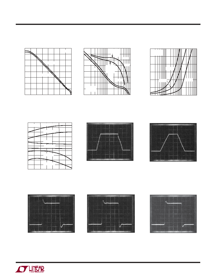
TYPICAL PERFOR A CE CHARACTERISTICS
U
W
Voltage Gain vs Frequency
Large-Signal Transient
Response V
S
= 5V, 0V
Capacitive Load Handling
Large-Signal Transient
Response V
S
= ±15V
Gain, Phase vs Frequency
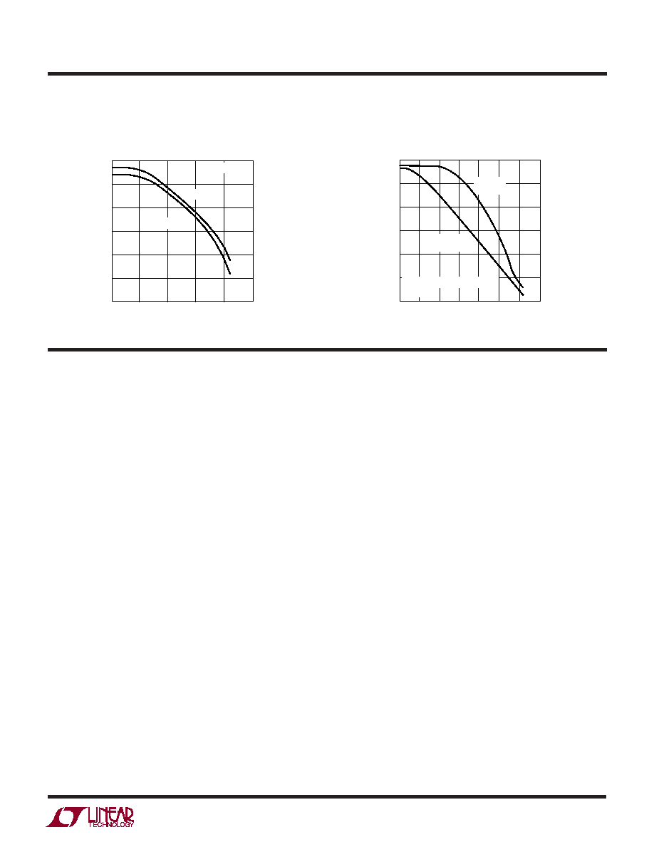
Slew Rate, Gain Bandwidth
Product and Phase Margin vs
Temperature
Small-Signal Transient Response
V
S
= ±
2.5V
Small-Signal Transient Response
V
S
= ±15V
Small-Signal Transient Response
V
S
= 5V, 0V
FREQUENCY (Hz)
0.01
VOLTAGE GAIN (dB)
60
100
1M
LT1077 ∑ TPC10
20
≠20
1
100
10k
0.1
10
1k
100k
140
40
80
0
120
T
A
= 25∞C
V
S
= ±15V
V
S
= 5V, 0V
FREQUENCY (Hz)
10k
30k
≠10
VOLTAGE GAIN (dB)
PHASE SHIFT (DEGREES)
0
10
30
100
120
140
160
180
200
100k
300k
1M
LT1077 ∑ TPC11
20
PHASE
MARGIN
66∞
PHASE
MARGIN
54∞
±15V
±15V
GAIN
5V, 0V
5V, 0V
PHASE
T
A
= 25∞C
C
L
= 20pF
CAPACITIVE LOAD (pF)
10
0
OVERSHOOT (%)
80
100
120
100
1000
10,000
LT1077 ∑ TPC12
60
40
20
V
S
= 5V, 0V
T
A
= 25∞C
A
V
= 1
A
V
= 10
A
V
= 5
TEMPERATURE (∞C)
≠50
180
PHASE MARGIN (DEGREES)
200
240
260
0.14
0.08
0
50
75
LT1077 ∑ TPC13
220
0.10
0.12
0.06
70
80
60
50
40
≠25
25
100
125
SLEW 5V, 0V
M
±15V
GBW 5V, 0V
GBW ±15V
M
±5V, 0V
SLEW ±15V
f
O
= 20kHz
PRODUCT (kHz)
SLEW RATE (V/
µ
s)
GAIN BANDWIDTH
50µs/DIV
1V/DIV
0V
100µs/DIV
5V/DIV
0V
20mV/DIV
10µs/DIV
20mV/DIV
10µs/DIV
20mV/DIV
A
V
= 1
C
L
= 15pF
INPUT 50mV TO 150mV
A
V
= 1
C
L
= 15pF
A
V
= 1
NO LOAD
INPUT PULSE 0V TO 3.8V
A
V
= 1
NO LOAD
0.1V
0V
10µs/DIV
A
V
= 1
C
L
= 15pF
0V
8
LT1077
1077fa
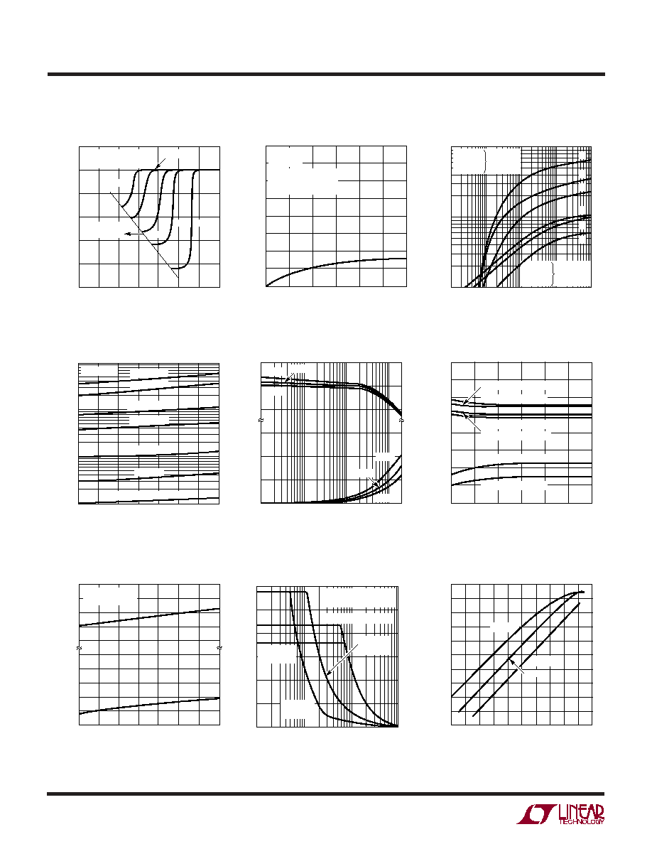
TYPICAL PERFOR A CE CHARACTERISTICS
U
W
Minimum Supply Voltage
Output Voltage Swing vs
Load Current
Voltage Gain vs Load Resistance
Short-Circuit Current vs
Time
Warm-Up Drift
Output Saturation vs Temperature
vs Sink Current
Undistorted Output Swing
vs Frequency
Closed Loop Output
Impedance
Common Mode Range vs
Temperature
POSITIVE SUPPLY VOLTAGE (V)
0
INPUT OFFSET VOLTAGE (
µ
V)
≠100
0
100
LT1077 ∑ TPC19
≠200
≠300
1
2
3
≠400
≠500
V
≠
= 0V
≠ 0.1 V
CM
0.4V
70∞C
25∞C
0∞C
≠ 55∞C
125∞C
NON
FUNCTIONAL
TIME AFTER POWER ON (MINUTES)
0
CHANGE IN OFFSET VOLTAGE (
µ
V)
0.4
LT1077 ∑ TPC20
0.2
0
1
2
0.6
0.8
3
V
S
= ±15V
T
A
= 25∞C
WARM UP DRIFT
AT V
S
= 5V, 0V IS
IMMEASURABLY LOW
LOAD RESISTANCE TO GROUND ()
100
1k
100k
100k
VOLTAGE GAIN (V/V)
1M
10M
10k
1M
LT1077 ∑ TPC21
V
S
= ±15V
1. 25∞C
2. ≠55∞C
3. 125∞C
1
2
3
4
5
6
V
S
= 5V, 0V
4. ≠55∞C
5. 25∞C
6. 125∞C
TEMPERATURE (∞C)
≠50
≠25
SATURATION VOLTAGE (mV)
10
100
1000
0
25
50
75
100
125
LT1077 ∑ TPC22
0
I
SINK
= 1mA
I
SINK
= 100µA
I
SINK
= 10µA
I
SINK
= 1µA
NO LOAD
R
L
= 5k TO GROUND
I
SINK
= 2mA
V
S
= 5V, 0V
SOURCING OR SINKING LOAD CURRENT (mA)
0.01
V
≠
OUTPUT VOLTAGE SWING (V)
V
+
≠ 2
V
+
≠ 1
V
+
0.1
1
10
LT1077 ∑ TPC23
V
≠
+ 2
V
≠
+ 1
≠55∞C
≠55∞C
25∞C
125∞C
125∞C
25∞C
TIME FROM OUTPUT SHORT TO GROUND (MINUTES)
0
SINKING
SOURCING
SHORT-CIRCUIT CURRENT (mA)
≠10
0
10
LT1077 ∑ TPC24
≠20
≠30
≠40
1
2
20
30
40
3
T
A
= 25∞C, V
S
= 5V, 0V
T
A
= 125∞C, V
S
= 5V, 0V
T
A
= 25∞C, V
S
= ±15V
T
A
= 25∞C, V
S
= ±15V
T
A
= 125∞C, V
S
= ±15V
T
A
= 125∞C, V
S
= ±15V
TEMPERATURE (∞C)
≠ 50
0
50
75
LT1077 ∑ TPC25
≠25
25
100
125
V
+
= 2.5V TO 18V
V
≠
= 0V TO ≠18V
V
≠
≠ 1
COMMON MODE RANGE (V)
V
+
≠ 2
V
+
≠ 1
V
+
V
≠
+ 1
V
≠
FREQUENCY (Hz)
100
0
0
1
2
3
4
5
PEAK-TO-PEAK OUTPUT SWING, V
S
=
±
15V (V)
PEAK-TO-PEAK OUTPUT SIWNG, V
S
= 5V, 0V (V)
20
30
1k
10k
100k
LT1077 ∑ TPC26
10
T
A
= 25∞C
LOAD R
L
, TO GROUND
V
S
= 5V, 0V, R
L
100k
V
S
= ±15V
R
L
= 30k
V
S
= ±15V
R
L
100k
V
S
= 5V, 0V
R
L
1k
FREQUENCY (Hz)
OUTPUT IMPEDANCE (
)
100
1k
LT1077 ∑ TPC27
10
1
0.1
10
100
10k
100k
1k
A
V
= 10
A
V
= 1
A
V
= 100
9
LT1077
1077fa
The LT1077 is fully specified with V
+
= 5V, V
≠
= 0V,
V
CM
= 0.1V. This set of operating conditions appears to be
the most representative for battery powered micropower
circuits. Offset voltage is internally trimmed to a minimum
value at these supply voltages. When 9V or 3V batteries,
or ±2.5V dual supplies are used, bias and offset current
changes will be minimal. Offset voltage changes will be
just a few microvolts as given by the PSRR and CMRR
specifications. For example, if PSRR = 114dB ( = 2µV/V),
at 9V the offset voltage change will be 8µV. Similarly,
V
S
±2.5V, V
CM
= 0 is equivalent to a common mode voltage
change of 2.4V or a V
OS
change of 7µV if
CMRR = 110dB (3µV/V).
A full set of specifications is also provided at ±15V supply
voltages for comparison with other devices and for
completeness.
The LT1077 is pin compatible to, and directly replaces,
such precision op amps as the OP-07, OP-77, AD7O7 and
LT1001 with 30 to 60 times savings in supply current. The
LT1077 is also a direct plug-in replacement for LT1012
and OP-97 devices with 10 times lower dissipation.
Compatibility includes externally nulling the offset
voltage, as all of the devices above are trimmed with
a potentiometer between Pins 1 and 8 and the wiper
tied to V
+
.
The LT1077 replaces and upgrades such micropower op
amps as the OP-20, LM4250, and OP-90, provided that the
external nulling circuitry (and set resistor in the case of the
LM4250) are removed. Since the offset voltage of the
LT1077 is extremely low, nulling will be unnecessary in
most applications.
Single Supply Operation
The LT1077 is fully specified for single supply operation,
(i.e., when the negative supply is 0V). Input common
mode range goes below ground and the output swings
within a few millivolts of ground while sinking current. All
competing micropower op amps either cannot swing to
within 600mV of ground (OP-20, OP-220, OP-420) or
need a pull-down resistor connected to the output to
swing to ground (OP-90, OP-290, OP-490, HA5141/42/
44). This difference is critical because in many applica-
tions these competing devices cannot be operated as
micropower op amps and swing to ground simultaneously.
Consider the difference amplifiers shown in Typical
Applications as an example. When the common mode
signal is high and the output low, the amplifier has to sink
current. In the gain of 10 circuit, the competing devices
require a 30k pull-down resistor at the output to handle the
specified signals. (The LT1077 does not need pull-down
TYPICAL PERFOR A CE CHARACTERISTICS
U
W
Common Mode Rejection Ratio
vs Frequency
Power Supply Rejection Ratio
vs Frequency
FREQUENCY (Hz)
10
0
COMMON MODE REJECTION RATIO (dB)
20
40
60
80
100
120
100
1k
10k
100k
LT1077 ∑ TPC28
1M
T
A
= 25∞C
V
S
= ±15V
V
S
= 5V, 0V
FREQUENCY (Hz)
0.1
POWER SUPPLY REJECTION RATIO (dB)
80
100
120
100
10k
LT1077 ∑ TPC29
60
40
1
10
1k
100k
20
0
POSITIVE
SUPPLY
NEGATIVE
SUPPLY
V
S
= ± 2.5V + 1V
P-P
SINE WAVE
T
A
= 25∞C
APPLICATIO S I FOR ATIO
W
U
U
U
10
LT1077
1077fa
APPLICATIO S I FOR ATIO
W
U
U
U
resistors.) When the output is high the pull-down resistor
draws 80µA which dominates the micropower current
budget. This situation is much worse in the gain of one
circuit with V
≠
=0V. At 100V common mode, the output has
to sink 2µA. At a minimum output voltage of 20mV
competing devices require a 10k pull-down resistor. As
the output now swings to 10V, this resistor draws 1mA of
current.
Since the output of the LT1077 cannot go exactly to
ground, but can only approach ground to within a few
millivolts, care should be exercised to ensure that the
output is not saturated. For example, a 1mV input signal
will cause the amplifier to set up in its linear region in the
gain 100 configuration shown below; however, it is not
enough to make the amplifier function properly in the
voltage follower mode.
Voltage Follower with Input Exceeding the Negative Common Mode Range (V
S
= 5V, 0V)
Single supply operation can also create difficulties at the
input. The driving signal can fall below 0V--inadvertently
or on a transient basis. If the input is more than a few
hundred millivolts below ground, two distinct problems
can occur on previous single supply designs, such as the
LM124, LM158, OP-20, OP-21, OP-220, OP-221, OP-420
(a and b), OP-90/290/490 (b only):
a) When the input is more than a diode drop below
ground, unlimited current will flow from the substrate
(V
≠
terminal) to the input (this can destroy the unit). On the
LT1077, resistors in series with the input protect the
device even when the input is 5V below ground.
b) When the input is more than 400mV below ground
(at 25∞C), the input stage saturates and phase reversal
occurs at the output (this can cause lock-up in servo
systems). Due to a unique phase reversal protection
circuitry, the LT1077's output does not reverse, as
illustrated below, even when the input is at ≠ 1.0V.
100mV
1mV
99R
5V
R
+
≠
OUTPUT
SATURATED
3.5mV
1mV
5V
+
≠
LT1077 ∑ AI01
Gain 100 Amplifier
Voltage Follower
1ms/DIV
2V
1ms/DIV
2V
2V
4V
4V
4V
0
0
0
LT1077
NO PHASE REVERSAL
OP-90
EXHIBITS OUTPUT
PHASE REVERSAL
1ms/DIV
6V
P-P
INPUT
≠1.0 TO 5.0V
11
LT1077
1077fa
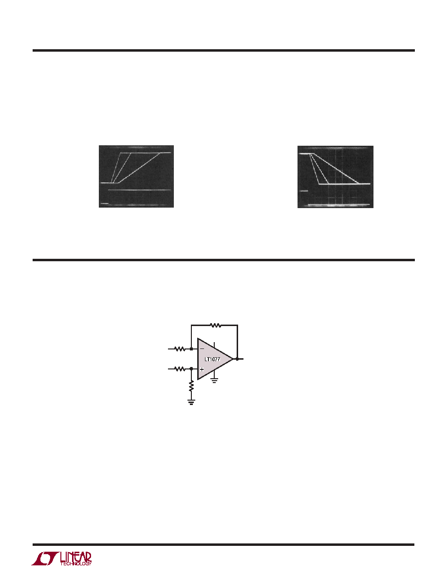
Comparator Applications
The single supply operation of the LT1077 and its
ability to swing close to ground while sinking current,
Comparator Rise Response Time
to 10mV, 5mV, 2mV Overdrive
Comparator Fall Response Time
to 10mV, 5mV, 2mV Overdrive
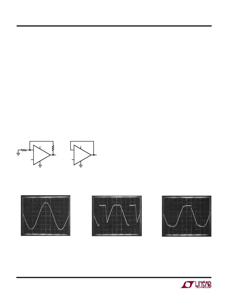
TYPICAL APPLICATIO S
U
Megaohm Input Impedance
Gain of 10 Difference Amplifier
OUTPUT
0.005 TO 2.4V
BANDWIDTH =
OUTPUT OFFSET =
OUTPUT NOISE =
SUPPLY CURRENT =
20KHZ
0.7mV
80µVPP (0.1Hz TO 10Hz)
260µV
RMS
OVER FULL BANDWIDTH
45µA
THE USEFULNESS OF DIFFERENCE AMPLIFIERS IS LIMITED BY THE FACT
THAT THE INPUT RESISTANCE IS EQUAL TO THE SOURCE RESISTANCE.
THE PICO-AMPERE OFFSET CURRENT AND LOW CURRENT NOISE OF THE LT1077
ALLOWS THE USE OF 1M SOURCE RESISTORS WITHOUT DEGRADATION IN
PERFORMANCE. IN ADDITION, WITH MEGAOHM RESISTORS MICROPOWER
OPERATION CAN BE MAINTAINED
6
7
4
2
3
3V
10M
10M
1M
1M
INPUT
≠
+
LT1077 ∑ TA03
lends itself to use as a precision comparator with
TTL compatible output.
200µs/DIV
OUTPUT (V)
0
0
2
4
≠100
INPUT (mV)
200µs/DIV
OUTPUT (V)
0
0
2
4
100
INPUT (mV)
V
S
= 5V, 0V
V
S
= 5V, 0V
APPLICATIO S I FOR ATIO
W
U
U
U
12
LT1077
1077fa
±250V Common Mode Range Difference Amplifier (A
V
= 1)
Two Terminal Current Source
Half-Wave Rectifier
TYPICAL APPLICATIO S
U
COMMON MODE REJECTION RATIO =
WITH OPTIONAL TRIM =
OUTPUT OFFSET (TRIMMABLE TO ZERO) =
OUTPUT OFFSET DRIFT =
INPUT RESISTANCE =
COMMON MODE RANGE =
=
=
74dB (RESISTOR LIMITED)
108dB
500µV
25µV/∞C
1M
± 250V, V
+
= 6.2V TO 18V, V
≠
= ≠ 4.7V TO ≠18V
± 100V, V
+
+
3.2V, V
≠
≠1.8V
100V, ≠13V, V
+
3.2V, V
≠
= 0V
COMMON
MODE
INPUT
± 250V
+ IN
≠ IN
R3
1M
R1
1M
R5
975k
R2
20k
OUT
50k
OPTIONAL
CMRR
TRIM
R1 TO R6: VISHAY 444 ACCUTRACT THIN FILM
SIP NETWORK
:VISHAY 444 PIN NUMBERS
VISHAY INTERTECHNOLOGY, INC.
63 LINCOLN HIGHWAY
MALVERN, PA 19355
R6
25k
R4
19.608k
3V TO 18V
OV TO ≠18V
2
7
4
6
3
X
5
6
7
4
1
2
3
LT1077 ∑ TA04
+
≠
LT1077
4
7
6
3.6V TO 40V
MINIMUM CURRENT = 50µA (R1 )
MAXIMUM CURRENT = 10.3mA (R1 = 120)
LT1034
1.2V
750k
R
L
I
S
I
O
I
O
=
+ I
S
V
R1
R
1
R1
V
R1
+
≠
2
3
=
+ 50µA
1.230V
R
1
LT1077 ∑ TA05
+
≠
OUTPUT
1.8V
1.8V
≠1.8V
0
V
0MIN
= 6mV
NO DISTORTION TO 100Hz
LT1077
3V
2M
1M
1M
INPUT
LT1077 ∑ TA06
13
LT1077
1077fa
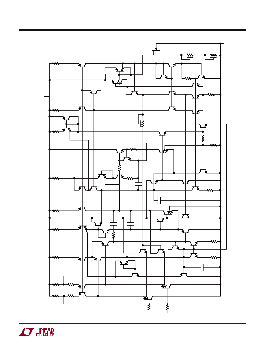
SI PLIFIED SCHE ATIC
W
W
700k
700k
9.1k
5.35k
Q43
Q51
Q50
Q48
Q44
Q42
Q55
Q49
Q45
V
≠
V
+
V
+
V
+
V
+
V
≠
J1
Q52
Q46
Q53
2
1
1
12.5k
11.5k
3.6k
30
OUT
150k
2.9k
5.6k
2.2k
700
NULL
NULL
700
9k
9k
1.3k
Q41
Q40
Q54
Q47
Q32
Q37
Q30
1
3
Q15
Q14
Q6
Q16
Q5
5k
Q3
Q4
Q24
8.6k
600
≠IN
3k
Q12
Q1
Q21
Q2
Q22
4
1
Q1
Q29
C1
50pF
C5
2.5pF
C4
4pF
C3
40pF
Q25
Q26
Q35
Q33
Q31
Q19
Q23
Q36
C2
175pF
Q18
Q27
Q28
Q39
Q8
6.2k
10k
1.35k
30
6.2k
Q7
600
+IN
Q9
Q17
Q10
Q38
Q34
Q20
LT1077 ∑ S01
14
LT1077
1077fa
U
PACKAGE DESCRIPTIO
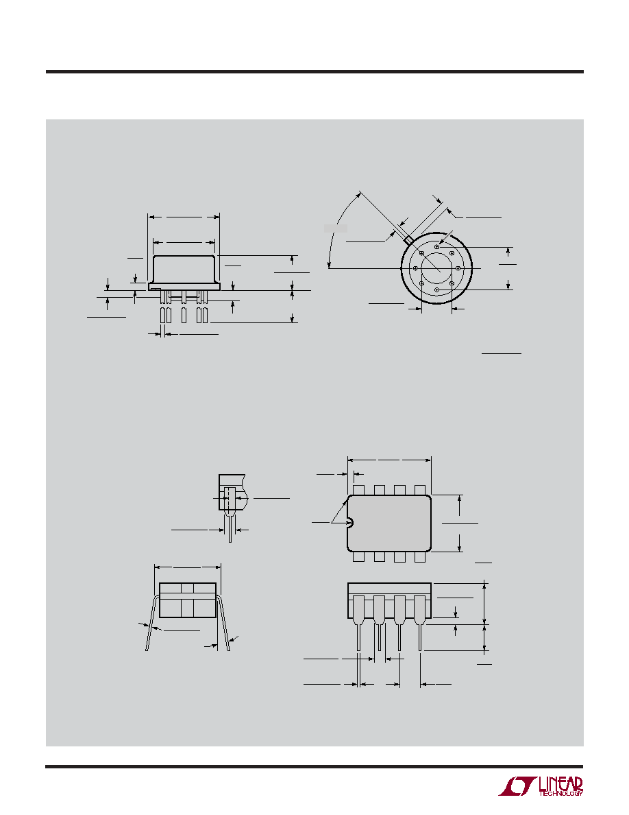
H Package
8-Lead TO-5 Metal Can (.200 Inch PCD)
(Reference LTC DWG # 05-08-1320)
OBSOLETE PACKAGES
J8 Package
8-Lead CERDIP (Narrow .300 Inch, Hermetic)
(Reference LTC DWG # 05-08-1110)
J8 0801
.014 ≠ .026
(0.360 ≠ 0.660)
.200
(5.080)
MAX
.015 ≠ .060
(0.381 ≠ 1.524)
.125
3.175
MIN
.100
(2.54)
BSC
.300 BSC
(7.62 BSC)
.008 ≠ .018
(0.203 ≠ 0.457)
0∞ ≠ 15∞
.005
(0.127)
MIN
.405
(10.287)
MAX
.220 ≠ .310
(5.588 ≠ 7.874)
1
2
3
4
8
7
6
5
.025
(0.635)
RAD TYP
.045 ≠ .068
(1.143 ≠ 1.650)
FULL LEAD
OPTION
.023 ≠ .045
(0.584 ≠ 1.143)
HALF LEAD
OPTION
CORNER LEADS OPTION
(4 PLCS)
.045 ≠ .065
(1.143 ≠ 1.651)
NOTE: LEAD DIMENSIONS APPLY TO SOLDER DIP/PLATE
OR TIN PLATE LEADS
.050
(1.270)
MAX
.016 ≠ .021**
(0.406 ≠ 0.533)
.010 ≠ .045*
(0.254 ≠ 1.143)
SEATING
PLANE
.040
(1.016)
MAX
.165 ≠ .185
(4.191 ≠ 4.699)
GAUGE
PLANE
REFERENCE
PLANE
.500 ≠ .750
(12.700 ≠ 19.050)
.305 ≠ .335
(7.747 ≠ 8.509)
.335 ≠ .370
(8.509 ≠ 9.398)
DIA
.200
(5.080)
TYP
.027 ≠ .045
(0.686 ≠ 1.143)
.028 ≠ .034
(0.711 ≠ 0.864)
.110 ≠ .160
(2.794 ≠ 4.064)
INSULATING
STANDOFF
45∞TYP
H8(TO-5) 0.200 PCD 0801
LEAD DIAMETER IS UNCONTROLLED BETWEEN THE REFERENCE PLANE
AND THE SEATING PLANE
FOR SOLDER DIP LEAD FINISH, LEAD DIAMETER IS
.016 ≠ .024
(0.406 ≠ 0.610)
*
**
PIN 1
15
LT1077
1077fa
Information furnished by Linear Technology Corporation is believed to be accurate and reliable.
However, no responsibility is assumed for its use. Linear Technology Corporation makes no represen-
tation that the interconnection of its circuits as described herein will not infringe on existing patent rights.
U
PACKAGE DESCRIPTIO
N8 0502
.100
(2.54)
BSC
.065
(1.651)
TYP
.045 ≠ .065
(1.143 ≠ 1.651)
.130 ± .005
(3.302 ± 0.127)
.020
(0.508)
MIN
.018 ± .003
(0.457 ± 0.076)
.125
(3.175)
MIN
1
2
3
4
8
7
6
5
.255 ± .015*
(6.477 ± 0.381)
.400*
(10.160)
MAX
.009 ≠ .015
(0.229 ≠ 0.381)
.300 ≠ .325
(7.620 ≠ 8.255)
.325
+.035
≠.015
+0.889
≠0.381
8.255
(
)
NOTE:
1. DIMENSIONS ARE
INCHES
MILLIMETERS
*THESE DIMENSIONS DO NOT INCLUDE MOLD FLASH OR PROTRUSIONS.
MOLD FLASH OR PROTRUSIONS SHALL NOT EXCEED .010 INCH (0.254mm)
N8 Package
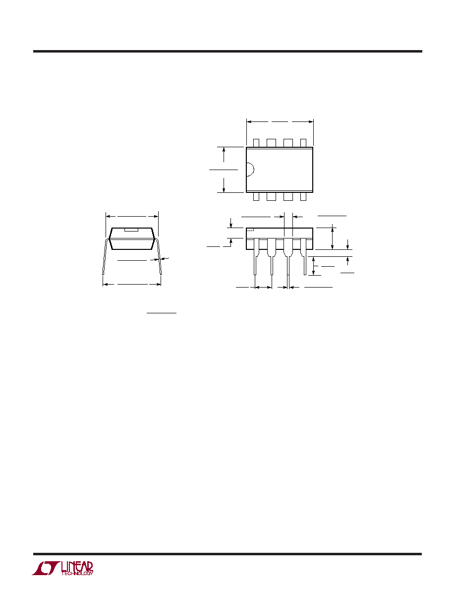
8-Lead PDIP (Narrow .300 Inch)
(Reference LTC DWG # 05-08-1510)
16
LT1077
1077fa
Linear Technology Corporation
1630 McCarthy Blvd., Milpitas, CA 95035-7417
(408) 432-1900
FAX: (408) 434-0507
www.linear.com
LW/TP 1002 1K REV A ∑ PRINTED IN USA
LINEAR TECHNOLOGY CORPORATION 1989
U
PACKAGE DESCRIPTIO
.016 ≠ .050
(0.406 ≠ 1.270)
.010 ≠ .020
(0.254 ≠ 0.508)
◊ 45∞
0∞≠ 8∞ TYP
.008 ≠ .010
(0.203 ≠ 0.254)
SO8 0502
.053 ≠ .069
(1.346 ≠ 1.752)
.014 ≠ .019
(0.355 ≠ 0.483)
TYP
.004 ≠ .010
(0.101 ≠ 0.254)
.050
(1.270)
BSC
1
N
2
3
4
N/2
.150 ≠ .157
(3.810 ≠ 3.988)
NOTE 3
8
7
6
5
.189 ≠ .197
(4.801 ≠ 5.004)
NOTE 3
.228 ≠ .244
(5.791 ≠ 6.197)
.245
MIN
N
1
2
3
N/2
.160 ±.005
RECOMMENDED SOLDER PAD LAYOUT
.045 ±.005
.050 BSC
.030 ±.005
TYP
INCHES
(MILLIMETERS)
NOTE:
1. DIMENSIONS IN
2. DRAWING NOT TO SCALE
3. THESE DIMENSIONS DO NOT INCLUDE MOLD FLASH OR PROTRUSIONS.
MOLD FLASH OR PROTRUSIONS SHALL NOT EXCEED .006" (0.15mm)
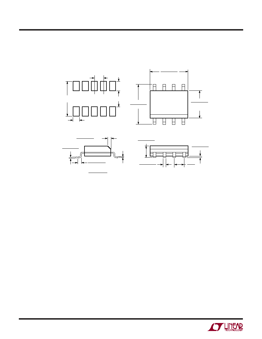
S8 Package
8-Lead Plastic Small Outline (Narrow .150 Inch)
(Reference LTC DWG # 05-08-1610)