 | –≠–ª–µ–∫—Ç—Ä–æ–Ω–Ω—ã–π –∫–æ–º–ø–æ–Ω–µ–Ω—Ç: LT1082CQ | –°–∫–∞—á–∞—Ç—å:  PDF PDF  ZIP ZIP |
1
LT1082
1A High Voltage, Efficiency
Switching Voltage Regulator
LT1082C
LT1072HV
V
IN
3V to 75V
3V to 60V
V
SW
100V
75V
Switch Current Limit
1A
1.25A
Quiescent Current
4.5mA
6mA
Operating Frequency
60kHz
40kHz
Flyback Reference Voltage
16.2 + 0.6 (35k
/R
FB
) 16 + 0.35 (7k
/R
FB
)
LT1082 and LT1072 Major Specification Differences
USER NOTE: This data sheet is only intended to provide specifications, graphs, and a general
functional description of the LT1082. Application circuits are included to show the capability of the
LT1082. A complete design manual (AN19) and Switcher CAD (LTC Switching Power Supply Design
Program) should be obtained to assist in developing new designs. This manual contains a
comprehensive discussion of both the LT1070 and the external components used with it, as well as
complete formulas for calculating the values of these components. The manual can also be used for
the LT1082 by factoring in the lower switch current rating.
s
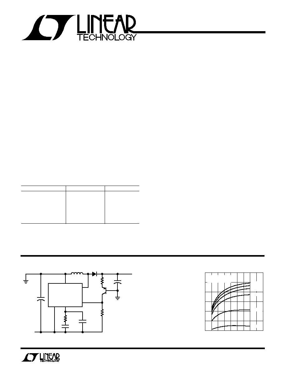
Telecom 5V Supply at 0.7A from ≠48V
s
90V Supply at 120mA from 15V
s
All Applications Using LT1072 (See Below for
Specification Differences)
U
S
A
O
PPLICATI
S
FEATURE
s
Wide Input Voltage Range: 3V to 75V
s
High Switch Voltage: 100V
s
Low Quiescent Current: 4.5mA
s
Internal 1A Switch
s
Shutdown Mode Draws Only 120
µ
A Supply Current
s
Isolated Flyback Regulation Mode for Fully Floating
Outputs
s
Can Be Externally Synchronized
s
Available in MiniDIP and TO-220 Packages
s
Same Pinout as LT1072
The LT1082 is a monolithic high voltage switching
regulator. It can be operated in all standard switching
configurations including buck, boost, flyback, forward,
and inverting. A 1A high efficiency switch is included on
the die along with all oscillator, control, and protection
circuitry.
The LT1082 operates with supply voltages from 3V to 75V,
switch voltage up to 100V and draws only 4.5mA quies-
cent current. It can deliver load power up to 20W with no
external power devices. By utilizing current-mode switch-
ing techniques, it provides excellent AC and DC load and
line regulation.
An externally activated shutdown mode reduces total
supply current to 120
µ
A typical for standby operation.
Totally isolated and regulated outputs can be generated by
using the optional "isolated flyback regulation mode" built
into the LT1082, without the need for optocouplers or
extra transformer windings.
The LT1082 has a unique feature to provide high voltage
short-circuit protection. When the FB pin is pulled down to
0.6V and the current out of the pin reaches approximately
350
µ
A, the switching frequency will shift down from
60kHz to 12kHz.
The LT1082 is nearly identical to the lower voltage LT1072.
For the major differences in specifications, see the table on
the left.
D
U
ESCRIPTIO
Negative-to-Positive Telecom 5V Supply
INPUT VOLTAGE (V)
0
MAXIMUM OUTPUT CURRENT (A)
≠20
≠40 ≠50
≠90
1082 TA02
≠10
≠30
≠60 ≠70 ≠80
1.0
0.9
0.8
0.7
0.6
0.5
0.4
L=550
µ
H
L=450
µ
H
L=350
µ
H
L=250
µ
H
L=150
µ
H
L=100
µ
H
f = 45kHz
I
SW
LIMIT = 1.07A
Telecom 5V Supply Maximum Output
Current vs Input Voltage
+
V
IN
V
SW
GND
FB
V
C
LT1082
4.7k
0.22
µ
F
33
µ
F
80V
CHEMI-CON
SXE SERIES
≠20V
TO ≠70V
**250
µ
H
3.83k
+
0.01
µ
F
1.1k
Q1
2N5401
470
µ
F
10V
CHEMI-CON
SXE SERIES
V
OUT
5V, 0.7A
*D1
MOTOROLA MUR110 (100V, 1A)
69 TURNS OF #28 AWG WIRE ON A
MICROMETALS T60 TYPE 52 CORE.
NOTE: THIS CORE IS LOW COST, BUT
HAS HIGHER CORE LOSS AND IS LARGER
THAN NECESSARY FOR LOWER CURRENT
APPLICATIONS. FOR SMALLER INDUCTORS
OR HIGHER EFFICIENCY, USE A LOW LOSS
CORE SUCH AS MAGNETICS INC. KOOL M
µ
OR MOLYPERMALLOY.
*
**
1082 TA01
NOTE: MAXIMUM OUTPUT
CURRENT IS A FUNCTION
OF INPUT VOLTAGE. SEE
THE GRAPH ON THE RIGHT.
2
LT1082
A
U
G
W
A
W
U
W
A
R
BSOLUTE
XI
TI
S
Supply Voltage ....................................................... 75V
Switch Output Voltage .......................................... 100V
Feedback Pin Voltage (Transient, 1ms) ................
±
15V
Storage Temperature Range ................ ≠ 65
∞
C to 150
∞
C
Lead Temperature (Soldering, 10 sec)................. 300
∞
C
Operating Junction Temperature Range
LT1082M ......................................... ≠ 55
∞
C to 150
∞
C
LT1082I ........................................... ≠ 40
∞
C to 125
∞
C
LT1082C ............................................... 0
∞
C to 100
∞
C
ELECTRICAL C
C
HARA TERISTICS
SYMBOL
PARAMETER
CONDITIONS
MIN
TYP
MAX
UNITS
V
REF
Reference Voltage
Measured at Feedback Pin
1.224 1.244
1.264
V
V
C
= 0.8V
q
1.214 1.244
1.274
V
I
B
Feedback Input Current
V
FB
= V
REF
350
750
nA
q
1100
nA
g
m
Error Amplifier
I
C
=
±
25
µ
A
3000
4400
6000
µ
mho
Transconductance
q
2400
7000
µ
mho
Error Amplifier Source or
V
C
= 1.5V
150
200
400
µ
A
Sink Current
q
120
400
µ
A
Error Amplifier Clamp
Hi Clamp, V
FB
= 1V
1.8
2.3
V
Voltage
Lo Clamp, V
FB
= 1.5V
0.12
0.22
0.36
V
Reference Voltage Line Regulation
3V
V
IN
V
MAX
, V
C
= 0.8V
q
0.03
%/V
A
V
Error Amplifier Voltage Gain
0.9V
V
C
1.4V
350
650
V/V
Minimum Input Voltage
q
2.6
3.0
V
V
IN
= 15V, V
C
= 0.5V, V
FB
= V
REF
, output pin open, unless otherwise specified.
1
2
3
4
8
7
6
5
TOP VIEW
GND
V
C
FB
NC
E2
V
SW
E1
V
IN
N8 PACKAGE
8-LEAD PLASTIC DIP
J8 PACKAGE
8-LEAD CERAMIC DIP
Q PACKAGE
5-LEAD DD
V
IN
V
SW
GND
FB
V
C
FRONT VIEW
5
4
3
2
1
T PACKAGE
5-LEAD TO-220
V
IN
V
SW
GND
FB
V
C
FRONT VIEW
5
4
3
2
1
T
JMAX
= 150
∞
C,
JA
= 100
∞
C/W (MJ8)
T
JMAX
= 100
∞
C,
JA
= 90
∞
C/W (CN8)
T
JMAX
= 125
∞
C,
JA
= 90
∞
C/W (IN8)
T
JMAX
= 100
∞
C,
JA
= 40
∞
C/ W (CQ)
T
JMAX
= 125
∞
C,
JA
= 40
∞
C/ W (IQ)
NOTE:
JA
VARIES FROM 25
∞
C/W TO 50
∞
C/W
DEPENDING ON BOARD COMPOSITION.
T
JMAX
= 100
∞
C,
JA
= 75
∞
C/ W,
JC
= 8
∞
C/ W (CT)
T
JMAX
= 125
∞
C,
JA
= 75
∞
C/ W,
JC
= 8
∞
C/ W (IT)
W
U
U
PACKAGE/ORDER I FOR ATIO
ORDER PART NUMBER
ORDER PART NUMBER
ORDER PART NUMBER
LT1082MJ8
LT1082CN8
LT1082IN8
LT1082CQ
LT1082IQ
LT1082CT
LT1082IT
3
LT1082
ELECTRICAL C
C
HARA TERISTICS
V
IN
= 15V, V
C
= 0.5V, V
FB
= V
REF
, output pin open, unless otherwise specified.
SYMBOL
PARAMETER
CONDITIONS
MIN
TYP
MAX
UNITS
I
Q
Supply Current
3V
V
IN
V
MAX
, V
C
= 0.6V
4.5
7.0
mA
Control Pin Threshold
Duty Cycle = 0
0.7
0.9
1.1
V
q
0.5
1.25
V
Normal/Flyback Threshold
0.58
0.67
0.8
V
on Feedback Pin
f
Switching Frequency
50
60
70
kHz
q
45
75
kHz
800
µ
A
I
FB
450
µ
A
12
kHz
BV
Output Switch Breakdown Voltage
3V
V
IN
V
MAX
, I
SW
= 1.5mA
q
100
115
V
Control Voltage to Switch
1.5
A/V
Current Transconductance
V
FB
Flyback Reference Voltage
I
FB
= 60
µ
A
17
18.6
20.5
V
q
16
21.5
V
Change in Flyback Reference Voltage
60
µ
A
I
FB
200
µ
A
3.5
4.6
6.5
V
Flyback Reference Voltage Line Regulation
I
FB
= 60
µ
A, 3V
V
IN
V
MAX
0.01
0.03
%/V
Flyback Amplifier Transconductance (g
m
)
I
C
=
±
10
µ
A
150
300
500
µ
mho
Flyback Amplifier Source
V
C
= 0.6V Source
q
15
32
70
µ
A
and Sink Current
I
FB
= 60
µ
A Sink
q
30
50
90
µ
A
V
SAT
Output Switch "On" Resistance (Note 1)
I
SW
= 0.7A (LT1082C), I
SW
= 0.5A (LT1082M)
q
0.8
1.2
I
LIM
Switch Current Limit
Duty Cycle = 20%
q
1.07
2.6
A
(LT1082C)
Duty Cycle
50%
q
1.0
2.6
A
Duty Cycle = 80% (Note 2)
q
0.8
2.4
A
Switch Current Limit
Duty Cycle = 20%
q
0.85
2.8
A
(LT1082I)
Duty Cycle
50%
q
0.8
2.8
A
Duty Cycle = 80% (Note 2)
q
0.65
2.6
A
Switch Current Limit
Duty Cycle = 20%
q
0.75
3.0
A
(LT1082M)
Duty Cycle
50%
q
0.7
3.0
A
Duty Cycle = 80% (Note 2)
q
0.6
2.8
A
I
IN
Supply Current Increase
35
45
mA/A
I
SW
During Switch-On Time
DC
MAX
Maximum Switch Duty Cycle
85
92
97
%
Flyback Sense Delay Time
1.5
µ
s
Shutdown Mode Supply Current
3V
V
IN
V
MAX
, V
C
= 0.05V
120
350
µ
A
Shutdown Mode
3V
V
IN
V
MAX
70
150
250
mV
Threshold Voltage
q
50
300
mV
The
q
denotes the specifications which apply over the operating
temperature range.
Note 1: Measured with V
C
in hi clamp, V
FB
= 0.8V.
Note 2: For duty cycles (DC) between 50% and 80%, minimum
guaranteed switch current decreases linearly.
4
LT1082
C
C
HARA TERISTICS
U
W
A
TYPICAL PERFOR
CE
Suggested Core Size and
Inductance for Telecom
5V Supply
Telecom 5V Supply Short-Circuit
Frequency Shift-Down
Minimum Input Voltage
TEMPERATURE (∞C)
≠75
MINIMUM INPUT VOLTAGE (V)
2.9
2.8
2.7
2.6
2.5
2.4
2.3
≠50
50
100
1082 G07
25
150
≠25
0
75
125
I
SW
= 1A
I
SW
= 0A
Switch Saturation Voltage
SWITCH CURRENT (A)
0
SWITCH SATURATION VOLTAGE (V)
2.00
1082 G08
0.25 0.50
1.50
2.00
1.75
1.50
1.25
1.00
0.75
0.50
0.25
0
0.75 1.00 1.25
1.75
T
J
= 150∞C
T
J
= 100∞C
T
J
= 25∞C
T
J
= ≠50∞C
JUNCTION TEMPERATURE (∞C)
≠75
TIME (
µ
s)
2.2
2.0
1.8
1.6
1.4
1.2
1.0
≠50
50
100
1082 G06
25
150
≠25
0
75
125
Flyback Blanking Time
Switch Current Limit
TEMPERATURE (∞C)
≠75
DUTY CYCLE (%)
97
96
95
94
93
92
91
90
≠50
50
100
1082 G05
25
150 175
≠25 0
75
125
Maximum Duty Cycle
DUTY CYCLE (%)
0
SWITCH CURRENT (A)
3
4
40
1082 G04
2
1
0
10
20 30
50
60 70 80 90 100
T
J
= ≠55∞C
T
J
= 150∞C
T
J
= 25∞C
Short-Circuit Frequency
Shift-Down vs Feedback Current
FEEDBACK CURRENT (
µ
A)
0
300
1082 G03
100 200
800
70
60
50
40
30
20
10
0
400 500 600 700
FREQUENCY (kHz)
T
A
= 150∞C
T
A
= 0∞C
T
A
= ≠ 55∞C
LOAD
CURRENT
100mA
200mA
400mA
600mA
800mA
TYPE 52
POWDERED
IRON
T38 250
µ
H
T50 250
µ
H
T60 250
µ
H
T60 250
µ
H
T80 350
µ
H
KOOL M
µ
OR MOLY-
PERMALLOY
T38 200
µ
H
T38 150
µ
H
T50 150
µ
H
T50 200
µ
H
T80 350
µ
H
1082 GA
POWER OUTPUT (W)
0
EFFICIENCY (%)
4
1082 G01
1
2
3
79
76
73
70
67
64
61
58
55
V
IN
= ≠20V
V
IN
= ≠40V
V
IN
= ≠60V
V
IN
= ≠70V
NOTE: THIS GRAPH IS BASED ON LOW CORE LOSS
PERMALLOY INDUCTOR. IF POWDERED IRON CORE
INDUCTOR IS USED, THE CORE LOSS IS TYPICALLY
100mW HIGHER.
L = 250
µ
H
R = 0.08
Telecom 5V Supply Efficiency
OUTPUT VOLTAGE (V)
6
FREQUENCY (kHz)
5
4
3
2
1082 G02
80
70
60
50
40
30
20
10
0
1
0
T
A
= 25∞C
5
LT1082
C
C
HARA TERISTICS
U
W
A
TYPICAL PERFOR
CE
Isolated Mode Flyback
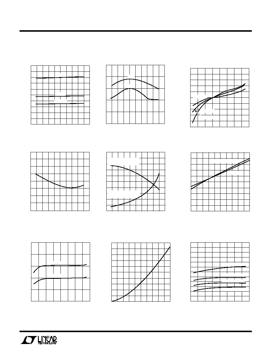
Reference Voltage
TEMPERATURE (∞C)
FLYBACK VOLTAGE (V)
25
24
23
22
21
20
19
18
17
16
15
1082 G09
≠75 ≠50
50
100
25
150 175
≠25 0
75
125
R
FB
= 3k
R
FB
= 6k
R
FB
= 10k
Supply Current vs Input Voltage**
SUPPLY VOLTAGE (V)
0
SUPPLY CURRENT (
µ
A)
200
160
120
80
40
0
30
50
80
1082 G15
10
20
40
60
70
V
C
= 50mV
V
C
= 0V
Supply Current vs Supply Voltage
(Shutdown Mode)
INPUT VOLTAGE (V)
0
SUPPLY CURRENT (mA)
20
40
60
80
1082 G14
14
13
12
11
10
9
8
7
6
5
4
3
2
10
30
50
70
90% DUTY CYCLE
50% DUTY CYCLE
10% DUTY CYCLE
0% DUTY CYCLE
**UNDER VERY LOW OUTPUT CURRENT CONDITIONS,
DUTY CYCLE FOR MOST CIRCUITS WILL APPROACH
10% OR LESS.
Feedback Bias Current vs
Temperature
TEMPERATURE (∞C)
FEEDBACK BIAS CURRENT (nA)
1082 G12
800
700
600
500
400
300
200
100
0
≠75 ≠50
50
100
25
150 175
≠25 0
75
125
Normal/Feedback Mode
Threshold on Feedback Pin
TEMPERATURE (∞C)
V
C
PIN VOLTAGE (mV)
750
725
700
675
650
625
600
575
550
525
500
1082 G16
≠75 ≠50
50
100
25
150 175
≠25 0
75
125
≠24
≠22
≠20
≠18
≠16
≠14
≠12
≠10
≠8
≠6
≠4
V
C
PIN CURRENT (
µ
A)
FEEDBACK PIN VOLTAGE
(AT THRESHOLD)
FEEDBACK PIN CURRENT
(AT THRESHOLD)
V
C
PIN VOLTAGE (mV)
SUPPLY CURRENT (
µ
A)
200
180
160
140
120
100
80
60
40
20
0
1082 G17
0
10
50
70
40
90 100
20 30
60
80
≠55∞C
T
J
125∞C
T
J
= 150∞C
Shutdown Mode Supply Current
Reference Voltage and Switching
Frequency vs Temperature
TEMPERATURE (∞C)
FREQUENCY (kHz)
70
65
60
55
50
45
1082 G11
1.250
1.245
1.240
1.235
1.230
1.225
REFERENCE VOLTAGE (V)
≠75 ≠50
50
100
25
150 175
≠25 0
75
125
FREQ
V
REF
INPUT VOLTAGE (V)
0
REFERENCE VOLTAGE CHANGE (mV)
5
4
3
2
1
0
≠1
≠2
≠3
≠4
≠5
20
40
50
1082 G10
10
30
60
70
80
T
J
= 25∞C
T
J
= ≠55∞C
T
J
= 150∞C
Line Regulation
SWITCH CURRENT (A)
DRIVER CURRENT (mA)
100
90
80
70
60
50
40
30
20
10
0
1082 G13
0
0.2
1.0
1.4
0.8
1.8 2.0
0.4 0.6
1.2
1.6
* AVERAGE SUPPLY CURRENT
= I
Q
+ DC(2.9 + 10
≠2
I
SW
+ 10
≠5
I
SW
2
)
I
Q
= QUIESCENT CURRENT, DC = DUTY CYCLE,
I
SW
= SWITCH CURRENT
Driver Current* vs Switch Current