1
LT1083/LT1084/LT1085 Fixed
DEVICE
OUTPUT CURRENT*
LT1083
7.5 Amps
LT1084
5.0 Amps
LT1085
3.0 Amps
*For a 1.5A low dropout regulator see the LT1086 data sheet.
s
Three-Terminal 3.3V, 3.6V, 5V and 12V
s
Output Current of 3A, 5A or 7.5A
s
Operates Down to 1V Dropout
s
Guaranteed Dropout Voltage at Multiple Current Levels
s
Line Regulation: 0.015%
s
Load Regulation: 0.1%
s
100% Thermal Limit Functional Test
s
Adjustable Versions Available
The LT
Æ
1083 series of positive adjustable regulators are
designed to provide 3A, 5A and 7.5A with higher efficiency
than currently available devices. All internal circuitry is
designed to operate down to 1V input to output differential
and the dropout voltage is fully specified as a function of
load current. Dropout is guaranteed at a maximum of 1.5V
at maximum output current, decreasing at lower load
currents. On-chip trimming adjusts the output voltage to
1%. Current limit is also trimmed, minimizing the stress
on both the regulator and power source circuitry under
overload conditions.
The LT1083 series devices are pin compatible with older
three-terminal regulators. A 10
µ
F output capacitor is
required on these new devices; however, this is usually
included in most regulator designs.
Unlike PNP regulators, where up to 10% of the output
current is wasted as quiescent current, the LT1083 quies-
cent current flows into the load, increasing efficiency.
3A, 5A, 7.5A Low Dropout
Positive Fixed Regulators
s
High Efficiency Linear Regulators
s
Post Regulators for Switching Supplies
s
Constant Current Regulators
s
Battery Chargers
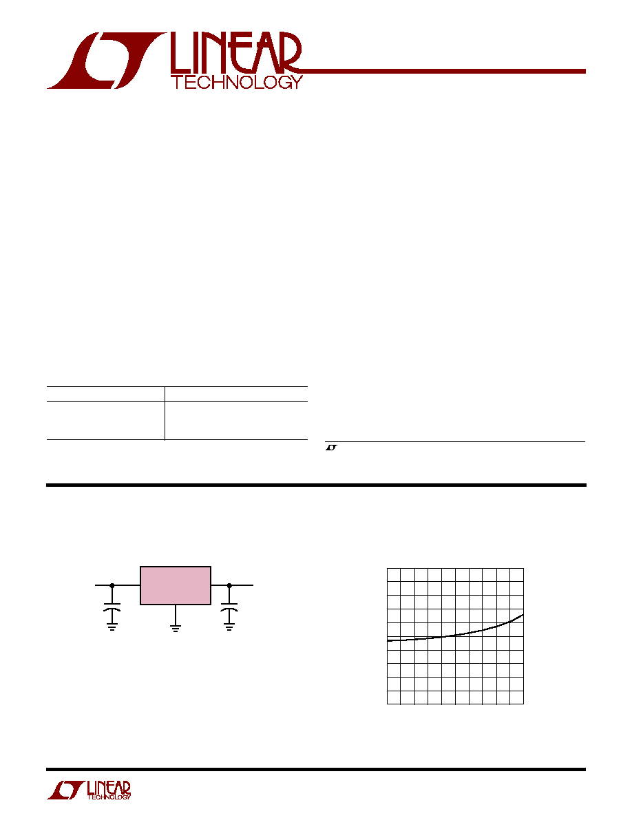
5V, 7.5A Regulator
Dropout Voltage vs Output Current
FEATURES
DESCRIPTIO
U
APPLICATIO S
U
TYPICAL APPLICATIO
U
V
IN
6.5V
5V AT 7.5A
LT1083-5
LT1083/4/5 TA01
22
µ
F*
TANTALUM
+
10
µ
F
+
*REQUIRED FOR STABILITY
OUTPUT CURRENT (A)
0
INPUT/OUTPUT VOLTAGE DIFFERENTIAL (V)
2
1
0
1083/4/5 TA02
I
FULLLOAD
/2
I
FULLLOAD
, LTC and LT are registered trademarks of Linear Technology Corporation.
2
LT1083/LT1084/LT1085 Fixed
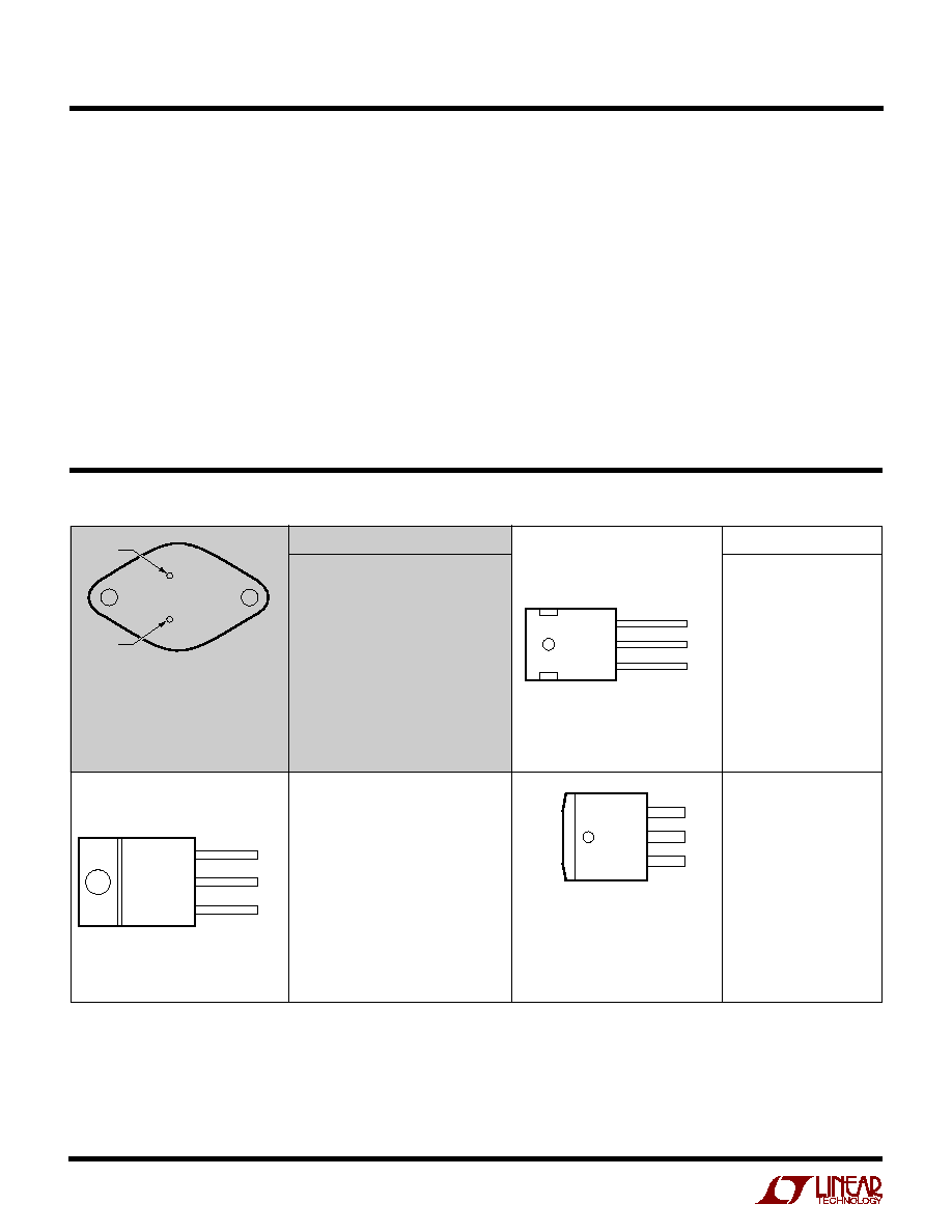
TAB IS
OUTPUT
T PACKAGE
3-LEAD PLASTIC TO-220
V
IN
V
OUT
GND
FRONT VIEW
3
2
1
Power Dissipation .............................. Internally Limited
Input Voltage* ........................................................ 30V
Operating Input Voltage
3.3V, 3.6V Devices ........................................... 20V
5V Devices ....................................................... 20V
12V Devices ..................................................... 25V
Operating Junction Temperature Range
"C" Grades
Control Section .............................. 0
∞
C to 125
∞
C
Power Transistor ............................ 0
∞
C to 150
∞
C
"M" Grades
Control Section .......................... ≠55
∞
C to 150
∞
C
Power Transistor ........................ ≠55
∞
C to 200
∞
C
Storage Temperature Range ................ ≠ 65
∞
C to 150
∞
C
Lead Temperature (Soldering, 10 sec)................. 300
∞
C
100% Thermal Limit Functional Test.
*Although the devices maximum operating voltage is limited, (20V for a
3V, 5V device, and 25V for a 12V device) the devices are guaranteed to
withstand transient input voltages up to 30V. For input voltages greater
than the maximum operating input voltage some degradation of
specifications will occur. For input/output voltage differentials greater than
15V, a minimum external load of 5mA is required to maintain regulation.
ORDER PART NUMBER
LT1083CP-5
LT1083CP-12
LT1084CP-5
LT1084CP-12
LT1083CK-5
LT1083CK-12
LT1083MK-5
LT1083MK-12
LT1084CK-5
LT1084CK-12
LT1084MK-5
LT1084MK-12
LT1085CK-5
LT1085CK-12
LT1085MK-5
LT1085MK-12
JA
= 35
∞
C/W
JA
= 45
∞
C/W
JA
= 50
∞
C/W
LT1084CT-3.3
LT1084CT-5
LT1084CT-12
LT1085CT-3.3
LT1085CT-3.6
LT1085CT-5
LT1085CT-12
LT1085CM-3.3
LT1085CM-3.6
LT1085IM-3.6
JA
= 30
∞
C/W*
*WITH PACKAGE SOLDERED TO 0.52IN
2
COPPER AREA OVER BACKSIDE GROUND
PLANE OR INTERNAL POWER PLANE.
JA
CAN
VARY FROM 20
∞
C/W TO > 40
∞
C/W DEPENDING
ON MOUNTING TECHNIQUE.
ABSOLUTE AXI U RATI GS
W
W
W
U
(Note 1)
PRECO DITIO I G
U
U
U
PACKAGE/ORDER I FOR ATIO
U
U
W
1
2
V
IN
CASE IS
OUTPUT
GND
K PACKAGE
2-LEAD TO-3 METAL CAN
V
IN
V
OUT
GND
P PACKAGE
3-LEAD TO-3P PLASTIC
FRONT VIEW
TAB IS
OUTPUT
3
2
1
ORDER PART NUMBER
TAB IS
OUTPUT
M PACKAGE
3-LEAD PLASTIC DD
FRONT VIEW
V
IN
V
OUT
GND
3
2
1
OBSOLETE NOT RECOMMENDED
FOR NEW DESIGNS
Consult factory for parts specified with wider operating temperature ranges.
3
LT1083/LT1084/LT1085 Fixed
PARAMETER
CONDITIONS
MIN
TYP
MAX
UNITS
Output Voltage
LT1084-3.3
I
OUT
= 0mA, T
J
= 25
∞
C, V
IN
= 8V (K Package Only)
3.270
3.300
3.330
V
4.8V
V
IN
15V, 0
I
OUT
I
FULLOAD
(Notes 3, 4, 9)
q
3.235
3.300
3.365
V
LT1085-3.3
V
IN
= 5V, I
OUT
= 0mA, T
J
= 25
∞
C (K Package Only)
3.270
3.300
3.330
V
4.8V
V
IN
15V, 0
I
OUT
I
FULLOAD
(Notes 3, 4, 9)
q
3.235
3.300
3.365
V
LT1085-3.6
V
IN
= 5V, I
OUT
= 0mA, T
J
= 25
∞
C (K Package Only)
3.564
3.600
3.636
V
5V
V
IN
15V, 0
I
OUT
I
FULLOAD
(Note 9)
q
3.500
3.672
V
5V
V
IN
15V, 0
I
OUT
I
FULLOAD
, TJ
0
∞
C (Notes 3, 4, 9)
3.528
3.672
V
LT1085-3.6
5V
V
IN
15V, 0
I
OUT
2.5A (Notes 3, 4, 9)
q
3.528
3.672
V
V
IN
= 4.75V, I
OUT
= 3A, T
J
0
∞
C
3.350
3.672
V
V
IN
= 4.75V, I
OUT
= 2.5A, T
J
0
∞
C
3.450
3.672
V
V
IN
= 4.75V, I
OUT
= 1.5A, T
J
> 0
∞
C
3.528
3.672
V
LT1083/4/5-5
I
OUT
= 0mA, T
J
= 25
∞
C, V
IN
= 8V (K Package Only)
4.950
5.000
5.050
V
0
I
OUT
I
FULLOAD
, 6.5V
V
IN
20V (Notes 4, 6, 7, 9)
4.900
5.000
5.100
V
LT1083/4/5-12 I
OUT
= 0mA, T
J
= 25
∞
C, V
IN
= 15V (K Package Only)
11.880
12.000
12.120
V
0
I
OUT
I
FULLOAD
, 13.5V
V
IN
25V (Notes 4, 6, 7, 9)
11.760
12.000
12.240
V
Line Regulation
LT1084-3.3
I
OUT
= 0mA, T
J
= 25
∞
C, 4.8V
V
IN
15V
0.5
6
mV
q
1.0
6
mV
LT1085-3.3
4.8V
V
IN
15V, I
OUT
= 0mA, T
J
= 25
∞
C
0.5
6
mV
q
1.0
6
mV
LT1085-3.6
4.8V
V
IN
15V, I
OUT
= 0mA, T
J
= 25
∞
C
0.5
6
mV
q
1.0
6
mV
LT1083/4/5-5
I
OUT
= 0mA, T
J
= 25
∞
C, 6.5V
V
IN
20V (Notes 2, 3)
0.5
10
mV
q
1.0
10
mV
LT1083/4/5-12 I
OUT
= 0mA, T
J
= 25
∞
C, 13.5V
V
IN
25V (Notes 2, 3)
1.0
25
mV
q
2.0
25
mV
Load Regulation
LT1084-3.3
V
IN
= 5V, 0
I
OUT
5A, T
J
= 25
∞
C
3
15
mV
q
7
20
mV
LT1085-3.3
V
IN
= 5V, 0
I
OUT
3A, T
J
= 25
∞
C
3
15
mV
q
7
20
mV
LT1085-3.6
V
IN
= 5.25V, 0
I
OUT
3A, T
J
= 25
∞
C
3
15
mV
q
7
20
mV
LT1083/4/5-5
V
IN
= 8V, 0
I
OUT
I
FULLLOAD,
T
J
= 25
∞
C (Notes 2, 3, 4, 6)
5
20
mV
q
10
35
mV
LT1083/4/5-12 V
IN
= 15V, 0
I
OUT
I
FULLLOAD,
T
J
= 25
∞
C (Notes 2, 3, 4, 6)
12
36
mV
q
24
72
mV
Dropout Voltage
LT1084/5-3.3
V
OUT
= 33mV, I
OUT
= I
FULL LOAD
(Notes 5, 6)
q
1.3
1.5
V
LT1085-3.6
V
OUT
= 36mV, I
OUT
= I
FULL LOAD
(Notes 5, 6)
q
1.3
1.5
V
LT1083/4/5-5
V
OUT
= 50mV, I
OUT
= I
FULL LOAD
(Notes 5, 6)
q
1.3
1.5
V
LT1083/4/5-12
V
OUT
= 120mV, I
OUT
= I
FULL LOAD
(Notes 5, 6)
q
1.3
1.5
V
Current Limit
LT1083-5
V
IN
= 10V
q
8.0
9.5
A
LT1083-12
V
IN
= 17V
q
8.0
9.5
A
LT1084-3.3
V
IN
= 8V
q
5.5
6.5
A
LT1084-5
V
IN
= 10V
q
5.5
6.5
A
LT1084-12
V
IN
= 17V
q
5.5
6.5
A
LT1085-3.3/3.6 V
IN
= 8V
q
3.2
4.0
A
LT1085-5
V
IN
= 10V
q
3.2
4.0
A
LT1085-12
V
IN
= 17V
q
3.2
4.0
A
ELECTRICAL CHARACTERISTICS
The
q
denotes the specifications which apply over the full operating
temperature range, otherwise specifications are at T
A
= 25
∞
C.
4
LT1083/LT1084/LT1085 Fixed
PARAMETER
CONDITIONS
MIN
TYP
MAX
UNITS
Quiescient Current
LT1084-3.3
V
IN
= 18V
q
5.0
10.0
mA
LT1085-3.3
V
IN
= 18V
q
5.0
10.0
mA
LT1085-3.6
V
IN
= 18V
q
5.0
10.0
mA
LT1083/4/5-5
V
IN
20V
q
5.0
10.0
mA
LT1083/4/5-12
V
IN
25V
q
5.0
10.0
mA
Thermal Regulation
LT1083-5/12
T
A
= 25
∞
C, 30ms pulse
0.002
0.010
%/W
LT1084-3.3/5/12
0.003
0.015
%/W
LT1085-3.3/3.6/5/12
0.004
0.020
%/W
Ripple Rejection
f = 120Hz, C
OUT
= 25
µ
F Tantalum, I
OUT
= I
FULLLOAD
(Note 4)
LT1084-3.3
f = 120Hz, C
OUT
= 25
µ
F Tantalum, I
OUT
= 5A, V
IN
= 6.3V
q
60
72
dB
LT1085-3.3
f = 120Hz, C
OUT
= 25
µ
F Tantalum, V
IN
= 6.3V, I
OUT
= 3A
q
60
72
dB
LT1085-3.6
f = 120Hz, C
OUT
= 25
µ
F Tantalum, V
IN
= 6.6V, I
OUT
= 3A
q
60
72
dB
LT1083/4/5-5
V
IN
= 8V (Note 6)
q
60
68
dB
LT1083/4/5-12
V
IN
= 15V (Note 6)
q
54
60
dB
Temperature Stability
q
0.5
%
Long Term Stability
T
A
= 125
∞
C, 1000 Hrs.
0.03
1.0
%
RMS Output Noise
T
A
= 25
∞
C,
(% of V
OUT
)
10Hz =
f
10kHz
0.003
%
Thermal Resistance
Control Circuitry/Power Transistor (See Applications Information)
Junctrion-to-Case
LT1083
K Package
0.6/1.6
∞
C/W
P Package
0.5/1.6
∞
C/W
LT1084
K Package
0.75/2.3
∞
C/W
P Package
0.65/2.3
∞
C/W
T Package
0.65/2.7
∞
C/W
LT1085
K Package
0.9/3.0
∞
C/W
T Package
0.7/3.0
∞
C/W
DD Package
0.7/3.0
∞
C/W
input to output voltage. Note that the 60W power dissipation for the
LT1083 (45W for the LT1084 (K, P), 30W for the LT1084 (T), 30W for the
LT1085) is only achievable over a limited range of input to output voltage.
Note 5: Dropout voltage is specified over the full output current range of
the device. Test points and limits are shown on the Dropout Voltage curve.
Note 6: For LT1083 I
FULL LOAD
is 5A for ≠ 55
∞
C
T
J
≠ 40
∞
C and 7.5A for
T
J
≠ 40
∞
C.
Note 7: 1.7V
(V
IN
≠ V
OUT
)
25V for LT1084 at ≠ 55
∞
C
T
J
≠ 40
∞
C.
Note 8: Dropout voltage 1.7V maximum for LT1084 at
≠ 55
∞
C
T
J
≠ 40
∞
C.
Note 9: Full load current is not available at all input-output voltages.
See Notes 3, 4, 6.
Note 1: Absolute Maximum Ratings are those values beyond which the life
of a device may be impaired.
Note 2: See thermal regulation specifications for changes in output voltage
due to heating effects. Load and line regulation are measured at a constant
junction temperature by low duty cycle pulse testing.
Note 3: Line and load regulation are guaranteed up to the maximum power
dissipation (60W for the LT1083, 45W for the LT1084 (K, P), 30W for the
LT1084 (T) and 30W for the LT1085). Power dissipation is determined by
the input/output differential and the output current. Guaranteed maximum
power dissipation will not be available over the full input/output range.
Note 4: I
FULL LOAD
is defined in the current limit curves. The I
FULLLOAD
curve is defined as the minimum value of current limit as a function of
ELECTRICAL CHARACTERISTICS
The
q
denotes the specifications which apply over the full operating
temperature range, otherwise specifications are at T
A
= 25
∞
C.
5
LT1083/LT1084/LT1085 Fixed
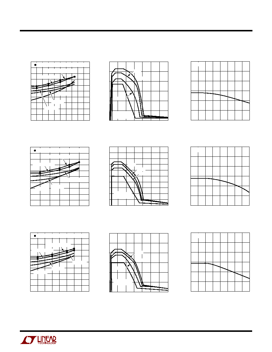
LT1084 Dropout Voltage
LT1084 Short Circuit Current
LT1084 Load Regulation
OUTPUT CURRENT (A)
0
0
MINIMUN INPUT/OUTPUT DIFFERENTIAL (V)
1
1
2
3
4
LT1083/4/5 FIXEDG04
5
2
6
INDICATES GUARANTEED TEST POINT
≠55
∞
C
T
J
150
∞
C
0
∞
C
T
J
125
∞
C
T
J
= 150
∞
C
T
J
= ≠55
∞
C
T
J
= 25
∞
C
INPUT/OUTPUT DIFFERENTIAL (V)
0
0
SHORT-CIRCUIT CURRENT (A)
1
3
4
5
10
7
10
20
25
LT1083/4/5 FIXED G05
2
8
9
6
5
15
30
35
25
∞
C
≠55
∞
C
150
∞
C
GUARANTEED
I
FULL LOAD
TEMPERATURE (
∞
C)
≠50
≠0.20
≠0.15
≠0.10
≠0.05
0.05
0.10
OUTPUT VOLTAGE DEVIATION (%)
0
0
50
100
150
LT1083/4/5 FIXED G06
≠25
25
75
125
I = 5A
LT1085 Dropout Voltage
OUTPUT CURRENT (A)
0
0
MINIMUM INPUT/OUTPUT DIFFERENTIAL (V)
1
2
1
2
LT1083/4/5 FIXED G07
3
4
INDICATES GUARANTEED TEST POINT
T
J
= 150
∞
C
T
J
= 25
∞
C
≠55
∞
C
T
J
150
∞
C
T
J
= ≠55
∞
C
0
∞
C
T
J
125
∞
C
TEMPERATURE (
∞
C)
≠50
≠0.20
≠0.15
≠0.10
≠0.05
0.05
0.10
OUTPUT VOLTAGE DEVIATION (%)
0
0
50
100
150
LT1083/4/5 FIXED G09
≠25
25
75
125
I = 3A
LT1085 Load Regulation
INPUT/OUTPUT DIFFERENTIAL (V)
0
SHORT-CIRCUIT CURRENT (A)
4
5
6
15
25
LT1083/4/5 FIXED G08
3
2
5
10
20
30
35
1
0
25
∞
C
≠55
∞
C
I
FULL LOAD
GUARANTEED
150
∞
C
LT1085 Short-Circuit Current
OUTPUT CURRENT (A)
0
MINIMUM INPUT/OUTPUT DIFFERENTIAL (V)
1
2
LT1083/4/5 FIXED G01
0
1
2
3
4
5
6
7
8
9
10
INDICATES GUARANTEED TEST POINT
≠40
∞
C
T
J
150
∞
C
0
∞
C
T
J
125
∞
C
T
J
= 150
∞
C
T
J
= 25
∞
C
T
J
= ≠55
∞
C
INPUT/OUTPUT DIFFERENTIAL (V)
0
SHORT-CIRCUIT CURRENT (A)
8
10
12
15
25
LT1083/4/5 FIXED G02
6
4
5
10
20
30
35
2
0
25
∞
C
150
∞
C
I
FULL LOAD
GUARANTEED
≠55
∞
C
TEMPERATURE (
∞
C)
≠50
≠0.20
OUTPUT VOLTAGE DEVIATION (%) ≠0.15
≠0.10
≠0.05
0
0
50
100
150
LT1083/4/5 FIXED G03
0.05
0.10
≠25
25
75
125
I = 7.5A
LT1083 Dropout Voltage
LT1083 Load Regulation
LT1083 Short-Circuit Current
TYPICAL PERFOR A CE CHARACTERISTICS
U
W