 | –≠–ª–µ–∫—Ç—Ä–æ–Ω–Ω—ã–π –∫–æ–º–ø–æ–Ω–µ–Ω—Ç: LT1089 | –°–∫–∞—á–∞—Ç—å:  PDF PDF  ZIP ZIP |

LT1089
1
1089fa
7.5A Switch Capability
Low Series Drop (< 1.5V at 7.5A)
Logic Input (Positive or Negative Logic)
Current Limited
Thermal Overload
5mA Quiescent Current
10µs Risetime
The LT
Æ
1089 is a logic driven, high current, high side
switch utilizing bipolar technology. The device is capable
of driving loads up to 7.5A with a low series drop of only
1.5V, and the series drop is specified over the full range of
switch currents. The device has internal current limiting
and thermal overload protection. The input logic is
designed so that the output can drive loads referenced
either above or below the device ground pin. Either
positive or negative logic can be used to drive the input.
The device is available in both TO-3 metal can and TO-220
plastic packages.
High Side Switch
, LTC and LT are registered trademarks of Linear Technology Corporation.
FEATURES
DESCRIPTIO
U
LT1089 Switch Voltage
vs Output Current
LT1089 ∑ BD01
V
OUT
V
CC
I
Q
5mA
LOGIC IN
LOGIC GND
BIAS,
THERMAL LIMIT,
CURRENT LIMIT,
OUTPUT DRIVE
SWITCH CURRENT (A)
0
SWITCH FORWARD DROP (V)
2
1
8
0
2
1
4
3
6
7
9
5
10
LT1089 ∑ BD02
INDICATES GUARANTEED TEST POINT
T
J
= ≠ 55∞C
T
J
= 25∞C
T
J
= 150∞C
0∞C T
J
125∞C
≠ 55∞C T
J
150∞C
BLOCK DIAGRA
W
LT1089
2
1089fa
Switch Voltage (V
CC
≠ V
OUT
) .................................. 30V
Logic Input Voltage (V
IN
≠ GND) ............................ 15V
Logic Input Voltage Range (V
lN
) .. (V
CC
≠ 30V) < V
IN
< V
CC
Ground Pin Voltage Range (GND) .. (V
CC
≠ 30V) < GND < V
CC
Operating Junction Temperature Range
LT1089M Grades ................................ ≠ 55∞C to 150∞C
LT1089C Grades ...................................... 0∞C to 125∞C
Storage Temperature Range ................. ≠ 65∞C to 150∞C
Lead Temperature (Soldering, 10 sec).................. 300∞C
Consult LTC Marketing for parts specified with wider operating temperature
ranges.
(Note 1)
ABSOLUTE AXI U RATI GS
W
W
W
U
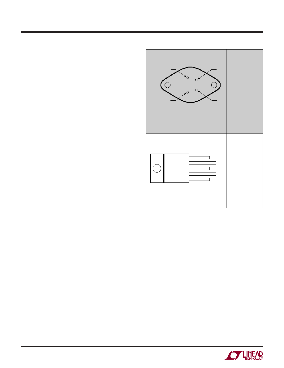
PACKAGE/ORDER I FOR ATIO
U
U
W
Switch Voltage (V
CC
≠ V
OUT
) ................................. 20V
Logic Input Voltage (V
IN
≠ GND) .............................. 5V
Logic Input Voltage Range (V
lN
) ...... (V
CC
≠ 20V) < V
IN
< V
CC
Ground Pin Voltage Range (GND)....(V
CC
≠ 20V) < GND < V
CC
*Maximum operating specifications are the maximum recommended
operating voltages. The device is fully specified up to the maximum
operating specifications. For voltages greater than the maximum
operating specifications some device parameters may exceed the data
sheet limits.
AXI U OPERATI
N
G
SPECIFICATIO
N
S*
W
W
W
U
U
2
4
1
3
V
IN
NC
GND
CASE IS
V
OUT
LOGIC IN
K PACKAGE
4-LEAD TO-3 METAL CAN
BOTTOM VIEW
ORDER PART
NUMBER
LT1089MK
LT1089CK
ORDER PART
NUMBER
LT1089 ∑ POI01
LT1089CT
T PACKAGE
5-LEAD TO-220
FRONT VIEW
LOGIC IN
V
IN
V
OUT
GND
NC
5
4
3
2
1
OBSOLETE PACKAGE
Consider the T Package as an Alternate Source

LT1089
3
1089fa
PARAMETER
CONDITIONS (NOTE 2)
MIN
TYP
MAX
UNITS
Output Saturation Voltage
I
SWITCH
= 7.5A, (V
IN
≠ GND) = 5V,
1.3
1.5
V
4V (V
CC
≠ GND) < 20V
Input Voltage (V
IN
≠ GND)
Switch ON,
1.5
V
(Note 3) 4V < (V
CC
≠ GND) < 20V
2.4
V
Switch OFF,
1.5
V
(Note 4) 4V < (V
CC
≠ GND) < 20V
0.8
V
Input Current
Switch ON, (V
IN
≠ GND) = 5V
≠ 20
µA
≠ 100
µA
Switch OFF, (V
IN
≠ GND) = 0V
0
µA
±5
µA
Ground Pin Current
Switch ON, (V
IN
≠ GND) = 5V
3.5
m A
5.0
m A
Switch OFF, (V
IN
≠ GND) = 0V
0
µA
±20
µA
Output Current
Switch OFF, (V
IN
≠ GND) = 0V
5
10
mA
Current Limit
Switch ON, (V
IN
≠ GND) = 5V
(V
CC
≠ V
OUT
) = 5V
8.0
9.5
12.0
A
(V
CC
≠ V
OUT
) = 20V
0.5
1.0
1.5
A
Turn-On Delay
1
µs
10
µs
Turn-Off Delay
5
µs
20
µs
Output Risetime
R
LOAD
= 4
10
µs
25
µs
Output Falltime
R
LOAD
=
4 (Note 5)
10
µs
25
µs
Thermal Resistance
K Package
1.6
∞C/ W
T Package
2.0
∞C/ W
ELECTRICAL CHARACTERISTICS
The
denotes the specifications which apply over full operating
temperature range. (Note 1)
Note 1: Absolute Maximum Ratings are those values beyond which the life
of a device may be impaired.
Note 2: Unless otherwise specified, (V
CC
≠ GND) = 20V and the output
load is referred to the ground pin (GND) of the device. Positive current
values are defined to flow out of the device.
Note 3: For input voltages greater than 2.4V the device Is guaranteed to be
turned on. 1.5V is the typical threshold at 25∞C.
Note 4: For input voltages less than 0.8V, the device is guaranteed to be in
an off state. 1.5V is the typical switch threshold at 25∞C.
Note 5: For reactive loads such as large capacitors, the output falltime will
be determined by the load.
LT1089
4
1089fa
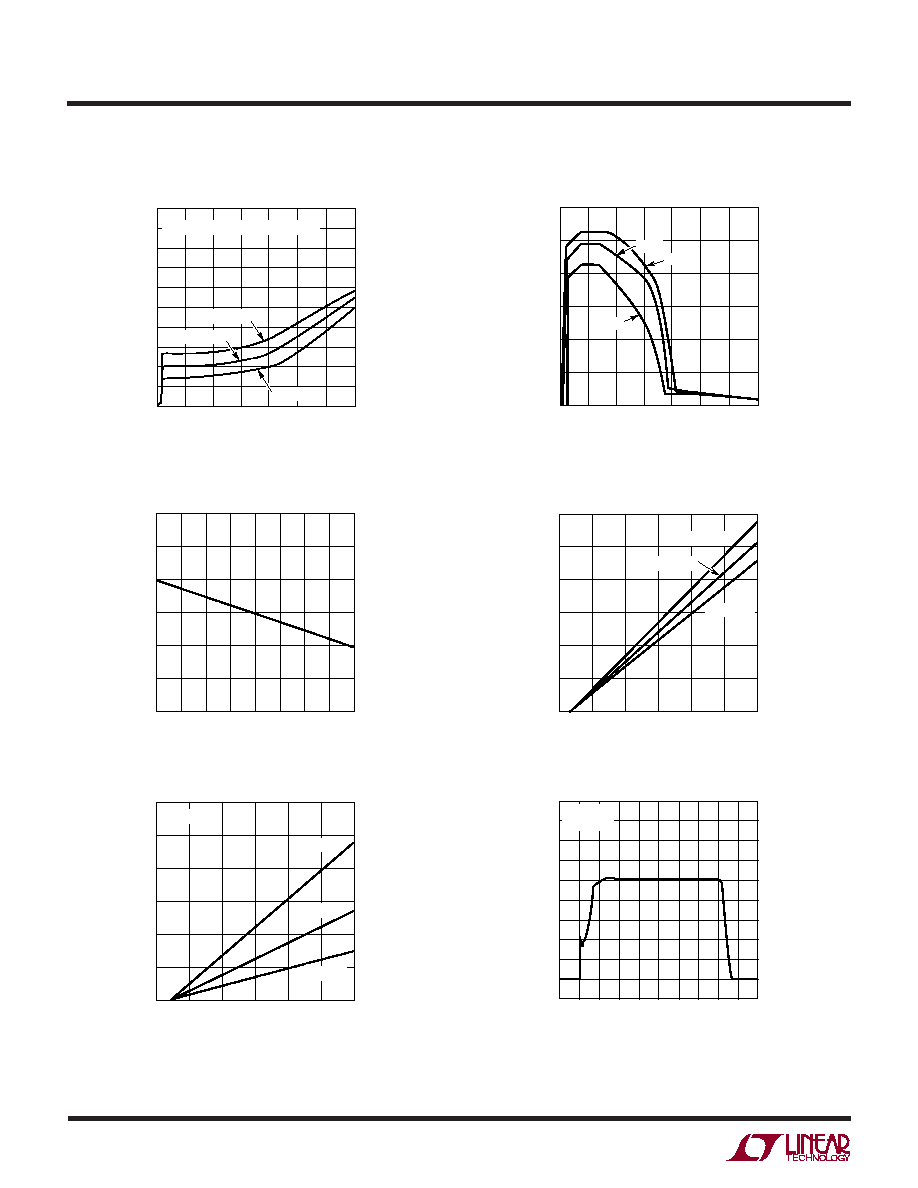
TYPICAL PERFOR A CE CHARACTERISTICS
U
W
Minimum Output Current
Short-Circuit Current
SWITCH VOLTAGE (V)
0
0
MINIMUM OUTPUT CURRENT (mA)
1
3
4
5
10
7
10
20
25
LTC1089 ∑ TPC01
2
8
9
6
5
15
30
35
(LOGIC IN ≠ GND) = 0V SWITCH OFF
T
J
= 150∞C
T
J
= ≠ 55∞C
T
J
= 25∞C
LTC1089 ∑ TPC02
SWITCH VOLTAGE (V
CC
≠ V
OUT
) (V)
0
SHORT-CIRCUIT CURRENT (A)
8
10
12
15
25
6
4
5
10
20
30
35
2
0
≠55∞C
150∞C
25∞C
Input Trip Voltage
(Logic In ≠ GND)
LTC1089 ∑ TPC03
JUNCTION TEMPERATURE (∞C)
≠ 50
0
INPUT TRIP POINT (V)
0.5
1.0
1.5
2.0
0
50
100
150
2.5
3.0
≠ 25
25
75
125
Rise and Fall Times
Logic Input Current
Ground Pin Current
LTC1089 ∑ TPC04
INPUT VOLTAGE (LOGIC IN ≠ GND) (V)
0
0
GROUND PIN CURRENT (mA)
5
10
15
5
10
15
T
J
= 125∞C
T
J
= ≠55∞C
T
J
= 25∞C
LTC1089 ∑ TPC05
INPUT VOLTAGE (LOGIC IN ≠ GND) (V)
0
0
INPUT CURRENT (
µ
A)
50
100
150
5
10
15
T
J
= 125∞C
T
J
= ≠ 55∞C
V
CC
= 20V
T
J
= 25∞C
LTC1089 ∑ TPC06
TIME (µs)
0
OUTPUT VOLTAGE (V)
10
14
18
80
6
2
8
12
16
4
0
≠2
20
10
40
30
60 70
90
50
100
R
L
= 2
V
OUT
= 10V
LT1089
5
1089fa
Driving Ground Referred Loads
Driving Negative Referred Loads
Driving Inductive Loads
LT1089 ∑ TA01
V
OUT
12V
LOGIC
IN
LT1089
LT1089 ∑ TA02
V
OUT
12V
≠5V
LOGIC
IN
LT1089
LT1089 ∑ TA03
V
OUT
12V
20V
LOGIC
IN
LT1089
TYPICAL APPLICATIO S
U
APPLICATIO HI TS
U
U
The logic and ground pins function as a differential logic
input with a common-mode range of V
CC
to V
CC
≠ 20V and
a differential threshold voltage (V
LOGIC
≠ GND) of 1.5V.
Note that if either Logic In or GND are left open the switch
remains inactive.
The LT1089 must be protected against overvoltage at
turn-off when driving inductive loads. The inductive flyback
voltage can easily exceed the maximum operating switch
voltage (V
CC
≠ V
OUT
) of 20V, potentially damaging the
switch. The solution is to clamp the switch voltage to 20V
or less with a zener diode. Remember that the switch can
handle 7.5A and the Zener may be required to handle the
same amount of current.
Care must be exercised when operating near the
maximum switch voltage. A high current or capacitive load
may trip the current limit circuit at turn-on, thereby
adversely affecting the risetime of V
OUT
. The risetime is
then governed by the current limit divided by the load
capacitance, while the falltime is a function of the complex
load. In addition, at switch voltages greater than 18V
the switch current must be less than 0.5A or the device
output will not pull up. Check the short circuit current
characteristics for more detailed information.

LT1089
6
1089fa
U
PACKAGE DESCRIPTIO
K Package
4-Lead TO-3 Metal Can
(Reference LTC DWG # 05-08-1311)
OBSOLETE PACKAGE
K4(TO-3) 1098
72∞
18∞
0.490 ≠ 0.510
(12.45 ≠ 12.95)
R
0.470 TP
P.C.D.
0.167 ≠ 0.177
(4.24 ≠ 4.49)
R
0.151 ≠ 0.161
(3.84 ≠ 4.09)
DIA 2 PLC
0.655 ≠ 0.675
(16.64 ≠ 19.05)
1.177 ≠ 1.197
(29.90 ≠ 30.40)
0.038 ≠ 0.043
(0.965 ≠ 1.09)
0.060 ≠ 0.135
(1.524 ≠ 3.429)
0.320 ≠ 0.350
(8.13 ≠ 8.89)
0.420 ≠ 0.480
(10.67 ≠ 12.19)
0.760 ≠ 0.775
(19.30 ≠ 19.69)

LT1089
7
1089fa
Information furnished by Linear Technology Corporation is believed to be accurate and reliable.
However, no responsibility is assumed for its use. Linear Technology Corporation makes no represen-
tation that the interconnection of its circuits as described herein will not infringe on existing patent rights.
U
PACKAGE DESCRIPTIO
T Package
5-Lead Plastic TO-220 (Standard)
(Reference LTC DWG # 05-08-1421)
T5 (TO-220) 0801
.028 ≠ .038
(0.711 ≠ 0.965)
.067
(1.70)
.135 ≠ .165
(3.429 ≠ 4.191)
.700 ≠ .728
(17.78 ≠ 18.491)
.045 ≠ .055
(1.143 ≠ 1.397)
.095 ≠ .115
(2.413 ≠ 2.921)
.013 ≠ .023
(0.330 ≠ 0.584)
.620
(15.75)
TYP
.155 ≠ .195*
(3.937 ≠ 4.953)
.152 ≠ .202
(3.861 ≠ 5.131)
.260 ≠ .320
(6.60 ≠ 8.13)
.165 ≠ .180
(4.191 ≠ 4.572)
.147 ≠ .155
(3.734 ≠ 3.937)
DIA
.390 ≠ .415
(9.906 ≠ 10.541)
.330 ≠ .370
(8.382 ≠ 9.398)
.460 ≠ .500
(11.684 ≠ 12.700)
.570 ≠ .620
(14.478 ≠ 15.748)
.230 ≠ .270
(5.842 ≠ 6.858)
BSC
SEATING PLANE
* MEASURED AT THE SEATING PLANE
LT1089
8
1089fa
Linear Technology Corporation
1630 McCarthy Blvd., Milpitas, CA 95035-7417
(408) 432-1900
FAX: (408) 434-0507
www.linear.com
LW/TP 1002 1K REV A ∑ PRINTED IN USA
LINEAR TECHNOLOGY CORPORATION 1989
PART NUMBER
DESCRIPTION
COMMENTS
LTC1155
Dual High Side Micropower MOSFET Driver
No External Charge Pump Required; N-Channel MOSFET
LT1160/LT1162
Half/Full-Bridge N-Channel MOSFET Drivers
60V Floating Switch; Prevent Shoot Through
LTC1693
High Speed Single/Dual N-Channel MOSFET Drivers
SO-8; 1.5A Peak Output Current
LTC1693-5
High Speed Single P-Channel MOSFET Driver
16ns Rise/Fall Times at V
CC
= 12V, C
L
= InF
LTC1710
SMBus Dual High Side Switch
Two 0.4/300mA N-Channel Switches
LTC1981/LTC1982
Single and Dual Micropower High Side Switch Controllers in SOT-23
No External Components Required
LTC4412
Low Loss PowerPath Controller
Automatic Switching Between DC Sources
RELATED PARTS