 | –≠–ª–µ–∫—Ç—Ä–æ–Ω–Ω—ã–π –∫–æ–º–ø–æ–Ω–µ–Ω—Ç: LT1097S8 | –°–∫–∞—á–∞—Ç—å:  PDF PDF  ZIP ZIP |

1
LT1097
Low Cost, Low Power
Precision Op Amp
FEATURES
DESCRIPTIO
N
U
s
Offset Voltage
50
µ
V Max
s
Offset Voltage Drift
1
µ
V/
∞
C Max
s
Bias Current
250pA Max
s
Offset Current
250pA Max
s
Bias and Offset Current Drift
4pA/
∞
C Max
s
Supply Current
560
µ
A Max
s
0.1Hz to 10Hz Noise
0.5
µ
Vp-p, 2.2pAp-p
s
CMRR
115dB Min
s
Voltage Gain
117dB Min
s
PSRR
114dB Min
s
Guaranteed Operation on Two NiCad Batteries
APPLICATIO
N
S
U
s
Replaces OP-07/OP-77/OP-97/OP-177/AD707/
LT1001 with Improved Price/Performance
s
High Impedance Difference Amplifiers
s
Logarithmic Amplifiers (Wide Dynamic Range)
s
Thermocouple Amplifiers
s
Precision Instrumentation
s
Active Filters (with Small Capacitors)
TYPICAL APPLICATIO
N
U
, LTC and LT are registered trademarks of Linear Technology Corporation.
LT
Æ
1097 achieves a new standard in combining low price
and outstanding precision performance.
On all operational amplifier data sheets, the specifications
listed on the front page are for highly selected, expensive
grades, while the specs for the low cost grades are buried
deep in the data sheet.
The LT1097 does not have any selected grades, the
outstanding specifications shown in the Features section
are for its only grade.
The design effort of the LT1097 concentrated on optimiz-
ing the performance of all precision specs--at only 350
µ
A
of supply current. Typical values are 10
µ
V offset voltage,
40pA bias and offset currents, 0.2
µ
V/
∞
C and 0.4pA/
∞
C
drift. Common mode and power supply rejections, voltage
gain are typically in excess of 128dB.
All parameters that are important for precision, low power
op amps have been optimized. Consequently, using the
LT1097 error budget calculations in most applications is
unnecessary.
+
9V
OUT = 1.1V TO 8.0V
AS 1.8k
R2
135k
LT1097∑TA01
4
2
3
7
6
R1
20k
R2
1.018235V
2N3609
SATURATED
STANDARD
CELL #101
EPPLEY LABS
NEWPORT, R. I.
THE TYPICAL 40pA BIAS CURRENT OF THE LT1097
WILL DEGRADE THE STANDARD CELL BY ONLY
1ppm/YEAR. NOISE IS A FRACTION OF A ppm.
UNPROTECTED GATE MOSFET ISOLATES
STANDARD CELL ON POWER DOWN.
≠
+
LT1097
INPUT OFFSET VOLTAGE (
µ
V)
≠50 ≠40 ≠30 ≠20 ≠10 0
10 20 30 40 50
PERCENT OF UNITS
LT1097 ∑ G01
50
40
30
20
10
0
V
S
=
±
15V
T
A
= 25
∞
C
6,500 UNITS IN SO PACKAGE
6,680 UNITS IN
PLASTIC
DIP
13,180 UNITS
TESTED
Input Offset Voltage Distribution
Saturated Standard Cell Amplifier
2
LT1097
ABSOLUTE
M
AXI
M
U
M
RATINGS
W
W
W
U
PACKAGE/ORDER I
N
FOR
M
ATIO
N
W
U
U
ORDER
PART NUMBER
LT1097CN8
Supply Voltage ......................................................
±
20V
Differential Input Current (Note 1) ......................
±
10mA
Input Voltage .........................................................
±
20V
Output Short Circuit Duration .......................... Indefinite
1
2
3
4
8
7
6
5
TOP VIEW
V
OS
TRIM
≠IN
+IN
V
≠
V
OS
TRIM
V
+
OUT
OVER COMP
N8 PACKAGE
8-LEAD PLASTIC DIP
1
2
3
4
8
7
6
5
TOP VIEW
S8 PACKAGE
8-LEAD PLASTIC SO
V
OS
TRIM
≠IN
+IN
V
≠
V
OS
TRIM
V
+
OUT
OVER COMP
ORDER
PART NUMBER
LT1097S8
ELECTRICAL CHARACTERISTICS
V
S
=
±
15V, V
CM
= 0V, T
A
= 25
∞
C, unless otherwise noted.
LT1097CN8
LT1097S8
SYMBOL
PARAMETER
CONDITIONS
MIN
TYP
MAX
MIN
TYP
MAX
UNITS
V
OS
Input Offset Voltage
10
50
10
60
µ
V
V
OS
Long Term Input Offset
0.3
0.3
µ
V/Mo
TIME
Voltage Stability
I
OS
Input Offset Current
40
250
60
350
pA
I
B
Input Bias Current
±
40
±
250
±
50
±
350
pA
e
n
Input Noise Voltage
0.1Hz to 10Hz
0.5
0.5
µ
Vp-p
Input Noise Voltage Density
f
O
= 10Hz
16
16
nV/
Hz
f
O
= 1000Hz
14
14
nV/
Hz
i
n
Input Noise Current
0.1Hz to 10Hz
2.2
2.4
pAp-p
Input Noise Current Density
f
O
= 10Hz
0.03
0.035
pA/
Hz
f
O
= 1000Hz
0.008
0.008
pA/
Hz
Input Resistance
(Note 2)
Differential Mode
30
80
25
70
M
Common Mode
10
12
8∑10
11
Input Voltage Range
±
13.5
±
14.3
±
13.5
±
14.3
V
CMRR
Common Mode Rejection Ratio
V
CM
=
±
13.5V
115
130
115
130
dB
PSRR
Power Supply Rejection Ratio
V
S
=
±
1.2V to
±
20V
114
130
114
130
dB
A
VOL
Large Signal Voltage Gain
V
O
=
±
12V, R
L
= 10k
700
2500
700
2500
V/mV
V
O
=
±
10V, R
L
= 2k
250
1000
250
1000
V/mV
V
OUT
Output Voltage Swing
R
L
= 10k
±
13
±
13.8
±
13
±
13.8
V
R
L
= 2k
±
11.5
±
13
±
11.5
±
13
V
SR
Slew Rate
0.1
0.2
0.1
0.2
V/
µ
s
GBW
Gain Bandwidth Product
700
700
kHz
I
S
Supply Current
350
560
350
560
µ
A
Offset Adjustment Range
R
POT
= 10k, Wiper to V
+
±
600
±
600
µ
V
Minimum Supply Voltage
(Note 3)
±
1.2
--
±
1.2
--
V
Operating Temperature Range .................≠40
∞
C to 85
∞
C
Storage Temperature Range ..................≠65
∞
C to 150
∞
C
Lead Temperature (Soldering, 10 sec).................. 300
∞
C
3
LT1097
ELECTRICAL CHARACTERISTICS
V
S
=
±
15V, V
CM
= 0V, 0
∞
C
T
A
70
∞
C, unless otherwise noted.
LT1097CN8
LT1097S8
SYMBOL
PARAMETER
CONDITIONS
MIN
TYP
MAX
MIN
TYP
MAX
UNITS
V
OS
Input Offset Voltage
q
20
100
20
130
µ
V
Average Temperature Coefficient of (Note 4)
q
0.2
1
0.2
1.4
µ
V/
∞
C
Input Offset Voltage
I
OS
Input Offset Current
q
60
430
75
570
pA
Average Temperature Coefficient of (Note 4)
q
0.4
4
0.5
5
pA/
∞
C
Input Offset Current
I
B
Input Bias Current
q
±
60
±
430
±
75
±
570
pA
Average Temperature Coefficient of (Note 4)
q
0.4
4
0.5
5
pA/
∞
C
Input Bias Current
A
VOL
Large Signal Voltage Gain
V
OUT
=
±
12V, R
L
10k
q
450
2000
450
2000
V/mV
V
OUT
=
±
10V, R
L
2k
q
180
800
180
800
V/mV
CMRR
Common Mode Rejection Ratio
V
CM
=
±
13.5V
q
112
128
112
128
dB
PSRR
Power Supply Rejection Ratio
V
S
=
±
1.3V to
±
20V
q
111
128
111
128
dB
Input Voltage Range
q
±
13.5
±
14.2
±
13.5
±
14.2
V
V
OUT
Output Voltage Swing
R
L
= 10k
q
±
13
±
13.7
±
13
±
13.7
V
I
S
Supply Current
q
380
700
380
700
µ
A
ELECTRICAL CHARACTERISTICS
V
S
=
±
15V, V
CM
= 0V, ≠40
∞
C
T
A
85
∞
C, unless otherwise noted. (Note 5)
LT1097CN8
LT1097S8
SYMBOL
PARAMETER
CONDITIONS
MIN
TYP
MAX
MIN
TYP
MAX
UNITS
V
OS
Input Offset Voltage
q
25
130
30
170
µ
V
Average Temperature Coefficient of
q
0.3
1.2
0.3
1.6
µ
V/
∞
C
Input Offset Voltage
I
OS
Input Offset Current
q
70
600
85
750
pA
Average Temperature Coefficient of
q
0.5
5
0.6
6
pA/
∞
C
Input Offset Current
I
B
Input Bias Current
q
±
70
±
600
±
85
±
750
pA
Average Temperature Coefficient of
q
0.5
5
0.6
6
pA/
∞
C
Input Bias Current
A
VOL
Large Signal Voltage Gain
V
OUT
=
±
12V, R
L
10k
q
300
1700
300
1700
V/mV
V
OUT
=
±
10V, R
L
2k
q
700
700
V/mV
CMRR
Common Mode Rejection Ratio
V
CM
=
±
13.5V
q
108
127
108
127
dB
PSRR
Power Supply Rejection Ratio
V
S
=
±
1.5V to
±
20V
q
108
127
108
127
dB
Input Voltage Range
q
±
13.5
±
14
±
13.5
±
14
V
V
OUT
Output Voltage Swing
R
L
= 10k
q
±
13
±
13.6
±
13
±
13.6
V
I
S
Supply Current
q
400
800
400
800
µ
A
The
q
denotes specifications which apply over the full operating
temperature range.
Note 1: Differential input voltages greater than 1V will cause excessive
current to flow through the input protection diodes unless limiting
resistance is used.
Note 2: This parameter is guaranteed by design and is not tested.
Note 3: Power supply rejection ratio is measured at the minimum supply
voltage.
Note 4: This parameter is not 100% tested.
Note 5: The LT1097 is designed, characterized and expected to meet these
extended temperature limits, but is not tested at ≠40
∞
C and 85
∞
C.
Guaranteed I grade parts are available; consult factory.
4
LT1097
TYPICAL PERFOR
M
A
N
CE CHARACTERISTICS
U
W
Distribution to Offset Voltage Drift
with Temperature
Input Bias Current vs Temperature
Minimum Supply Voltage,
Common Mode Range and
Voltage Swing at V
MIN
Warm-Up Drift
Input Bias Current Over Common
Mode Range
OFFSET VOLTAGE DRIFT WITH TEMPERATURE (
µ
V/
∞
C)
≠1.5 ≠1.2 ≠0.9 ≠0.6 ≠0.3 0
0.3 0.6 0.9 1.2 1.5
PERCENT OF UNITS
LT1097 ∑ G02
50
40
30
20
10
0
V
S
=
±
15V
240 UNITS TESTED
IN N8 PACKAGES
FROM SIX RUNS
TIME AFTER POWER ON (MINUTES)
0
1
2
3
4
5
CHANGE IN OFFSET VOLTAGE (
µ
V)
1097 ∑ G05
5
4
3
2
1
0
V
S
=
±
15V
T
A
= 25
∞
C
PLASTIC-IN-LINE PACKAGE
PLASTIC (N) OR SO (S)
TEMPERATURE (
∞
C)
≠50
0
50
≠25
25
75
100
INPUT BIAS CURRENT (pA)
1097 ∑ G03
200
100
0
≠100
≠200
≠300
UNDERCANCELLED UNIT
OVERCANCELLED UNIT
TEMPERATURE (
∞
C)
≠40
≠10
20
50
80
110
COMMON MODE RANGE OR OUTPUT SWING (V)
1097 ∑ G04
MINIMUM SUPPLY VOLTAGE, V
MIN
(V)
V
+
V
+
≠0.2
V
+
≠0.4
V
+
≠0.6
V
+
≠0.8
V
≠
+0.8
V
≠
+0.6
V
≠
+0.4
V
≠
+0.2
V
≠
±
1.4
±
1.2
±
1.0
±
0.8
CM RANGE
CM RANGE
SWING
R
L
= 10k
SWING
COMMON MODE INPUT VOLTAGE
≠15
≠5
5
≠10
0
10
15
INPUT BIAS CURRENT (pA)
1097 ∑ G06
120
80
40
0
≠40
≠80
≠120
V
S
=
±
15V
T
A
= 25
∞
C
R
IN CM
= 10
12
DEVICE WITH POSITIVE INPUT CURRENT
DEVICE WITH NEGATIVE INPUT CURRENT
V
CM
I
B
+
≠
5
LT1097
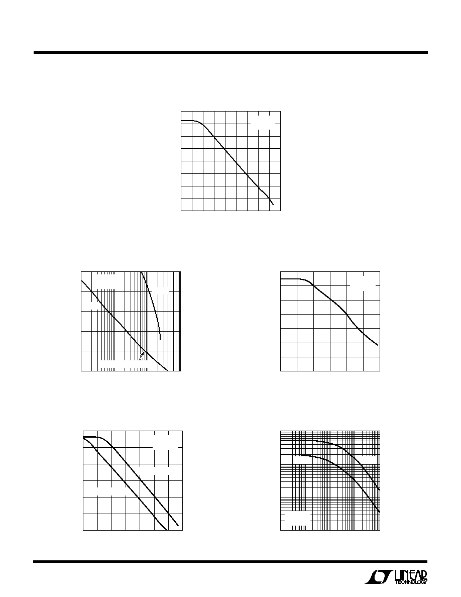
Output Short Circuit Current vs Time
TYPICAL PERFOR
M
A
N
CE CHARACTERISTICS
U
W
0.1Hz to 10Hz Noise
0.01Hz to 10Hz Noise
Noise Spectrum
TIME (SECONDS)
0
2
4
6
8
10
NOISE VOLTAGE (0.4
µ
V/DIV)
1097 ∑ G08
V
S
=
±
1.2V TO
±
20V
T
A
= 25
∞
C
TIME FROM OUTPUT SHORT (MINUTES)
0
1
2
3
SHORT CIRCUIT CURRENT (mA)
SINKING
SOURCING
1097 ∑ G07
20
15
10
5
0
≠5
≠10
≠15
≠20
V
S
=
±
15V
T
A
= 25
∞
C
TIME (SECONDS)
0
20
40
60
80
100
NOISE VOLTAGE (0.4
µ
V/DIV)
0.4
µ
V
1097 ∑ G09
V
S
=
±
1.2V TO
±
20V
T
A
= 25
∞
C
FREQUENCY (Hz)
1
1
10
100
1000
10
100
1000
1097 ∑ G10
VOLTAGE NOISE DENSITY (nV
Hz)
CURRENT NOISE DENSITY (fA
Hz)
T
A
= 25
∞
C
V
S
=
±
1.2V TO
±
20V
VOLTAGE NOISE
1/f CORNER
2.5Hz
1/f CORNER
140Hz
CURRENT NOISE
OUTPUT VOLTAGE (V)
≠15
≠5
5
≠10
0
10
15
CHANGE IN OFFSET VOLTAGE (
µ
V)
1097 ∑ G11
≠30
≠20
≠10
0
10
20
30
V
s
=
±
15 V
T
A
= 25
∞
C
R
L
= 10k
R
L
= 10k
R
L
= 2k
R
L
= 2k
Voltage Gain
6
LT1097
FREQUENCY (Hz)
0.01 0.1
1
10 100 1k 10k 100k 1M 10M
VOLTAGE GAIN (dB)
1097 ∑ G12
140
120
100
80
60
40
20
0
≠20
V
S
=
±
15V
T
A
= 25
∞
C
FREQUENCY (MHz)
0.01
GAIN (dB)
40
30
20
10
0
≠10
PHASE SHIFT (DEGREES)
100
120
140
160
180
200
0.1
1
10
1097 ∑ G13
V
S
=
±
15V
T
A
= 25
∞
C
PHASE
GAIN
PHASE MARGIN = 70
∞
C
FREQUENCY (Hz)
1
10
100
1k
10k
100k
1M
COMMON MODE REJCTION RATIO (dB)
1097 ∑ G14
140
120
100
80
60
40
20
0
V
S
=
±
15V
T
A
= 25
∞
C
FREQUENCY (Hz)
0.1
1
10
100
1k
10k
100k
1M
POWER SUPPLY REJECTION RATIO (dB)
1097 ∑ G15
140
120
100
80
60
40
20
V
S
=
±
15V
T
A
= 25
∞
C
POSITIVE SUPPLY
NEGATIVE SUPPLY
OVERCOMPENSATION CAPACITOR (pF)
SLEW RATE (V/
µ
s)
1
100
1000
10000
1097 ∑ G16
10
1
0.1
0.01
0.001
GAIN BANDWIDTH PRODUCT (kHz)
1000
100
10
1
V
S
=
±
15V
T
A
= 25
∞
C
SLEW
GBW
Voltage Gain vs Frequency
Gain, Phase Shift vs Frequency
Common Mode Rejection vs
Frequency
Power Supply Rejection vs
Frequency
Slew Rate, Gain Bandwidth
Product vs Overcompensation
Capacitor
TYPICAL PERFOR
M
A
N
CE CHARACTERISTICS
U
W
7
LT1097
CAPACITIVE LOAD (pF)
10
OVERSHOOT (%)
70
60
50
40
30
20
10
0
100
1000
10,000
1097 G19
T
A
= 25
∞
C
V
S
=
±
15V
C
S
: PIN 5 TO GROUND
A
V
= 1
C
S
= 0
A
V
= 1
C
S
= 200pF
A
V
= 10
C
S
= 0
A
V
= 1, C
LOAD
= 100pF, 5
µ
s/DIV
20mV/DIV
1097 G17
A
V
= 1, 20
µ
s/DIV
2V/DIV
1097 G18
Small Signal Transient Response
Large Signal Transient Response
Capacitive Load Handling
TYPICAL PERFOR
M
A
N
CE CHARACTERISTICS
U
W
8
LT1097
Q27
1.5k
2.5k
30pF
1
TRIM
800
30k
8
TRIM
5 OVER COMP
6
OUT
800
30k
1.3k
35
µ
A
20
µ
A
80
µ
A
2
≠
IN
3
+
IN
15
µ
A
S
S
S
Q3
Q1
Q9
Q10
Q2
Q5
Q6
S
80
µ
A
5
µ
A
5
µ
A
Q11
Q24
Q12
Q21
Q22
Q20
Q23
Q4
Q7
Q8
Q13
1.5k
50k
3k
J1
Q16
Q17
Q18
Q15
3.7k
3.7k
3.7k
16k
Q14
Q19
1.5k
40
40
1.5k
Q29
Q33
Q28
Q31
Q30
Q26
40
330
Q1≠Q4 ARE SUPERGAIN TRANSISTORS
1097 BD
Q32
100
7
V
+
Q25
4
V
≠
SCHE
M
ATIC DIAGRA
M
W
W
9
LT1097
15V
≠15V
OUT
LT1097∑F01
4
3
2
7
6
50k
50k
50k
50k
+IN
≠IN
+
≠
LT1097
V≠
OUT
V+
LT1097∑F02
4
5
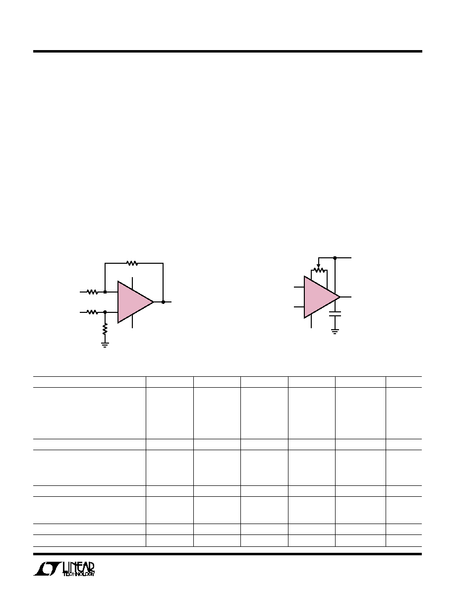
C
S
1
3
2
10k
POT
8
7
6
+
≠
LT1097
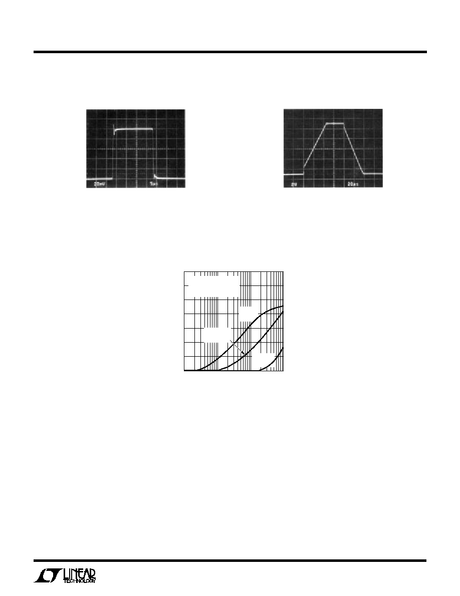
Frequency Compensation and Optional Offset Nulling
±
27V Common Mode Range Difference Amplifier
APPLICATIO
N
S I
N
FOR
M
ATIO
N
W
U
U
U
Guaranteed Perfomance, V
S
=
±
15V, T
A
= 25
∞
C
PARAMETER
LT1097CN8
OP-77GP
AD707JN
OP-177GP
OP-97FP
UNITS
Error Terms
V
OS
Max
50
100
90
60
75
µ
V
I
OS
Max∑25k
6
70
50
70
4
µ
V
Gain Min, 10V Out
14
5
3
5
50
µ
V
CMRR, Min,
±
25V In
22
20
13
22
39
µ
V
PSRR, Min, V
S
=
±
15V
±
10%
6
9
9
9
9
µ
V
Sum of All Error Terms
98
204
165
166
177
µ
V
0.1Hz to 10Hz Noise
Voltage Noise
0.5
0.38
0.23
0.38
0.5
µ
Vp-p Typ
Current Noise∑50k
0.11
0.75
0.7
0.75
0.1
µ
Vp-p Typ
Resistor Noise
0.55
0.55
0.55
0.55
0.55
µ
Vp-p Typ
RMS sum
0.75
1
0.92
1
0.75
µ
Vp-p
Drift with Temp
TCV
OS
Max
1
1.2
1
1.2
2
µ
V/
∞
C
TCI
OS
Max∑25k
0.1
2.1
1
2.1
0.2
µ
V/
∞
C
Sum of Drift Terms
1.1
3.3
2
3.3
2.2
µ
V/
∞
C
Supply Current Max
0.56
2
3
2
0.6
mA
The LT1097 is pin compatible to and directly replaces such
precision op amps as the OP-07, OP-77, AD707, OP-97, OP-
177, LM607 and LT1001 with improved price/performance.
Compatibility includes externally nulling the offset voltage, as
all of the above devices are trimmed with a potentiometer
between Pin 1 and Pin 8 and the wiper tied to V
+
.
The simple difference amplifier can be used to illustrate
the all-around excellence of the LT1097. The 50k input
resistance is selected to be large enough compared to
input signal source resistance. Simultaneously, the 50k
resistors should not dominate the precision and noise
error budget. Assuming perfect matching between the
four resistors, the following table summarizes the input
referred performance obtained using the LT1097 and
other popular, low cost precision op amps.
Input offset voltage can be adjusted over a
±
600
µ
V range
with a 10k potentiometer.
The LT1097 is internally compensated for unity gain
stability. As shown on the Capacitive Load Handling plot,
the LT1097 is stable with any capacitive load. However,
the overcompensation capacitor, C
S
, can be used to re-
duce overshoot with heavy capacitive loads, to narrow
noise bandwidth or to stabilize circuits with gain in the
feedback loop.
10
LT1097
APPLICATIO
N
S I
N
FOR
M
ATIO
N
W
U
U
U
OUT
LT1097∑F03
5
0.01
µ
F
3
IN
2
6
50pF
10k
5k
+
≠
LT1097
15V
≠15V
V
O
V
O
= 1000V
OS
*RESISTORS MUST HAVE LOW
THERMOELECTRIC POTENTIAL
LT1097∑F04
4
3
2
7
6
50k*
100
*
50k*
+
≠
LT1097
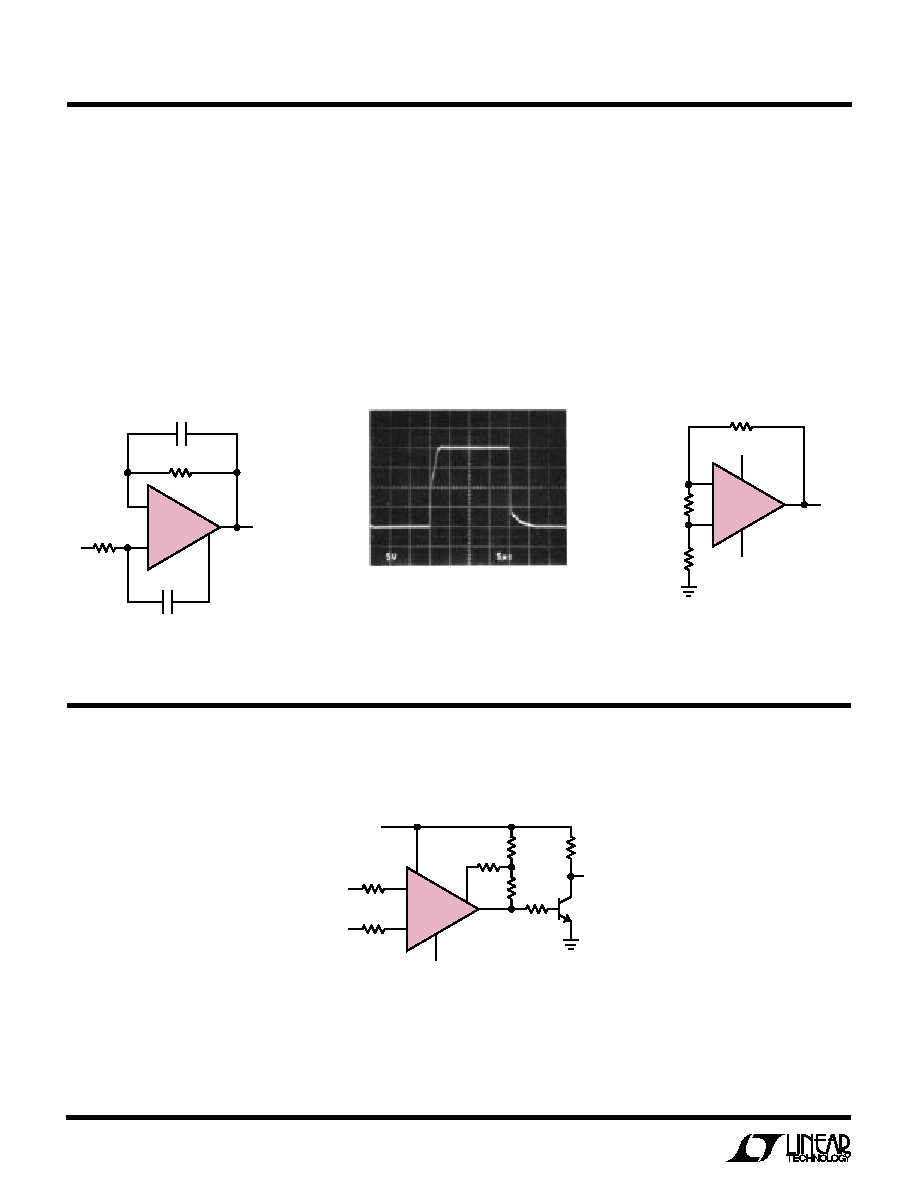
Pulse Response of Feedforward
Compensation
Test Circuit for Offset Voltage and
its Drift with Temperature
Follower Feedforward
Compensation
5
µ
s/DIV
5V/DIV
1097 G20
The availability of the compensation terminal permits the use
of feedforward frequency compensation to enhance slew
rate. The voltage follower feedforward scheme bypasses the
amplifier's gain stages and slews at nearly 10V/
µ
s.
The inputs of the LT1097 are protected with back-to-back
diodes. In the voltage follower configuration, when the
input is driven by a fast, large signal pulse (>1V), the input
protection diodes effectively short the output to the input
during slewing, and a current, limited only by the output
short circuit protection will flow through the diodes.
The use of a feedback resistor, as shown in the voltage
follower feedforward diagram, is recommended because
this resistor keeps the current below the short circuit limit,
resulting in faster recovery and settling of the output.
≠5V
OUT
2N3904
620k
LT1097∑TA02
4
3
2
1
7
5V
6
1k
330k
100k
10k
10k
≠IN
+IN
+
≠
LT1097
100k
Low Power Comparator with <10
µ
V Hysteresis
U
TYPICAL APPLICATIO
11
LT1097
Information furnished by Linear Technology Corporation is believed to be accurate and reliable.
However, no responsibility is assumed for its use. Linear Technology Corporation makes no represen-
tation that the interconnection of its circuits as described herein will not infringe on existing patent rights.
PACKAGE DESCRIPTIO
N
U
Dimensions in inches (millimeters) unless otherwise noted.
N8 1197
0.100
±
0.010
(2.540
±
0.254)
0.065
(1.651)
TYP
0.045 ≠ 0.065
(1.143 ≠ 1.651)
0.130
±
0.005
(3.302
±
0.127)
0.020
(0.508)
MIN
0.018
±
0.003
(0.457
±
0.076)
0.125
(3.175)
MIN
1
2
3
4
8
7
6
5
0.255
±
0.015*
(6.477
±
0.381)
0.400*
(10.160)
MAX
0.009 ≠ 0.015
(0.229 ≠ 0.381)
0.300 ≠ 0.325
(7.620 ≠ 8.255)
0.325
+0.035
≠0.015
+0.889
≠0.381
8.255
(
)
*THESE DIMENSIONS DO NOT INCLUDE MOLD FLASH OR PROTRUSIONS.
MOLD FLASH OR PROTRUSIONS SHALL NOT EXCEED 0.010 INCH (0.254mm)
1
2
3
4
0.150 ≠ 0.157**
(3.810 ≠ 3.988)
8
7
6
5
0.189 ≠ 0.197*
(4.801 ≠ 5.004)
0.228 ≠ 0.244
(5.791 ≠ 6.197)
0.016 ≠ 0.050
0.406 ≠ 1.270
0.010 ≠ 0.020
(0.254 ≠ 0.508)
◊
45
∞
0
∞
≠ 8
∞
TYP
0.008 ≠ 0.010
(0.203 ≠ 0.254)
SO8 0996
0.053 ≠ 0.069
(1.346 ≠ 1.752)
0.014 ≠ 0.019
(0.355 ≠ 0.483)
0.004 ≠ 0.010
(0.101 ≠ 0.254)
0.050
(1.270)
TYP
DIMENSION DOES NOT INCLUDE MOLD FLASH. MOLD FLASH
SHALL NOT EXCEED 0.006" (0.152mm) PER SIDE
DIMENSION DOES NOT INCLUDE INTERLEAD FLASH. INTERLEAD
FLASH SHALL NOT EXCEED 0.010" (0.254mm) PER SIDE
*
**
N8 Package
8-Lead PDIP (Narrow 0.300)
(LTC DWG # 05-08-1510)
S8 Package
8-Lead Plastic Small Outline (Narrow 0.150)
(LTC DWG # 05-08-1610)
12
LT1097
1097fas sn1097 LT/TP 0398 2K REV A ∑ PRINTED IN USA
©
LINEAR TECHNOLOGY CORPORATION 1989
Linear Technology Corporation
1630 McCarthy Blvd., Milpitas, CA 95035-7417
q
(408) 432-1900
FAX: (408) 434-0507
q
TELEX: 499-3977
q
www.linear-tech.com
RELATED PARTS
PART NUMBER
DESCRIPTION
COMMENTS
LT1490/LT1491
Dual/Quad General Purpose Micropower Rail-to-Rail Op Amps
Over-The-Top
TM
Inputs, 50
µ
A Supply Current Per
Amplifier, 2V to 44V Supply Range, 180kHz GBW
LT1492/LT1493
Dual/Quad 5MHz Low Power Single Supply Op Amps
180
µ
V V
OS
Max, 3V/
µ
s Slew Rate, 550
µ
A Supply Per
Amplifier
LT1077
Single Micropower Low V
OS
Op Amp
60
µ
V V
OS
Max, 68
µ
A Supply Current, 230kHz GBW,
Optimized for 5V Supplies
≠5V
1k*
1000pF
LT1097∑TA03
4
5
3
2
7
6
9k*
15V
100k
5%
10k
90k
900k
9M
0.1V
IN
10V
1V
100V
1000V
0.1V
10V
1V
100V
1000V
TO 1V FULL SCALE
ANALOG DIGITAL
CONVERTER
*RATIO MATCH
±
0.01%
FN507
ALLEN BRADLEY
DECADE VOLTAGE
DIVIDER
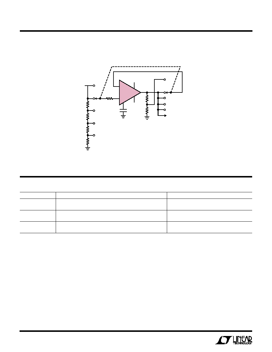
THIS APPLICATION REQUIRES LOW BIAS
CURRENT AND OFFSET VOLTAGE, LOW NOISE,
AND LOW DRIFT WITH TIME AND TEMPERATURE.
+
≠
LT1097
Input Amplifier for 4 1/2 Digit Voltmeter
U
TYPICAL APPLICATIO
Over-The-Top is a trademark of Linear Technology Corporation.