1
LT1101
1101fa
Gain Error: 0.04% Max
Gain Nonlinearity: 0.0008% (8ppm) Max
Gain Drift: 4ppm/∞C Max
Supply Current: 105µA Max
Offset Voltage: 160µV Max
Offset Voltage Drift: 0.4µV/∞C Typ
Offset Current: 600pA Max
CMRR, G = 100: 100dB Min
0.1Hz to 10Hz Noise: 0.9µVp-p Typ
2.3pAp-p Typ
Gain Bandwidth Product: 250kHz Min
Single or Dual Supply Operation
Surface Mount Package Available
The LT
Æ
1101 establishes the following milestones:
(1) It is the first micropower instrumentation amplifier,
(2) It is the first single supply instrumentation amplifier,
(3) It is the first instrumentation amplifier to feature fixed
gains of 10 and/or 100 in low cost, space-saving 8-lead
packages.
The LT1101 is completely self-contained: no external gain
setting resistor is required. The LT1101 combines its
micropower operation (75µA supply current) with a
gain error of 0.008%, gain linearity of 3ppm, gain drift of
1ppm/∞C. The output is guaranteed to drive a 2k load to
±10V with excellent gain accuracy.
Other precision specifications are also outstanding:
50µV input offset voltage, 130pA input offset current, and
low drift (0.4µV/∞C and 0.7pA/∞C). In addition, unlike other
instrumentation amplifiers, there is no output offset
voltage contribution to total error.
A full set of specifications are provided with ±15V dual
supplies and for single 5V supply operation. The LT1101
can be operated from a single lithium cell or two Ni-Cad
batteries. Battery voltage can drop as low as 1.8V, yet the
LT1101 still maintains its gain accuracy. In single supply
applications, both input and output voltages swing
to within a few millivolts of ground. The output sinks
current while swinging to ground--no external, power
consuming pull down resistors are needed.
Precision, Micropower,
Single Supply Instrumentation
Amplifier (Fixed Gain = 10 or 100)
FEATURES
APPLICATIO S
U
DESCRIPTIO
U
Differential Signal Amplification in Presence of
Common Mode Voltage
Micropower Bridge Transducer Amplifier
≠ Thermocouples
≠ Strain Gauges
≠ Thermistors
Differential Voltage-to-Current Converter
Transformer Coupled Amplifier
4mA to 20mA Bridge Transmitter
, LTC and LT are registered trademarks of Linear Technology Corporation.
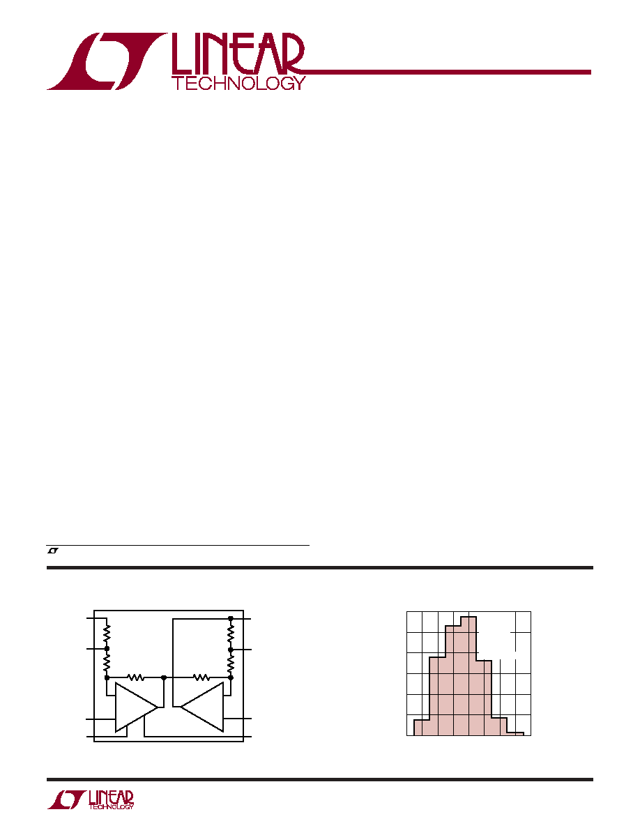
Gain Error Distribution
GAIN ERROR (%)
≠0.04
0
PERCENT OF UNITS
5
10
15
20
≠0.02
0
0.02
0.04
25
30
≠0.03
≠0.01
0.01
0.03
LT1101 ∑ TA02
930 UNITS
TESTED
IN ALL PACKAGES
G = 100
R
L
= 50k
T
A
= 25∞C
TYPICAL APPLICATIO
U
≠
+
≠
+
LT1101 ∑ TA01
OUTPUT
90R
9R
90R
9R
R
A
B
R 9.2k
R
V
+
V
≠
INVERTING
INPUT
GROUND PIN 1, OUTPUT AT PIN 8
G = 100: NO ADDITIONAL CONNECTIONS
G = 10: SHORT PIN 2 TO PIN 1, SHORT PIN 7 TO PIN 8
SHORT TO 1,
G = 10
N.C. G = 100
GROUND
(REF)
8
7
6
5
4
3
2
1
SHORT TO 8
G = 10
N.C. G = 100
NONINVERTING
INPUT
2
LT1101
1101fa
ABSOLUTE AXI U RATI GS
W
W
W
U
Supply Voltage ...................................................... ±22V
Differential Input Voltage ....................................... ±36V
Input Voltage ............... Equal to Positive Supply Voltage
..........10V Below Negative Supply Voltage
Output Short Circuit Duration .......................... Indefinite
(Note 1)
Operating Temperature Range
LT1101AM/LT1101M (OBSOLETE) ... ≠ 55∞C to 125∞C
LT1101AI/LT1101I .............................. ≠ 40∞C to 85∞C
LT1101AC/LT1101C ................................ 0∞C to 70∞C
Storage Temperature Range ................. ≠ 65∞C to 150∞C
Lead Temperature (Soldering, 10 sec).................. 300∞C
PACKAGE/ORDER I FOR ATIO
U
U
W
Consult LTC Marketing for parts specified with wider operating temperature ranges.
LT1101AIN8
LT1101IN8
LT1101ACN8
LT1101CN8
LT1101SW
LT1101ISW
OBSOLETE PACKAGES
Consider the N8 as an Alternate Source
LT1101AMH
LT1101MH
LT1101ACH
LT1101CH
ORDER PART
NUMBER
ORDER PART
NUMBER
ORDER PART
NUMBER
OUT
G = 10
REF
G = 10
1
2
3
4
5
6
7
8
TOP VIEW
16
15
14
13
12
11
10
9
NC
GND (REF)
NC
≠IN
NC
V ≠
NC
NC
NC
NC
V +
NC
OUTPUT
+IN
+
≠
+
≠
R
9.2k
90R
9R
90R
9R
R
R
SW PACKAGE
16-LEAD PLASTIC SO
T
JMAX
= 150
∞
C,
JA
= 100
∞
C/W
+
≠
+
≠
1
2
3
4
5
6
7
8
TOP VIEW
V ≠
≠IN
OUTPUT
OUT
G = 10
REF
G = 10
GROUND
(REF)
+IN
R
9.2k
90R
9R
90R
9R
R
R
V +
T
JMAX
= 150
∞
C,
JA
= 130
∞
C/W
TOP VIEW
OUT
G = 10
OUTPUT
REF
G = 10
+IN
90R
90R
R
R
9R
9R
V
+
≠IN
V
≠
(CASE)
GROUND
(REF)
8
7
6
5
3
2
1
4
H PACKAGE
8-LEAD TO-5 METAL CAN
+
≠
+
≠
T
JMAX
= 150
∞
C,
JA
= 150
∞
C/W,
JC
= 45
∞
C/W
LT1101AMJ8
LT1101MJ8
LT1101ACJ8
LT1101CJ8
T
JMAX
= 150
∞
C,
JA
= 100
∞
C/W
N PACKAGE 8-LEAD PDIP
J PACKAGE 8-LEAD CERDIP
ELECTRICAL CHARACTERISTICS
LT11O1AM/AI/AC
LT1101M/I/C
SYMBOL
PARAMETER
CONDITIONS
MIN
TYP
MAX
MIN
TYP
MAX
UNITS
G
E
Gain Error
G = 100, V
0
= 0.1V to 3.5V, R
L
= 50k
0.010
0.050
0.011
0.075
%
G = 10, V
0
= 0.1V to 3.5V, R
L
= 50k
0009
0.040
0.010
0.060
%
G
NL
Gain Nonlinearity
G = 100, R
L
= 50k
20
60
20
75
ppm
G = 10, R
L
= 50k (Note 2)
3
7
3
8
ppm
V
OS
Input Offset Voltage
50
160
60
220
µV
LT1101SW
250
600
µV
l
OS
Input Offset Current
0.13
0.60
0.15
0.90
nA
I
B
Input Bias Current
6
8
6
10
nA
I
S
Supply Current
75
105
78
120
µA
V
S
= 5V, 0V, V
CM
= 0.1V, V
REF(PIN 1)
= 0.1V, G = 10 or 100, T
A
= 25∞C, unless
otherwise noted. (Note 4)

4
LT1101
1101fa
ELECTRICAL CHARACTERISTICS
LT1101AM/AI
LT1101M/I
SYMBOL
PARAMETER
CONDITIONS
MIN
TYP
MAX
MIN
TYP
MAX
UNITS
V
O
Maximum 0utput
R
L
= 50k
13.0
14.2
13.0
14.2
V
Voltage Swing
R
L
= 2k
11.0
13.2
11.0
13.2
V
BW
Bandwidth
G = 100 (Note 2)
2.3
3.5
2.3
3.5
kHz
G = 10 (Note 2)
25
37
25
37
kHz
SR
Slew Rate
0.06
0.10
0.06
0.10
V/µs
V
S
= ±15V, V
CM
= 0V, T
A
= 25∞C, Gain = 10 or 100, unless otherwise noted.
LT1101AM/AI
LT1101M/I
SYMBOL
PARAMETER
CONDITIONS
MIN
TYP
MAX
MIN
TYP
MAX
UNITS
G
E
Gain Error
G = 100, V
O
= ±10V, R
L
= 50k
0.024
0.070
0.026
0.100
%
G = 100, V
O
= ±10V, R
L
= 5k
0.030
0.100
0.035
0.130
%
G = 10, V
O
= ±10V, R
L
= 50k or 5k
0.015
0.070
0.018
0.100
%
TCG
E
Gain Error Drift
G = 100, R
L
= 50k
2
4
2
5
ppm/∞C
(Note 2)
G = 100, R
L
= 5k
2
7
2
8
ppm/∞C
G = 10, R
L
= 50k or 5k
1
4
1
5
ppm/∞C
G
NL
Gain Nonlinearity
G = 100, R
L
= 50k
24
70
26
90
ppm
G = 100, R
L
= 5k
70
300
75
500
ppm
G = 10, R
L
= 50k
4
13
5
15
ppm
G = 10, R
L
= 5k
10
40
12
60
ppm
V
OS
Input Offset Voltage
90
350
110
500
µV
LT1101ISW
110
950
µV
V
OS
/T Input Offset Voltage Drift
(Note 2)
0.4
2.0
0.5
2.8
µV/∞C
LT1101ISW
0.5
4.8
mV/∞C
l
OS
Input Offset Current
0.16
0.80
0.19
1.30
nA
l
OS
/T
Input Offset Current Drift
(Note 2)
0.5
4.0
0.8
7.0
pA/∞C
I
B
Input Bias Current
7
10
7
12
nA
I
B
/T
Input Bias Current Drift
(Note 2)
10
25
10
30
pA/∞C
CMRR
Common Mode
G = 100, V
CM
= ≠14.4V to 13V
96
111
94
111
dB
Rejection Ratio
G = 100, V
CM
= ≠13V to 11.5V
80
99
78
98
dB
PSRR
Power Supply
V
S
= 3.0, ≠ 0.1V to ±18V
98
110
94
110
dB
Rejection Ratio
I
S
Supply Current
105
165
108
190
µA
V
O
Maximum 0utput
R
L
= 50k
12.5
14.0
12.5
14.0
V
Voltage Swing
R
L
= 5k
11.0
13.5
11.0
13.5
V
ELECTRICAL CHARACTERISTICS
V
S
= ±15V, V
CM
= 0V, Gain = 10 or 100, ≠55∞C T
A
125∞C for AM/M
grades, ≠40∞C T
A
85∞C for AI/I grades, unless otherwise noted.