1107 layout
1
LT1107
1107fa
FEATURES
APPLICATIO S
U
DESCRIPTIO
U
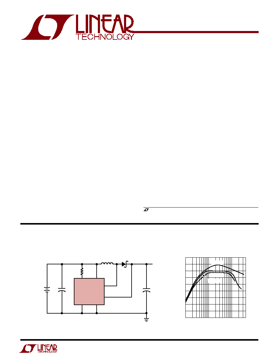
TYPICAL APPLICATIO
U
Micropower
DC/DC Converter
Adjustable and Fixed 5V, 12V
Efficiency
s
Operates at Supply Voltages from 2V to 30V
s
Consumes Only 320
µ
A Supply Current
s
Works in Step-Up or Step-Down Mode
s
Only Three External Components Required
s
Low-Battery Detector Comparator On-Chip
s
User Adjustable Current Limit
s
Internal 1A Power Switch
s
Fixed or Adjustable Output Voltage Versions
s
Space Saving 8-Pin MiniDIP or SO-8 Package
The LT
®
1107 is a versatile micropower DC/DC converter.
The device requires only three external components to
deliver a fixed output of 5V or 12V. Supply voltage ranges
from 2V to 12V in step-up mode and to 30V in step-down
mode. The LT1107 functions equally well in step-up, step-
down, or inverting applications.
The LT1107 is pin-for-pin compatible with the LT1111, but
has a duty cycle of 70%, resulting in increased output
current in many applications. The LT1107 can deliver
150mA at 5V from a 2AA cell input and 5V at 300mA from
24V in step-down mode. Quiescent current is just 320
µ
A,
making the LT1107 ideal for power-conscious battery-
operated systems. The 63kHz oscillator is optimized to
work with surface mount inductors and capacitors.
Switch current limit can be programmed with a single
resistor. An auxiliary gain block can be configured as a
low-battery detector, linear post regulator, undervoltage
lock-out circuit, or error amplifier.
s
Palmtop Computers
s
3V to 5V, 5V to 12V Converters
s
24V to 5V, 12V to 5V Converters
s
LCD Bias Generators
s
Peripherals and Add-On Cards
s
Battery Backup Supplies
s
Cellular Telephones
s
Portable Instruments
LOAD CURRENT (mA)
1
EFFICIENCY (%)
82
80
78
76
74
72
70
68
66
64
10
100
400
1107 TA02
V
IN
= 3V
V
IN
= 2.5V
V
IN
= 2V
5V
150mA
MBRS120T3
L1*
33
µ
H
47
2
×
AA
ALKALINE
CELLS
100
µ
F
SUMIDA CD54-330K
COILCRAFT DT3316-473
*
I
LIM
V
IN
SENSE
SW1
SW2
GND
47
µ
F
LT1107-5
1107 TA01
+
+
Palmtop Computer Logic Supply
, LTC and LT are registered trademarks of Linear Technology Corporation
2
LT1107
1107fa
A
U
G
W
A
W
U
W
A
R
BSOLUTE
XI
TI
S
Supply Voltage (V
IN
) ............................................... 36V
SW1 Pin Voltage (V
SW1
) ......................................... 50V
SW2 Pin Voltage (V
SW2
) ............................ 0.5V to V
IN
Feedback Pin Voltage (LT1107) ................................ 5V
Sense Pin Voltage (LT1107-5, LT1107-12) ............ 36V
Maximum Power Dissipation ............................ 500mW
Set Pin Voltage ...................................................... 5.5V
Maximum Switch Current ...................................... 1.5A
Operating Temperature Range
LT1107C ................................................ 0
°
C to 70
°
C
LT1107I ............................................ 45
°
C to 85
°
C
LT1107M(OBSOLETE) ............... 55
°
C to 125
°
C
Storage Temperature Range ................. 65
°
C to 150
°
C
Lead Temperature (Soldering, 10 sec).................. 300
°
C
ELECTRICAL C
C
HARA TERISTICS
The
q
denotes the specifications which apply over the full operating
temperature range, V
IN
= 3V, military or commercial version, T
A
= 25
°
C, unless otherwise noted.
SYMBOL
PARAMETER
CONDITIONS
MIN
TYP
MAX
UNITS
I
Q
Quiescent Current
Switch OFF
320
450
µ
A
Quiescent Current, Step-Up Mode Configuration
No Load
LT1107-5
360
µ
A
LT1107-12
550
µ
A
V
IN
Input Voltage
Step-Up Mode
q
2
12.6
V
Step-Down Mode
q
30.0
V
Comparator Trip Point Voltage
LT1107 (Note 2)
q
1.2
1.25
1.3
V
V
OUT
Output Sense Voltage
LT1107-5 (Note 3)
q
4.75
5
5.25
V
LT1107-12 (Note 3)
q
11.40
12
12.60
V
Comparator Hysteresis
LT1107
q
8
12.5
mV
Output Hysteresis
LT1107-5
q
32
50
mV
LT1107-12
q
75
120
mV
f
OSC
Oscillator Frequency
50
63
77
kHz
Duty Cycle, Step-Up Mode
Full Load
64
70
76
%
t
ON
Switch ON Time, Step-Up Mode
I
LIM
Tied to V
IN
8.8
11
12.7
µ
s
W
U
U
PACKAGE/ORDER I FOR ATIO
ORDER PART
NUMBER
ORDER PART
NUMBER
LT1107CN8
LT1107CN8-5
LT1107CN8-12
LT1107CS8
LT1107CS8-5
LT1107CS8-12
LT1107IS8
T
JMAX
= 90
°
C,
JA
= 130
°
C/W (N)
T
JMAX
= 90
°
C,
JA
= 150
°
C/W
1107
11075
110712
1107I
S8 PART MARKING
1
2
3
4
8
7
6
5
TOP VIEW
I
LIM
V
IN
SW1
SW2
FB (SENSE)*
SET
AO
GND
N8 PACKAGE
8-LEAD PLASTIC DIP
* FIXED VERSIONS
1
2
3
4
8
7
6
5
TOP VIEW
S8 PACKAGE
8-LEAD PLASTIC SO
*FIXED VERSIONS
I
LIM
V
IN
SW1
SW2
FB(SENSE)*
SET
AO
GND
Consult LTC Marketing for parts specified with wider operating temperature ranges.
(Note 1)
J8 PACKAGE
8-LEAD CERAMIC DIP
T
JMAX
= 150
°
C,
JA
= 120
°
C/W (J)
LT1107MJ8
LT1107MJ8-5
LT1107MJ8-12
OBSOLETE PACKAGE
Consider the N8 Package for Alternate Source
3
LT1107
1107fa
LT1107C
SYMBOL
PARAMETER
CONDITIONS
MIN
TYP
MAX
UNITS
I
Q
Quiescent Current
Switch OFF
q
450
µ
A
f
OSC
Oscillator Frequency
q
50
63
88
kHz
DC
Duty Cycle
Step-Up Mode
q
62
69
78
%
Step-Down Mode, V
IN
= 12V
q
50
60
70
%
t
ON
Switch ON Time
Step-Up Mode
q
8
11
13.5
µ
s
Step-Down Mode, V
IN
= 12V
q
6
9
12.0
µ
s
Reference Line Regulation
2V
V
IN
5V
q
0.2
0.7
%/V
V
SAT
Switch Saturation Voltage, Step-Up Mode
V
IN
= 3V, I
SW
= 650mA
q
0.5
0.65
V
Switch Saturation Voltage, Step-Down Mode
V
IN
= 12V, I
SW
= 650mA
q
1.1
1.5
V
ELECTRICAL C
C
HARA TERISTICS
The
q
denotes the specifications which apply over the full operating temperature range, V
IN
= 3V, 55
°
C
T
A
125
°
C, unless
otherwise noted.
Note 1: Absolute Maximum Ratings are those values beyond which the life
of a device may be impaired.
Note 2: This specification guarantees that both the high and low trip points
of the comparator fall within the 1.2V to 1.3V range.
Note 3: The output voltage waveform will exhibit a sawtooth shape due to
the comparator hysteresis. The output voltage on the fixed-output versions
will always be within the specified range.
Note 4: 100k resistor connected between a 5V source and the AO pin.
The
q
denotes the specifications which apply over the full operating
temperature range, V
IN
= 3V, military or commercial version, T
A
= 25
°
C, unless otherwise noted.
The
q
denotes the specifications which apply over the full operating temperature range, V
IN
= 3V, 0
°
C
T
A
70
°
C, unless otherwise
noted.
SYMBOL
PARAMETER
CONDITIONS
MIN
TYP
MAX
UNITS
Feedback Pin Bias Current
LT1107, V
FB
= 0V
q
70
120
nA
Set Pin Bias Current
V
SET
= V
REF
q
70
300
nA
V
OL
Gain Block Output Low
I
SINK
= 300
µ
A, V
SET
= 1V
q
0.15
0.4
V
Reference Line Regulation
5V
V
IN
30V
q
0.02
0.075
%/V
A
V
Gain Block Gain
R
L
= 100k (Note 4)
q
1000
6000
V/V
Current Limit
220
to I
LIM
to V
IN
400
mA
Current Limit Temperature Coefficient
q
0.3
%/
°
C
Switch OFF Leakage Current
Measured at SW1 Pin, V
SW1
= 12V
1
10
µ
A
V
SW2
Maximum Excursion Below GND
I
SW1
10
µ
A, Switch OFF
400
350
mV
LT1107M
SYMBOL
PARAMETER
CONDITIONS
MIN
TYP
MAX
UNITS
I
Q
Quiescent Current
Switch OFF
q
500
µ
A
f
OSC
Oscillator Frequency
q
40
63
95
kHz
DC
Duty Cycle
Step-Up Mode
q
56
69
81
%
Step-Down Mode, V
IN
= 12V
q
45
60
73
%
t
ON
Switch ON Time
Step-Up Mode
q
7
11
15
µ
s
Step-Down Mode, V
IN
= 12V
q
5
9
13
µ
s
Reference Line Regulation
2V
V
IN
5V, 0
°
C
T
A
125
°
C
0.2
0.4
%/V
2.4V
V
IN
5V, T
A
= 55
°
C
0.8
%/V
V
SAT
Switch Saturation Voltage, Step-Up Mode
0
°
C
T
A
125
°
C, I
SW
= 500mA
0.5
0.65
V
T
A
= 55
°
C, I
SW
= 400mA
0.5
0.65
V
Switch Saturation Voltage, Step-Down Mode
V
IN
= 12V, I
SW
= 500mA
0
°
C
T
A
125
°
C
1.5
V
T
A
= 55
°
C
2.0
V
4
LT1107
1107fa
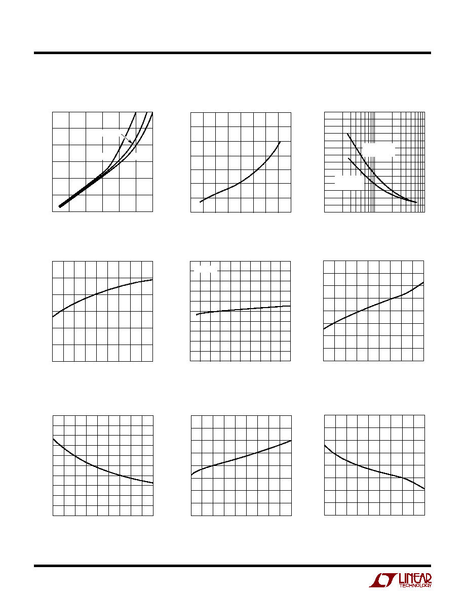
C
C
HARA TERISTICS
U
W
A
TYPICAL PERFOR
CE
Saturation Voltage, Step-Up Mode
Switch ON Voltage, Step-Down
(SW2 Pin Grounded)
Mode (SW1 Pin Connected to V
IN
) Maximum Switch Current vs R
LIM
Quiescent Current
Quiescent Current
TEMPERATURE (
°
C)
55
FREQUENCY (kHz)
15
25
45
125
1107 G07
35
5
65
85 105
100
90
80
70
60
50
40
30
20
Oscillator Frequency
Switch ON Time
Step-Down Mode
TEMPERATURE (
°
C)
55
SWITCH ON TIME (
µ
s)
15
25
45
125
1107 G10
35
5
65
85 105
13
12
11
10
9
8
7
6
5
TEMPERATURE (
°
C)
55
DUTY CYCLE (%)
15
25
45
125
1107 G09
35
5
65
85 105
85
80
75
70
65
60
55
50
45
Duty Cycle
Step-Up Mode
TEMPERATURE (
°
C)
55
QUIESCENT CURRENT (
µ
A)
15
25
45
125
1107 G05
35
5
65
85 105
400
350
300
250
200
150
100
TEMPERATURE (
°
C)
55
SWITCH ON TIME (
µ
s)
15
25
45
125
1107 G08
35
5
65
85 105
16
15
14
13
12
11
10
9
8
7
6
Switch ON Time
Step-Up Mode
INPUT VOLTAGE (V)
0
QUIESCENT CURRENT (
µ
A)
400
380
360
340
320
300
280
260
240
220
200
24
1107 G06
6
12
18
30
3
9
15
21
27
T
A
= 25
°
C
R
LIM
(
)
SWITCH CURRENT (A)
10
1107 G03
100
1.5
1.4
1.3
1.2
1.1
0.9
0.8
1000
0.7
0.6
0.5
0.4
0.3
0.2
0.1
1.0
STEP-DOWN
V
IN
= 12V
STEP-UP
2V
V
IN
5V
SWITCH CURRENT (A)
0
SWITCH ON VOLTAGE (V)
0.6
1107 G02
0.2
0.4
0.8
1.4
1.3
1.2
1.1
1.0
0.9
0.8
0.7
0.1
0.3
0.5
0.7
SWITCH CURRENT (A)
0
SATURATION VOLTAGE (V)
1.2
1.0
0.8
0.6
0.4
0.2
0
0.2
0.4
0.6
0.8
1107 G01
1.0
1.2
V
IN
= 3V
V
IN
= 2V
V
IN
= 5V
5
LT1107
1107fa
I
LIM
(Pin 1): Connect this pin to V
IN
for normal use. Where
lower current limit is desired, connect a resistor between
I
LIM
and V
IN
. A 220
resistor will limit the switch current
to approximately 400mA.
V
IN
(Pin 2): Input Supply Voltage.
SW1 (Pin 3):
Collector of Power Transistor. For step-up
mode connect to inductor/diode. For step-down mode
connect to V
IN
.
SW2 (Pin 4):
Emitter of Power Transistor. For step-up
mode connect to ground. For step-down mode connect to
inductor/diode. This pin must never be allowed to go more
than a Schottky diode drop below ground.
GND (Pin 5): Ground.
AO (Pin 6): Auxiliary Gain Block (GB) Output. Open collector,
can sink 300
µ
A.
SET (Pin 7): GB Input. GB is an op amp with positive input
connected to SET pin and negative input connected to
1.25V reference.
FB/SENSE (Pin 8): On the LT1107 (adjustable), this pin
goes to the comparator input. On the LT1107-5 and
LT1107-12, this pin goes to the internal application resistor
that sets output voltage.
PI
U
FU
U
C
U
S
O
TI
C
C
HARA TERISTICS
U
W
A
TYPICAL PERFOR
CE
Minimum/Maximum Frequency
Minimum/Maximum Frequency
vs ON Time, Step-Down Mode
vs ON Time, Step-Up Mode
TEMPERATURE (
°
C)
55
DUTY CYCLE (%)
15
25
45
125
1107 G13
35
5
65
85 105
70
65
60
55
50
45
40
35
TEMPERATURE (
°
C)
55
OUTPUT VOLTAGE (V)
15
25
45
125
1107 G16
35
5
65
85 105
5.3
5.2
5.1
5.0
4.9
4.8
4.7
TEMPERATURE (
°
C)
55
OUTPUT VOLTAGE (V)
15
25
45
125
1107 G17
35
5
65
85 105
12.20
12.15
12.10
12.05
12.00
11.95
11.90
11.85
11.80
LT1107-5
LT1107-12
LT1107
Output Voltage
Output Voltage
Feedback Voltage
TEMPERATURE (
°
C)
55
TRIP POINT VOLTAGE (V)
15
25
45
125
1107 G18
35
5
65
85 105
1.30
1.29
1.28
1.27
1.26
1.25
1.24
1.23
1.22
1.21
1.20
ON TIME (
µ
s)
4
FREQUENCY (kHz)
100
90
80
70
60
50
40
30
5
9
11
1107 G11
8
13 14
6
7
10
12
0
°
C
T
A
70
°
C
55
°
C
T
A
125
°
C
ON TIME (
µ
s)
6
FREQUENCY (kHz)
100
90
80
70
60
50
40
30
7
11
13
1107 G12
10
15 16
8
9
12
14
0
°
C
T
A
70
°
C
55
°
C
T
A
125
°
C
T
A
= 25
°
C
Duty Cycle
Step-Down Mode