 | –≠–ª–µ–∫—Ç—Ä–æ–Ω–Ω—ã–π –∫–æ–º–ø–æ–Ω–µ–Ω—Ç: LT1108CN8 | –°–∫–∞—á–∞—Ç—å:  PDF PDF  ZIP ZIP |

1
LT1108
Micropower
DC/DC Converter
Adjustable and Fixed 5V, 12V
D
U
ESCRIPTIO
S
FEATURE
The LT1108 is a versatile micropower DC/DC converter.
The device requires only four external components to
deliver a fixed output of 5V or 12V. Supply voltage ranges
from 2V to 12V in step-up mode and to 30V in step-down
mode. The LT1108 functions equally well in step-up, step-
down, or inverting applications.
The LT1108 is pin-for-pin compatible with the LT1173, but
has a duty cycle of 70%, resulting in increased output
current in many applications. The LT1108 can deliver
150mA at 5V from a 2 AA cell input and 5V at 300mA from
9V in step-down mode. Quiescent current is just 110
µ
A,
making the LT1108 ideal for power conscious battery-
operated systems.
Switch current limit can be programmed with a single
resistor. An auxiliary gain block can be configured as a low
battery detector, linear post regulator, undervoltage lock-
out circuit, or error amplifier.
s
Operates at Supply Voltages from 2V to 30V
s
Consumes Only 110
µ
A Supply Current
s
Works in Step-Up or Step-Down Mode
s
Only Four External Components Required
s
Low Battery Detector Comparator On-Chip
s
User Adjustable Current Limit
s
Internal 1A Power Switch
s
Fixed or Adjustable Output Voltage Versions
s
Space Saving 8-Pin MiniDIP or S8 Package
U
S
A
O
PPLICATI
s
Palmtop Computers
s
3V to 5V, 5V to 12V Converters
s
9V to 5V, 12V to 5V Converters
s
LCD Bias Generators
s
Peripherals and Add-On Cards
s
Battery Backup Supplies
s
Cellular Telephones
s
Portable Instruments
U
A
O
PPLICATI
TYPICAL
LOAD CURRENT (mA)
1
78
EFFICIENCY (%)
80
82
84
10
100
LT1108 ∑ TA02
76
74
72
70
V
IN
= 3V
V
IN
= 2.5V
V
IN
= 2V
AVX
TPS
330
µ
F
6.3V
L1*
100
µ
H
LT1108 ∑ TA01
1N5817
5V
150mA
GND
SW2
SW1
I
LIM
V
IN
LT1108-5
SENSE
100
µ
F
+
*L1 =
+
2
◊
AA
CELLS
GOWANDA GA20-103K
COILTRONICS CTX100-4
SUMIDA CD105-101K
47
Efficiency
Palmtop Computer Logic Supply
2
LT1108
A
U
G
W
A
W
U
W
A
R
BSOLUTE
XI
TI
S
Supply Voltage (V
IN
) ............................................... 36V
SW1 Pin Voltage (V
SW1
) ......................................... 50V
SW2 Pin Voltage (V
SW2
) ............................ ≠ 0.5V to V
IN
Feedback Pin Voltage (LT1108) ............................. 5.5V
Sense Pin Voltage (LT1108, -5, -12) ...................... 36V
Maximum Power Dissipation ............................ 500mW
Maximum Switch Current ...................................... 1.5A
Operating Temperature Range .................... 0
∞
C to 70
∞
C
Storage Temperature Range ................ ≠ 65
∞
C to 150
∞
C
Lead Temperature (Soldering, 10 sec) ................. 300
∞
C
W
U
U
PACKAGE/ORDER I FOR ATIO
ORDER PART
NUMBER
LT1108CS8
LT1108CS8-5
LT1108CS8-12
S8 PART MARKING
ORDER PART
NUMBER
LT1108CN8
LT1108CN8-5
LT1108CN8-12
T
JMAX
= 90
∞
C,
JA
= 150
∞
C/W
T
JMAX
= 90
∞
C,
JA
= 130
∞
C/W
1
2
3
4
8
7
6
5
TOP VIEW
I
LIM
V
IN
SW1
SW2
FB (SENSE*)
SET
A0
GND
N8 PACKAGE
8-LEAD PLASTIC DIP
*FIXED VERSIONS
1
2
3
4
8
7
6
5
TOP VIEW
I
LIM
V
IN
SW1
SW2
FB (SENSE*)
SET
A0
GND
S8 PACKAGE
8-LEAD PLASTIC SOIC
*FIXED VERSIONS
ELECTRICAL C
C
HARA TERISTICS
T
A
= 25
∞
C, V
IN
= 3V, unless otherwise noted.
SYMBOL
PARAMETER
CONDITIONS
MIN
TYP
MAX
UNITS
I
Q
Quiescent Current
Switch OFF
q
110
150
µ
A
Quiescent Current, Boost Mode Configuration
No Load
LT1108-5
135
µ
A
LT1108-12
250
µ
A
V
IN
Input Voltage
Step-Up Mode
q
2
12.6
V
Step-Down Mode
q
30.0
V
Comparator Trip Point Voltage
LT1108 (Note 1)
q
1.2
1.245
1.3
V
V
OUT
Output Sense Voltage
LT1108-5 (Note 2)
q
4.75
5
5.25
V
LT1108-12 (Note 2)
q
11.4
12
12.6
V
Comparator Hysteresis
LT1108
q
5
10
mV
Output Hysteresis
LT1108-5
q
20
40
mV
LT1108-12
q
50
100
mV
f
OSC
Oscillator Frequency
q
14
19
25
kHz
Duty Cycle
Full Load, Step-Up Mode
q
63
70
78
%
t
ON
Switch-ON Time
I
LIM
Tied to V
IN
, Step-Up Mode
q
28
36
48
µ
s
Feedback Pin Bias Current
LT1108, V
FB
= 0V
q
10
50
nA
Set Pin Bias Current
V
SET
= V
REF
q
20
100
nA
V
OL
Gain Block Output Low
I
SINK
= 100
µ
A, V
SET
= 1V
q
0.15
0.4
V
Reference Line Regulation
2V
V
IN
5V
q
0.20
0.400
%/V
5V
V
IN
30V
q
0.02
0.075
%/V
V
SAT
SW
SAT
Voltage, Step-Up Mode
V
IN
= 3V, I
SW
= 650mA
q
0.5
0.65
V
V
IN
= 5V, I
SW
= 1A
0.8
1.00
V
1108
10805
10812
3
LT1108
T
A
= 25
∞
C, V
IN
= 3V, unless otherwise noted.
ELECTRICAL C
C
HARA TERISTICS
SYMBOL
PARAMETER
CONDITIONS
MIN
TYP
MAX
UNITS
V
SAT
SW
SAT
Voltage, Step-Down Mode
V
IN
= 12V, I
SW
= 650mA
1.1
1.5
V
q
1.7
V
A
V
Gain Block Gain
R
L
= 100k (Note 3)
q
400
1000
V/ V
Current Limit
220
from I
LIM
to V
IN
400
mA
Current Limit Temperature Coefficient
q
≠ 0.3
%/
∞
C
Switch OFF Leakage Current
Measured at SW1 Pin
1
10
µ
A
V
SW2
Maximum Excursion Below GND
I
SW1
10
µ
A, Switch OFF
≠ 400
≠ 350
mV
Note 2: The output voltage waveform will exhibit a sawtooth shape due to
the comparator hysteresis. The output voltage on the fixed output versions
will always be within the specified range.
Note 3: 100k resistor connected between a 5V source and the A0 pin.
The
q
denotes specifications which apply over the full operating
temperature range.
Note 1: This specification guarantees that both the high and low trip points
of the comparator fall within the 1.2V to 1.3V range.
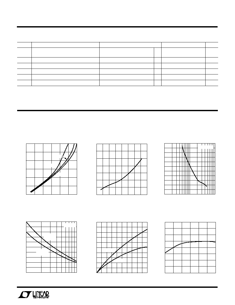
C
C
HARA TERISTICS
U
W
A
TYPICAL PERFOR
CE
R
LIM
(
)
10
SWITCH CURRENT (mA)
100
1000
LT1108 ∑ TPC03
1000
1200
1100
900
800
700
600
500
400
300
200
100
2V
V
IN
5V
Saturation Voltage Step-Up Mode
(SW2 Pin Grounded)
Switch ON Voltage
Step-Down Mode
(SW1 Pin Connected to V
IN
)
Maximum Switch Current
vs R
LIM
Saturation Voltage Step-Up Mode
(SW2 Pin Grounded)
R
LIM
(
)
100
0
SWITCH CURRENT (mA)
200
400
600
800
1000
LT1108 ∑ TPC04
100
300
500
700
900
1000
V
OUT
= 5V
V
IN
= 24V
L = 500
µ
H
V
IN
= 12V
L = 250
µ
H
Supply Current vs Switch Current
Quiescent Current
TEMPERATURE (∞C)
≠50
QUIESCENT CURRENT (
µ
A)
95
100
105
25
75
LT1108 ∑ TPC06
90
85
80
≠25
0
50
110
115
120
100
SWITCH CURRENT (A)
0
0
V
CESAT
(V)
0.2
0.4
0.6
0.8
1.2
0.2
0.4
0.6
0.8
LT1108 ∑ TPC01
1.0
1.2
1.0
V
IN
= 2V
V
IN
= 5V
V
IN
= 3V
SWITCH CURRENT (A)
0
SWITCH ON VOLTAGE (V)
1.1
1.2
1.3
0.6
LT1108 ∑ TPC02
1.0
0.9
0.2
0.4
0.8
0.8
0.7
1.4
0.5
0.1
0.3
0.7
SWITCH CURRENT (mA)
0
SUPPLY CURRENT (mA)
30
40
50
800
LTC1108 ∑ TPC05
20
10
0
200
400
600
1000
V
IN
= 5V
V
IN
= 2V
4
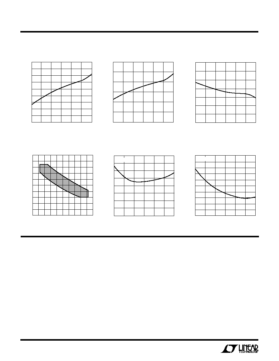
LT1108
C
C
HARA TERISTICS
U
W
A
TYPICAL PERFOR
CE
GND (Pin 5): Ground.
AO (Pin 6): Auxiliary gain block (GB) output. Open collector,
can sink 100
µ
A.
SET (Pin 7): GB input. GB is an op amp with positive input
connected to SET pin and negative input connected to
1.245V reference.
FB/SENSE (Pin 8): On the LT1108 (adjustable) this pin
goes to the comparator input. On the LT1108-5 and
LT1108-12, this pin goes to the internal application resistor
that sets output voltage.
Oscillator Frequency
Duty Cycle
Switch-ON Time
TEMPERATURE (∞C)
13
FREQUENCY (kHz)
14
16
17
18
22
LT1108 ∑ TPC07
15
19
20
21
≠50
25
75
≠25
0
50
100
TEMPERATURE (∞C)
50
DUTY CYCLE (%)
55
60
65
70
80
LT1108 ∑ TPC08
75
≠50
25
75
≠25
0
50
100
Minimum/Maximum Frequency
Switch Saturation Voltage
Switch Saturation Voltage
vs ON-Time
Step-Up Mode
Step-Down Mode
PI
U
FU
U
C
U
S
O
TI
I
LIM
(Pin 1): Connect this pin to V
IN
for normal use. Where
lower current limit is desired, connect a resistor between
I
LIM
and V
IN
. A 220
resistor will limit the switch current
to approximately 400mA.
V
IN
(Pin 2): Input supply voltage.
SW1 (Pin 3):
Collector of power transistor. For step-up
mode connect to inductor/diode. For step-down mode
connect to V
IN
.
SW2 (Pin 4):
Emitter of power transistor. For step-up
mode connect to ground. For step-down mode connect to
inductor/diode. This pin must never be allowed to go more
than a Schottky diode drop below ground.
TEMPERATURE (∞C)
≠50
38
40
42
25
75
LT1108 ∑ TPC09
36
34
≠25
0
50
100
32
30
SWITCH-ON TIME (
µ
s)
44
TEMPERATURE (∞C)
≠50
V
CESAT
(V)
0.3
0.4
0.5
25
75
LT1108 ∑ TPC11
0.2
0.1
0
≠25
0
50
0.6
0.7
0.8
100
I
SW
= 650mA
TEMPERATURE (∞C)
≠50
0.8
V
SAT
(V)
1.0
1.1
1.2
1.3
1.4
1.5
≠25
0
25
50
LT1108 ∑ TPC12
75
1.6
1.7
1.8
0.9
100
I
SW
= 650mA
ON-TIME (
µ
s)
25
FREQUENCY (kHz)
20
24
28
45
LT1108 ∑ TPC10
16
12
0
30
35
40
50
18
22
26
14
10
5
LT1108
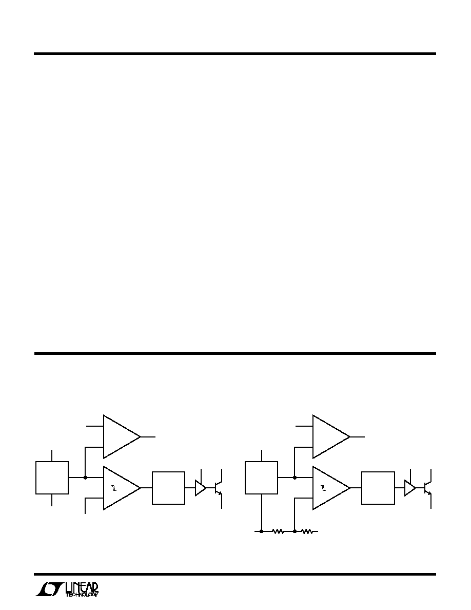
UO
ATI
1 OPER
negative input of A2 is the 1.245V reference. A resistor
divider from V
IN
to GND, with the mid-point connected to
the SET pin provides the trip voltage in a low battery
detector application. A0 can sink 100
µ
A (use a 47k resis-
tor pull-up to 5V).
A resistor connected between the I
LIM
pin and V
IN
sets
maximum switch current. When the switch current ex-
ceeds the set value, the switch cycle is prematurely
terminated. If current limit is not used, I
LIM
should be tied
directly to V
IN
. Propagation delay through the current-
limit circuitry is approximately 2
µ
s.
In step-up mode the switch emitter (SW2) is connected to
ground and the switch collector (SW1) drives the induc-
tor; in step-down mode the collector is connected to V
IN
and the emitter drives the inductor.
The LT1108-5 and LT1108-12 are functionally identical to
the LT1108. The -5 and -12 versions have on-chip voltage
setting resistors for fixed 5V or 12V outputs. Pin 8 on the
fixed versions should be connected to the output. No
external resistors are needed.
The LT1108 is a gated oscillator switcher. This type
architecture has very low supply current because the
switch is cycled when the feedback pin voltage drops
below the reference voltage. Circuit operation can best be
understood by referring to the LT1108 block diagram.
Comparator A1 compares the feedback (FB) pin voltage
with the 1.245V reference signal. When FB drops below
1.245V, A1 switches on the 19kHz oscillator. The driver
amplifier boosts the signal level to drive the output NPN
power switch. The switch cycling action raises the output
voltage and FB pin voltage. When the FB voltage is suffi-
cient to trip A1, the oscillator is gated off. A small amount
of hysteresis built into A1 ensures loop stability without
external frequency compensation. When the comparator
output is low, the oscillator and all high current circuitry
is turned off, lowering device quiescent current to just
110
µ
A.
The oscillator is set internally for 36
µ
s ON-time and 17
µ
s
OFF-time, allowing continuous mode operation in many
cases such as 2V to 5V converters. Continuous mode
greatly increases available output power.
Gain block A2 can serve as a low battery detector. The
W
I
D AGRA
BLOCK
S
LT1108
LT1108-5/LT1108-12
I
LIM
A2
A1
V
IN
GND
FB
SET
A0
GAIN BLOCK/
ERROR AMP
COMPARATOR
DRIVER
SW1
SW2
1.245V
REFERENCE
OSCILLATOR
LT1108 ∑ BD
I
LIM
A2
A1
V
IN
GND
SET
A0
GAIN BLOCK/
ERROR AMP
COMPARATOR
DRIVER
SW1
SW2
1.245V
REFERENCE
OSCILLATOR
LT1108-5 ∑ BD
SENSE
R1
R2
753k
LT1108-5: R1 = 250k
LT1108-12: R1 = 87.4k