Äîêóìåíòàöèÿ è îïèñàíèÿ www.docs.chipfind.ru
LT1109
1
Micropower Low Cost
DC/DC Converter
Adjustable and Fixed 5V, 12V
All Surface Mount
Flash Memory VPP Generator
U
S
A
O
PPLICATI
s
Flash Memory VPP Generators
s
3V to 5V Converters
s
5V to 12V Converters
s
Disk Drives
s
PC Plug-In Cards
s
Peripherals
s
Battery-Powered Equipment
U
A
O
PPLICATI
TYPICAL
s
Uses Off-the-Shelf Inductors
s
Only 33
µ
H Inductor Required
s
Low Cost
s
3-Lead TO-92, SO8, or 8-Pin DIP
s
Adjustable or Fixed 5V or 12V Output
s
120kHz Oscillator
s
Only Three External Components Required
s
320
µ
A I
Q
s
1.6V Minimum Start-Up Voltage
s
Logic Controlled Shutdown
D
U
ESCRIPTIO
S
FEATURE
The LT1109 is a simple step-up DC/DC converter. Avail-
able in 8-pin SO, 3-lead TO-92 (fixed output only) or
miniDIP packages, the devices require only three external
components to construct a complete DC/DC converter.
Current drain is just 320
µ
A at no load, making the device
ideal for cost-sensitive applications where standby cur-
rent must be kept to a minimum.
The LT1109-5 can deliver 5V at 100mA from a 3V input
and the LT1109-12 can deliver 12V at 60mA from a 5V
input. The 8-pin versions also feature a logic controlled
SHUTDOWN pin that turns off the oscillator when taken
low. The gated-oscillator design requires no frequency
compensation components. The high frequency 120kHz
oscillator permits the use of small surface mount induc-
tors and capacitors. For a 5V to 12V at 120mA converter,
see the LT1109A. Foa a 5V to 12V at 200mA converter
with 20
µ
A shutdown current, see the LT1301.
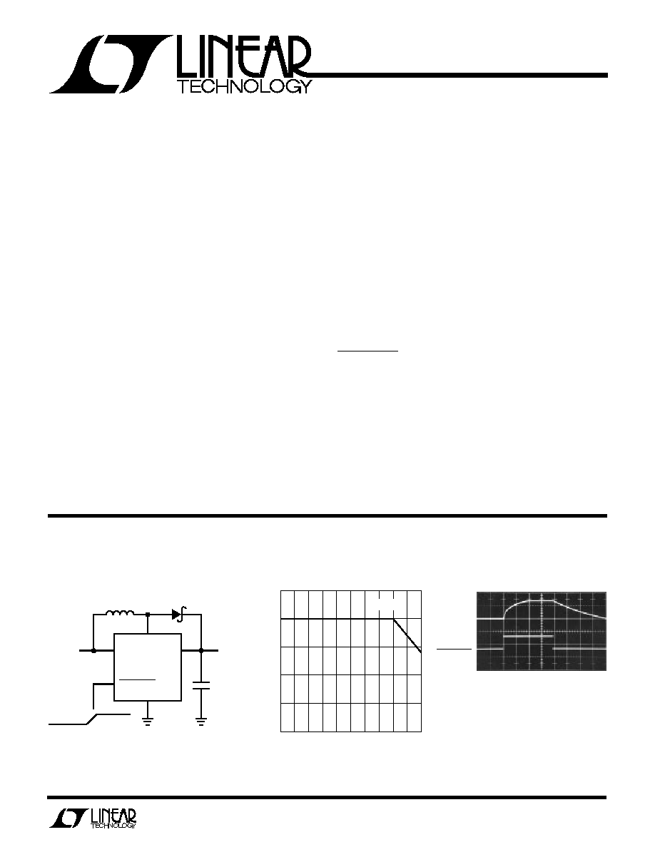
SHUTDOWN
5V/DIV
OV
V
OUT
5V/DIV
1ms/DIV
LT1109 · TA02
L1
LT1109 · TA01
+
GND
SW
SENSE
LT1109CS8-12
V
OUT
12V
80mA
MBRS120T3
V
IN
V
IN
5V
SHUTDOWN PROGRAM
SHUTDOWN*
* 8-PIN PACKAGE ONLY
L1 = SUMIDA CD54-330LC (I
OUT
= 80mA)
COILTRONICS CTX33-1 (80mA)
MURATA-ERIE LQH4N330K (I
OUT
= 50mA)
ISI LCS2414-330K (I
OUT
= 50mA)
**C1 = MATSUO 267M1602226 OR EQUIVALENT
¦
¦
33
µ
H
1
7
3
8
C1**
22
µ
F
16V
4
Flash Memory Program Output
OUTPUT CURRENT (mA)
0
0
OUTPUT VOLTAGE (V)
3
6
9
12
15
10
100
LT1109 · TPC01
20 30 40 50 60 70 80 90
V
IN
= 5V
Output Voltage
LT1109
2
SYMBOL
PARAMETER
CONDITIONS
MIN
TYP
MAX
UNITS
I
Q
Quiescent Current
Switch Off
q
320
550
µ
A
Minimum Start-Up Voltage
1.6
V
at V
OUT
Pin (Z Package)
V
IN
Input Voltage (N8, S8 Package)
q
3
V
Comparative Trip Point Voltage
LT1109
q
1.20
1.25
1.30
V
V
OUT
Output Voltage
LT1109-5; 3V
V
IN
5V
q
4.75
5.00
5.25
V
LT1109-12; 3V
V
IN
12V
q
11.52
12.00
12.55
V
Comparator Hysteresis
LT1109
q
8
12.5
mV
Output Voltage Ripple
LT1109-5
q
25
50
mV
LT1109-12
q
60
120
mV
f
OSC
Oscillator Frequency
100
120
140
kHz
q
90
150
kHz
t
ON
Switch ON Time
3.3
4.2
5.3
µ
s
q
3.0
5.5
µ
s
DC
Duty Cycle
Full Load
q
45
50
60
%
V
CESAT
Switch Saturation Voltage
I
SW
= 500mA
0.4
0.7
V
LT1109-5: V
IN
= 3V; LT1109-12: V
IN
= 5V
q
0.5
0.8
V
T
A
= 25
°
C, V
IN
= 3V (LT1109CN8, LT1109CS8), unless otherwise specified.
ELECTRICAL C
C
HARA TERISTICS
W
U
U
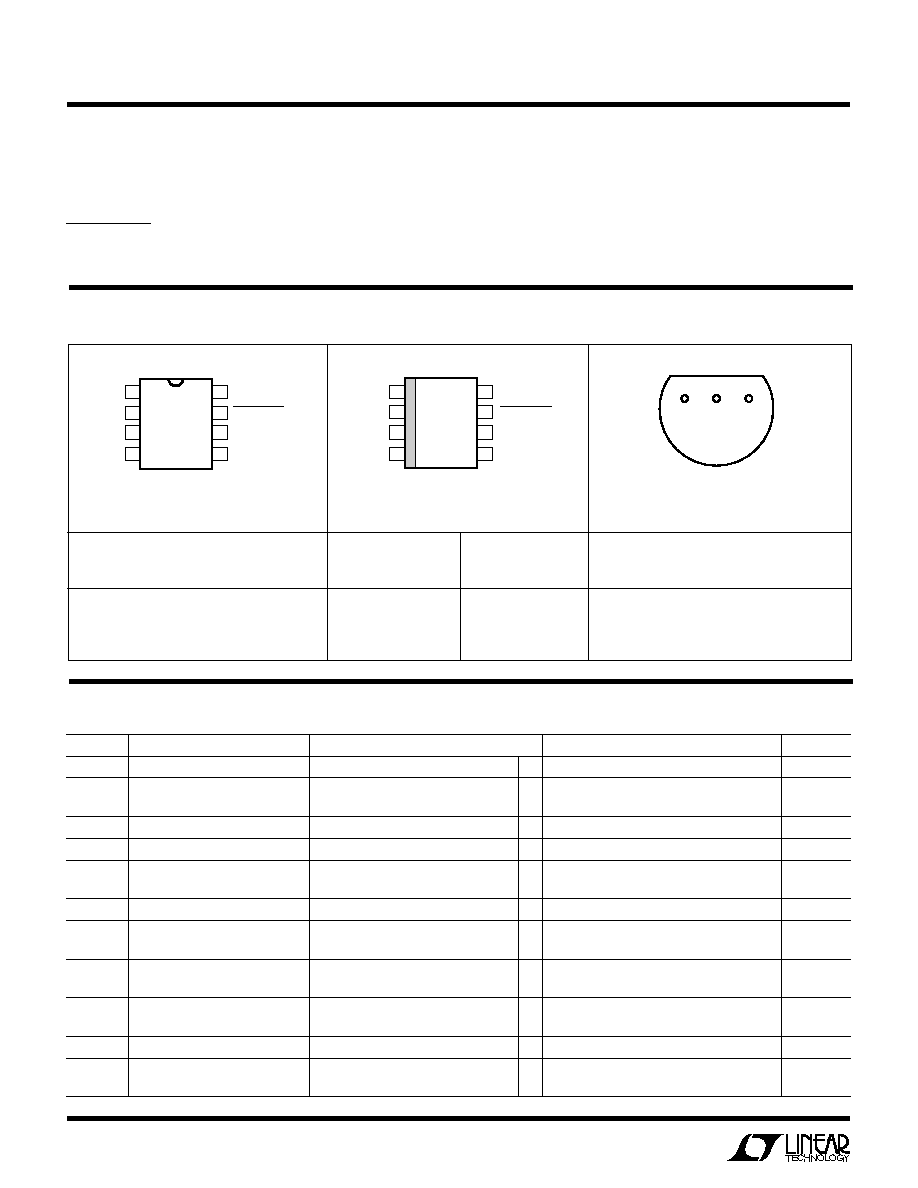
PACKAGE/ORDER I FOR ATIO
1
2
3
4
8
7
6
5
TOP VIEW
VIN
NC
SW
GND
SENSE
SHUTDOWN
NC
NC
N8 PACKAGE
8-LEAD PLASTIC DIP
LT1109 · PO102
1
2
3
4
8
7
6
5
TOP VIEW
SENSE
SHUTDOWN
NC
NC
V
IN
NC
SW
GND
S8 PACKAGE
8-LEAD PLASTIC SOIC
LT1109 · PO103
T
JMAX
= 100
°
C,
JA
= 130
°
C/W
T
JMAX
= 100
°
C,
JA
= 150
°
C/W
T
JMAX
= 100
°
C,
JA
= 160
°
C/W
GND
2
SW
3
1
Z PACKAGE
3-LEAD TO-92 PLASTIC
BOTTOM VIEW
OUT
V
LT1109 · POI01
LT1109CZ-5
LT1109CZ-12
ORDER PART
NUMBER
ORDER PART
NUMBER
S8 PART
MARKING
ORDER PART
NUMBER
LT1109CS8
LT1109CS8-5
LT1109CS8-12
LT1109CN8
LT1109CN8-5
LT1109CN8-12
1109
10905
10912
Operating Temperature Range ..................... 0
°
C to 70
°
C
Storage Temperature Range ................. 65
°
C to 150
°
C
Lead Temperature (Soldering, 10 sec.)................. 300
°
C
Switch Current ........................................................ 1.2A
A
U
G
W
A
W
U
W
A
R
BSOLUTE
XI
TI
S
(Voltages Referred to GND Pin)
Supply Voltage (V
OUT
) .............................. 0.4V to 20V
SW Pin Voltage .......................................... 0.4V to 50V
SHUTDOWN Pin Voltage ......................................... 6.0V
Maximum Power Dissipation ............................. 300mW
LT1109
3
C
C
HARA TERISTICS
U
W
A
TYPICAL PERFOR
CE
SYMBOL
PARAMETER
CONDITIONS
MIN
TYP
MAX
UNITS
Switch Leakage Current
V
SW
= 12V
1
10
µ
A
V
IH
SHUTDOWN Pin High
N8, S8 Package
q
2.0
V
V
IL
SHUTDOWN Pin Low
N8, S8 Package
q
0.8
V
I
IH
SHUTDOWN Pin Input Current
N8, S8 Package, V
SHUTDOWN
= 4V
q
10
µ
A
I
IL
SHUTDOWN Pin Input Current
N8, S8 Package, V
SHUTDOWN
= 0V
q
20
µ
A
The
q
denotes the specifications which apply over the full operating
temperature range.
ELECTRICAL C
C
HARA TERISTICS
T
A
= 25
°
C, V
IN
= 3V (LT1109CN8, LT1109CS8), unless otherwise specified.
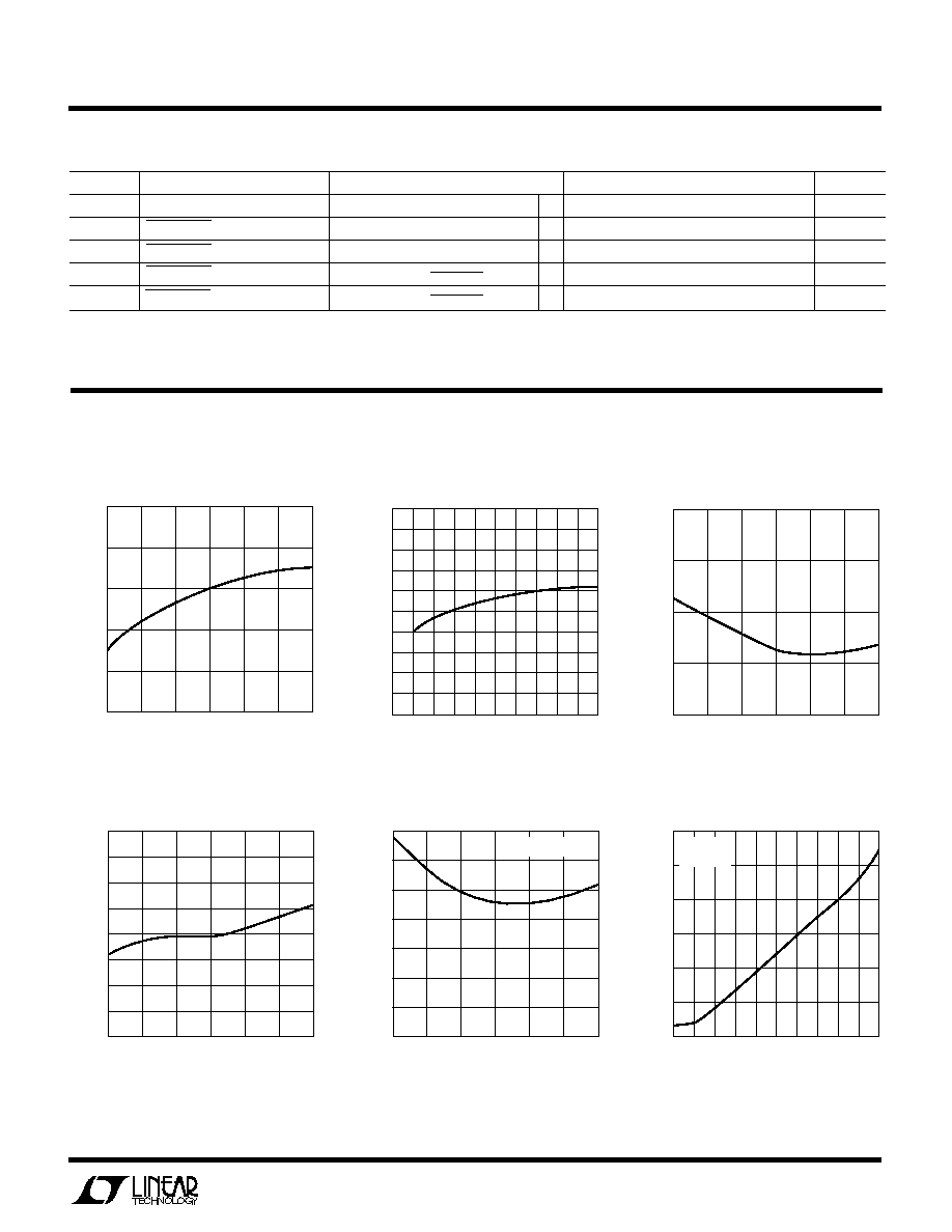
INPUT VOLTAGE (V)
0
110
OSCILLATOR FREQUENCY (kHz) 114
118
122
128
130
2
20
LT1109 · TPC03
4
6
8
10
126
124
120
116
112
12 14 16 18
TEMPERATURE (°C)
50
60
FREQUENCY (kHz)
80
100
120
140
160
25
100
LT1109 · TPC02
0
25
50
75
Oscillator Frequency
Oscillator Frequency
Switch ON Time
TEMPERATURE (°C)
50
3
SWITCH ON TIME (
µ
s)
4
7
100
LT1109 · TPC04
25
0
25
6
5
50
75
TEMPERATURE (°C)
50
0
V
CESAT
(mV)
200
700
100
LT1109 · TPC06
25
0
25
500
400
50
75
600
300
100
I
SW
= 500mA
SWITCH CURRENT (A)
0
0
V
CESAT
(V)
0.4
1.2
1.0
LT1109 · TPC07
0.1
0.3
0.5
0.8
0.6
0.7
0.9
1.0
0.2
V
IN
= 5V
T
A
= 25°C
0.2
0.4
0.6
0.8
Duty Cycle
Switch Saturation Voltage
Switch Saturation Voltage
TEMPERATURE (°C)
50
30
DUTY CYCLE (%)
40
70
100
LT1109 · TPC05
25
0
25
60
50
50
75
65
55
45
35
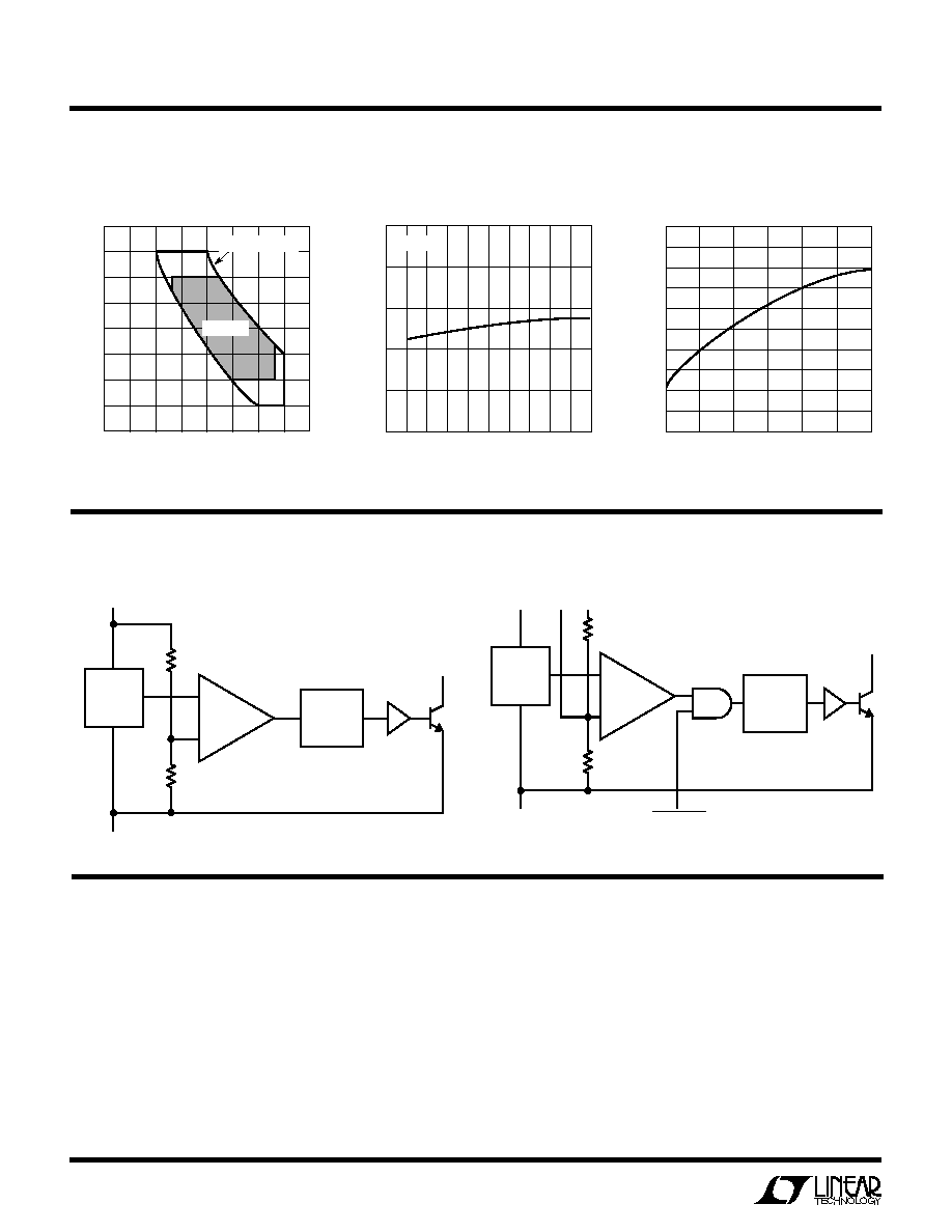
LT1109
4
W
I
D AGRA
BLOCK
S
LT1109-5, -12 Z Package
The LT1109Z-5 and LT1109Z-12 are fixed output voltage
step-up DC/DC converters in a 3-pin TO-92 package.
Power for internal regulator circuitry is taken from the
V
OUT
pin, a technique known as "bootstrapping." Circuit
operation can be best understood by referring to the block
diagram. V
OUT
, attenuated by R1 and R2, is applied to the
negative input of comparator A1. When this voltage falls
below the 1.25V reference voltage, the oscillator is turned
on and the power switch Q1 cycles at the oscillator
frequency of 120kHz. Switch cycling alternately builds
current in the inductor, then dumps it into the output
capacitor, increasing the output voltage. When A1's nega-
tive input rises above 1.25V, it turns off the oscillator. A
small amount of hysteresis in A1 obviates the need for
frequency compensation circuitry. When Q1 is off, current
into the V
OUT
pin drops to just 320
µ
A. Quiescent current
from the battery will be higher because the device oper-
ates off the
stepped-up voltage.
LT1109-5, -12 N8, S8 Package
C
C
HARA TERISTICS
U
W
A
TYPICAL PERFOR
CE
LT1109Z
U
ATIO
OPER
Minimum/Maximum
Oscillator Frequency vs t
ON
Quiescent Current
Quiescent Current
INPUT VOLTAGE (V)
0
200
QUIESCENT CURRENT (
µ
A)
300
450
20
LT1109 · TPC09
2
10
400
18
250
4
8
12 14
350
T
A
= 25°C
6
16
TEMPERATURE (°C)
50
200
QUIESCENT CURRENT (
µ
A)
280
400
100
LT1109 · TPC10
25
360
75
220
25
0
50
320
240
260
300
340
380
IN
V
LT1109 · TA04
GND
1.25V
REFERENCE
A1
DRIVER
SW
120kHz
OSCILLATOR
COMPARATOR
R2
250k
R1
+
SENSE
SHUTDOWN
Q1
FB
ON FIXED VERSION PIN 8 IS SENSE
ON ADJUSTABLE VERSION PIN 8 IS FB AND R1 AND R2 ARE DISCONNECTED
OUT
V
LT1109 · TA03
GND
1.25V
REFERENCE
A1
DRIVER
SW
120kHz
OSCILLATOR
COMPARATOR
R2
250k
R1
+
Q1
LT1109-5: R1 = 83k
LT1109-12: R1 = 29k
T
ON
(
µ
s)
2.0
80
OSCILLATOR FREQUENCY (kHz)
110
160
6.0
LT1109 · TPC08
2.5
4.0
140
120
5.5
150
90
3.0
3.5
4.5
5.0
130
100
T
A
= 25
°
C
0
°
C
T
A
70
°
C

LT1109
5
LT1109 S8 A D 8
U
ATIO
OPER
U
U
reduced by using the 8-pin version since the quiescent
current flows from a lower voltage source. The SHUT-
DOWN pin disables the oscillator when taken to a logic "0."
If left floating or tied high, the converter operates nor-
mally. With SHUTDOWN low, quiescent current remains
at 320
µ
A.
The 8-pin versions of the LT1109 have separate pins for
V
IN
and SENSE or FB and also have a SHUTDOWN pin.
Separating the device V
IN
pin from the SENSE pin allows
the device to be powered from the (lower) input voltage
rather than the (higher) output voltage. Although quies-
cent
current remains constant, quiescent power will be
U
S
A
O
PPLICATI
W
U
U
I FOR ATIO
Inductor Selection
A DC/DC converter operates by storing energy as mag-
netic flux in an inductor core, and then switching this
energy into the load. To operate as an efficient energy
transfer element, the inductor must fulfill three require-
ments. First, the inductance must be low enough for the
inductor to store adequate energy under the worst case
condition of minimum input voltage and switch-ON time.
The inductance must also be high enough so that maxi-
mum current ratings of the LT1109 and inductor are not
exceeded at the other worst case condition of maximum
input voltage and ON time. Additionally, the inductor core
must be able to store the required flux; i.e., it must not
saturate. At power levels generally encountered with
LT1109 designs, small ferrite surface-mount inductors
will function well. Lastly, the inductor must have suffi-
ciently low DC resistance so that excessive power is not
lost as heat in the windings. Look for DCR values in the
inductors' specification tables; values under 0.5
will give
best efficiency. An additional consideration is Electro-
Magnetic Interference (EMI). Toroid and pot core type
inductors are recommended in applications where EMI
must be kept to a minimum; for example, where there are
sensitive analog circuitry or transducers nearby. Rod core
types are a less expensive choice where EMI is not a
problem.
Specifying a proper inductor for an application requires
first establishing minimum and maximum input voltage,
output voltage, and output current. In a step-up converter,
the inductive events add to the input voltage to produce the
output voltage. Power required from the inductor is deter-
mined by
P
L
= (V
OUT
+ V
D
V
IN
) (I
OUT
)
(01)
P
F
L
OSC
02
( )
I
t
V
L
t
L
IN
( )
=
( )
04
E
LI
L
PEAK
=
( )
1
2
05
2
I
t
V
R
e
L
IN
R t
L
( )
=
( )
'
'
1
03
where V
D
is the diode drop (0.5V for a 1N5818 Schottky).
Energy required by the inductor per cycle must be equal or
greater than
in order for the converter to regulate the output.
When the switch is closed, current in the inductor builds
according to
where R' is the sum of the switch equivalent resistance
(0.8 typical at 25
°
C) and the inductor DC resistance. When
the drop across the switch is small compared to V
IN
, the
simple lossless equation
can be used. These equations assume that at t = 0,
inductor current is zero. This situation is called "discon-
tinuous mode operation" in switching regulator parlance.
Setting "t" to the switch-ON time from the LT1109 speci-
fication table (typically 4.2
µ
s) will yield I
PEAK
for a specific
"L" and V
IN
. Once I
PEAK
is known, energy in the inductor
at the end of the switch-ON time can be calculated as
E
L
must be greater than P
L
/F
OSC
for the converter to deliver
the required power. For best efficiency I
PEAK
should be