LT1110
1
D
U
ESCRIPTIO
The LT1110 is a versatile micropower DC-DC converter.
The device requires only three external components to
deliver a fixed output of 5V or 12V. The very low minimum
supply voltage of 1.0V allows the use of the LT1110 in
applications where the primary power source is a single
cell. An on-chip auxiliary gain block can function as a low
battery detector or linear post regulator.
The 70kHz oscillator allows the use of surface mount
inductors and capacitors in many applications. Quiescent
current is just 300
µ
A, making the device ideal in remote or
battery powered applications where current consumption
must be kept to a minimum.
The device can easily be configured as a step-up or
step-down converter, although for most step-down
applications or input sources greater than 3V, the LT1111
is recommended. Switch current limiting is user-adjustable
by adding a single external resistor. Unique reverse battery
protection circuitry limits reverse current to safe, non-
destructive levels at reverse supply voltages up to 1.6V.
S
FEATURE
s
Operates at Supply Voltages From 1.0V to 30V
s
Works in Step-Up or Step-Down Mode
s
Only Three External Off-the-Shelf Components
Required
s
Low-Battery Detector Comparator On-Chip
s
User-Adjustable Current Limit
s
Internal 1A Power Switch
s
Fixed or Adjustable Output Voltage Versions
s
Space-Saving 8-Pin MiniDIP or S8 Package
U
S
A
O
PPLICATI
s
Pagers
s
Cameras
s
Single-Cell to 5V Converters
s
Battery Backup Supplies
s
Laptop and Palmtop Computers
s
Cellular Telephones
s
Portable Instruments
s
Laser Diode Drivers
s
Hand-Held Inventory Computers
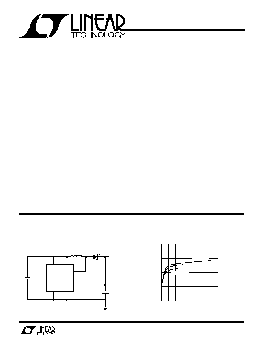
Micropower
DC-DC Converter
Adjustable and Fixed 5V, 12V
LOAD CURRENT (mA)
0
EFFICIENCY (%)
50
60
70
80
85
90
10
20
30
40
LT1110 ∑ TA02
75
65
55
5
15
25
35
V
IN
= 1.50V
V
IN
= 1.25V
V
IN
= 1.00V
U
A
O
PPLICATI
TYPICAL
Efficiency
All Surface Mount
Single Cell to 5V Converter
LT1110 ∑ TA01
+
GND
SW2
SENSE
SW1
LIM
I
IN
V
5
4
1
3
8
LT1110-5
1.5V
AA CELL*
*ADD 10 F DECOUPLING CAPACITOR IF BATTERY
IS MORE THAN 2" AWAY FROM LT1110.
µ
15
µ
F
TANTALUM
5V
MBRS120T3
SUMIDA
CD54-470K
47
µ
H
OPERATES WITH CELL VOLTAGE 1.0V
2
LT1110
2
W
U
U
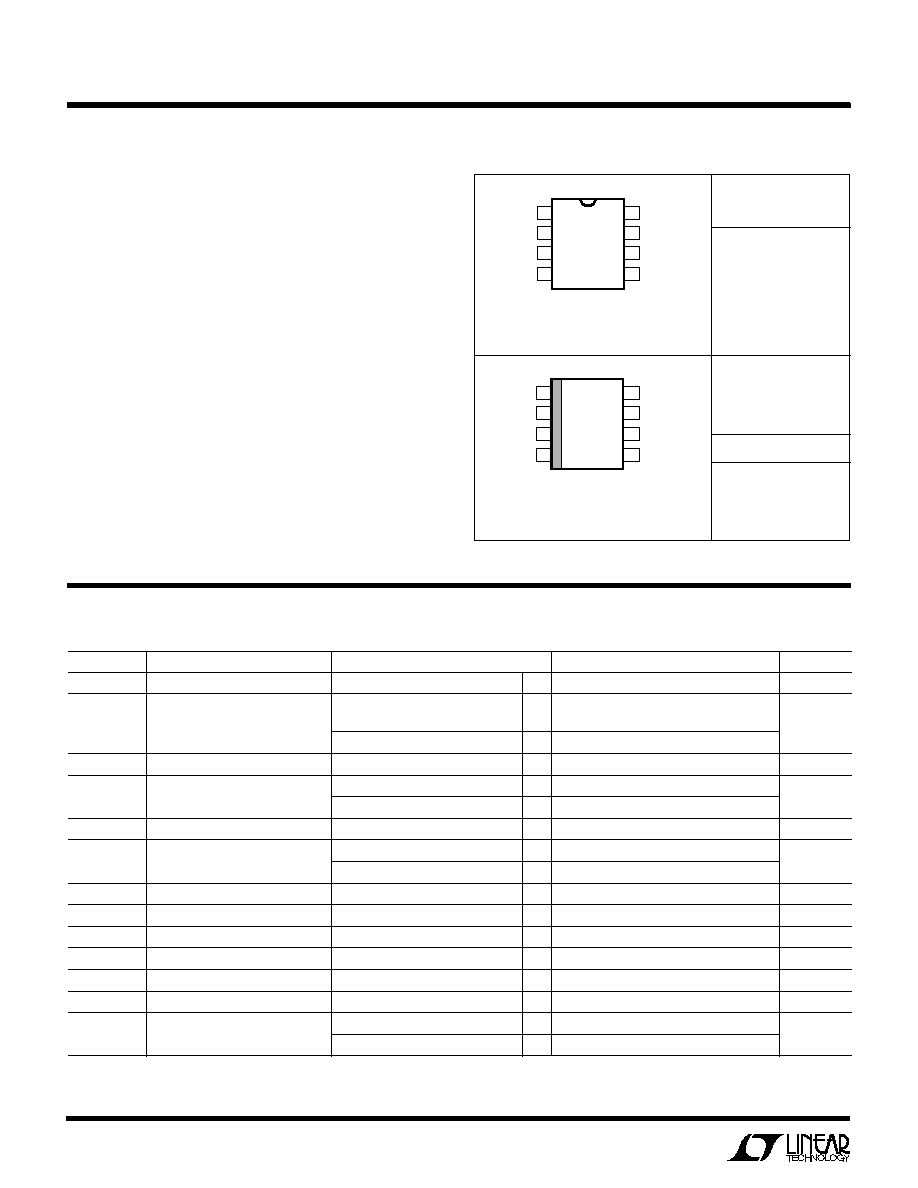
PACKAGE/ORDER I FOR ATIO
A
U
G
W
A
W
U
W
A
R
BSOLUTE
XI
TI
S
Supply Voltage, Step-Up Mode ................................ 15V
Supply Voltage, Step-Down Mode ........................... 36V
SW1 Pin Voltage ...................................................... 50V
SW2 Pin Voltage ......................................... ≠ 0.5V to V
IN
Feedback Pin Voltage (LT1110) .............................. 5.5V
Switch Current ........................................................ 1.5A
Maximum Power Dissipation ............................. 500mW
Operating Temperature Range ..................... 0
∞
C to 70
∞
C
Storage Temperature Range .................. ≠65
∞
C to 150
∞
C
Lead Temperature (Soldering, 10 sec.)................. 300
∞
C
ORDER PART
NUMBER
LT1110CN8
LT1110CN8-5
LT1110CN8-12
1110
11105
11012
Consult factory for Industrial and Military grade parts.
T
JMAX
= 90
∞
C,
JA
= 150
∞
C/W
1
2
3
4
8
7
6
5
TOP VIEW
I
LIM
V
IN
SW1
SW2
FB (SENSE)*
SET
A0
GND
N8 PACKAGE
8-LEAD PLASTIC DIP
*FIXED VERSIONS
T
JMAX
= 90
∞
C,
JA
= 130
∞
C/W
1
2
3
4
8
7
6
5
TOP VIEW
FB (SENSE)*
SET
A0
GND
I
LIM
V
IN
SW1
SW2
S8 PACKAGE
8-LEAD PLASTIC SOIC
*FIXED VERSIONS
SYMBOL
PARAMETER
CONDITIONS
MIN
TYP
MAX
UNITS
I
Q
Quiescent Current
Switch Off
q
300
µ
A
V
IN
Input Voltage
Step-Up Mode
q
1.15
12.6
V
1.0
12.6
V
Step-Down Mode
q
30
V
Comparator Trip Point Voltage
LT1110 (Note 1)
q
210
220
230
mV
V
OUT
Output Sense Voltage
LT1110-5 (Note 2)
q
4.75
5.00
5.25
V
LT1110-12 (Note 2)
q
11.4
12.00
12.6
V
Comparator Hysteresis
LT1110
q
4
8
mV
Output Hysteresis
LT1110-5
q
90
180
mV
LT1110-12
q
200
400
mV
f
OSC
Oscillator Frequency
q
52
70
90
kHz
DC
Duty Cycle
Full Load (V
FB
<
V
REF
)
q
62
69
78
%
t
ON
Switch ON Time
q
7.5
10
12.5
µ
s
I
FB
Feedback Pin Bias Current
LT1110, V
FB
= 0V
q
70
150
nA
I
SET
Set Pin Bias Current
V
SET
= V
REF
q
100
300
nA
V
AO
AO Output Low
I
AO
=
≠300
µ
A, V
SET
= 150mV
q
0.15
0.4
V
Reference Line Regulation
1.0V
V
IN
1.5V
q
0.35
1.0
%/V
1.5V
V
IN
12V
q
0.05
0.1
%/V
ELECTRICAL C
C
HARA TERISTICS
T
A
= 25
∞
C, V
IN
= 1.5V, unless otherwise noted.
S8 PART MARKING
LT1110CS8
LT1110CS8-5
LT1110CS8-12
LT1110
3
V
CESAT
Switch Saturation Voltage
V
IN
= 1.5V, I
SW
= 400mA
300
400
mV
Step-Up Mode
q
600
mV
V
IN
= 1.5V, I
SW
= 500mA
400
550
mV
q
750
mV
V
IN
= 5V, I
SW
= 1A
700
1000
mV
A
V
A2 Error Amp Gain
R
L
= 100k
(Note 3)
q
1000
5000
V/V
I
REV
Reverse Battery Current
(Note 4)
750
mA
I
LIM
Current Limit
220
Between I
LIM
and V
IN
400
mA
Current Limit Temperature
≠ 0.3
%/
∞
C
Coefficient
I
LEAK
Switch OFF Leakage Current
Measured at SW1 Pin
1
10
µ
A
V
SW2
Maximum Excursion Below GND
I
SW1
10
µ
A, Switch Off
≠ 400
≠ 350
mV
ELECTRICAL C
C
HARA TERISTICS
T
A
= 25
∞
C, V
IN
= 1.5V, unless otherwise noted.
SYMBOL
PARAMETER
CONDITIONS
MIN
TYP
MAX
UNITS
Note 3: 100k
resistor connected between a 5V source and the AO pin.
Note 4: The LT1110 is guaranteed to withstand continuous application of
+1.6V applied to the GND and SW2 pins while V
IN
, I
LIM
, and SW1 pins are
grounded.
The
q
denotes the specifications which apply over the full operating
temperature range.
Note 1: This specification guarantees that both the high and low trip point
of the comparator fall within the 210mV to 230mV range.
Note 2: This specification guarantees that the output voltage of the fixed
versions will always fall within the specified range. The waveform at the
sense pin will exhibit a sawtooth shape due to the comparator hysteresis.
C
C
HARA TERISTICS
U
W
A
TYPICAL PERFOR
CE
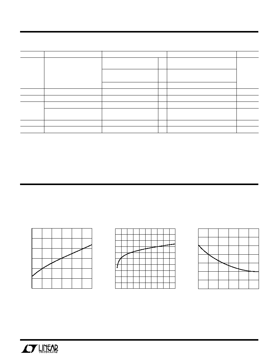
Oscillator Frequency
Oscillator Frequency
Switch On Time
INPUT VOLTAGE (V)
0
64
FREQUENCY (KHz)
66
70
72
74
78
80
3
6
9
12
LT1110 ∑ TPC02
15 18 21
62
60
24 27 30
68
76
TEMPERATURE (
∞
C)
ON TIME (
µ
s)
≠50
≠25
0
25
LT1110 ∑ TPC03
50
75
100
14
13
12
11
10
9
8
7
TEMPERATURE (
∞
C)
≠50
40
OSCILLATOR FREQUENCY (KHz)
50
60
70
80
90
100
≠25
0
25
50
LT1110 ∑ TPC01
75
100
LT1110
4
I
SWITCH
(A)
ON VOLTAGE (V)
0
0.2
0.4
0.6
LT1110 ∑ TPC07
0.8
1.0
1.4
1.2
1.0
0.8
0.6
0.4
0.2
0
V
IN
= 12V
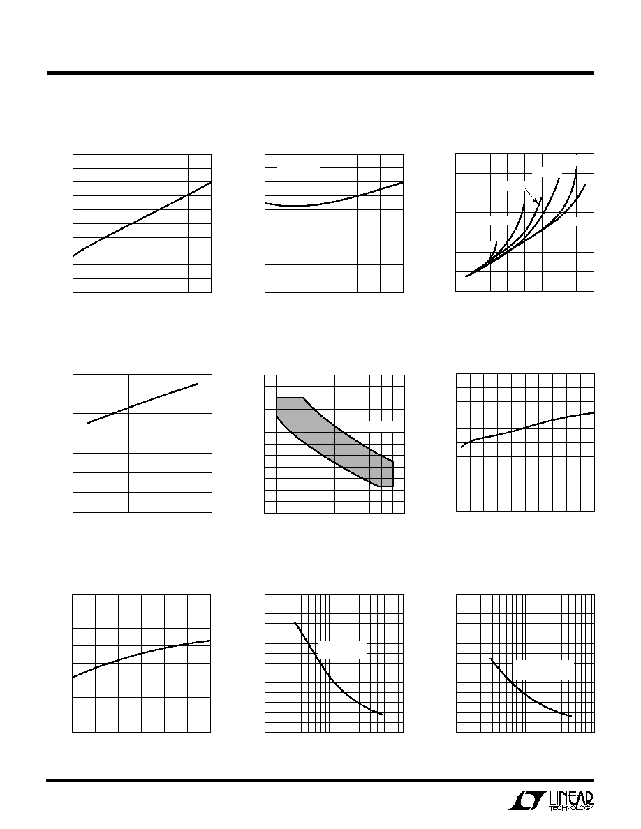
C
C
HARA TERISTICS
U
W
A
TYPICAL PERFOR
CE
Saturation Voltage
Duty Cycle
Switch Saturation Voltage
Step-Up Mode
Switch On Voltage
Minimum/Maximum Frequency vs
Step-Down Mode
On Time
Quiescent Current
Maximum Switch Current vs
Maximum Switch Current vs
Quiescent Current
R
LIM
Step-Up
R
LIM
Step-Down
TEMPERATURE (
∞
C)
DUTY CYCLE (%)
≠50
≠25
0
25
LT1110 ∑ TPC04
50
75
100
78
76
74
72
70
68
66
64
62
60
58
TEMPERATURE (
∞
C)
V
CESAT
(mV)
≠50
≠ 25
0
25
LT1110 ∑ TPC05
50
75
100
500
450
400
350
300
250
200
150
100
50
0
V
IN
= 1.5V
I
SW
= 500mA
I (A)
0
0
V (V)
0.2
0.4
0.6
1.2
1.4
0.2
0.4
0.8
1.2
LT1110 ∑ TPC06
1.0
1.4
1.6
SWITCH
CESAT
V
IN
= 1.0V
V = 1.2V
IN
V
IN
= 1.5V
V
IN
= 5.0V
V = 2.0V
IN
0.6
1.0
0.8
V
IN
= 3.0V
INPUT VOLTAGE (V)
QUIESCENT CURRENT (
µ
A)
0
LT1110 ∑ TPC09
3
400
380
360
340
320
280
260
6
240
220
200
300
9
12 15 18 21 24 27
30
TEMPERATURE (
∞
C)
QUIESCENT CURRENT (
µ
A)
≠50
LT1110 ∑ TPC10
500
450
400
350
250
≠25
150
100
200
300
0
25
50
75
100
R
LIM
(
)
SWITCH CURRENT (A)
10
LT1110 ∑ TPC11
100
1.5
1.3
1.1
0.9
1000
0.7
0.5
0.3
0.1
STEP-UP MODE
V
IN
5V
R
LIM
(
)
SWITCH CURRENT (A)
10
LT1110 ∑ TPC12
100
1.5
1.3
1.1
0.9
1000
0.7
0.5
0.3
0.1
STEP-DOWN MODE
V
IN
= 12V
SWITCH ON TIME (
µ
s)
OSCILLATOR FREQUENCY (KHz)
7
9
LT1110 ∑ TPC08
10
100
90
80
70
60
50
40
13
0
∞
C
T
A
70
∞
C
8
11
12
95
85
75
65
55
45
LT1110
5
W
I
D AGRA
BLOCK
LT1110
C
C
HARA TERISTICS
U
W
A
TYPICAL PERFOR
CE
Set Pin Bias Current
FB Pin Bias Current
Reference Voltage
I
LIM
(Pin 1): Connect this pin to V
IN
for normal use. Where
lower current limit is desired, connect a resistor between
I
LIM
and V
IN
. A 220
resistor will limit the switch current
to approximately 400mA.
V
IN
(Pin 2): Input supply voltage.
SW1 (Pin 3):
Collector of power transistor. For step-up
mode connect to inductor/diode. For step-down mode
connect to V
IN
.
SW2 (Pin 4):
Emitter of power transistor. For step-up
mode connect to ground. For step-down mode connect to
inductor/diode. This pin must never be allowed to go more
than a Schottky diode drop below ground.
GND (Pin 5): Ground.
AO (Pin 6): Auxiliary Gain Block (GB) output. Open collector,
can sink 300
µ
A.
SET (Pin 7): GB input. GB is an op amp with positive input
connected to SET pin and negative input connected to
220mV reference.
FB/SENSE (Pin 8): On the LT1110 (adjustable) this pin
goes to the comparator input. On the LT1110-5 and
LT1110-12, this pin goes to the internal application resistor
that sets output voltage.
PI
U
FU
U
C
U
S
O
TI
TEMPERATURE (
∞
C)
BIAS CURRENT (nA)
≠50
LT1110 ∑ TPC13
160
140
120
100
60
≠25
20
0
40
80
0
25
50
75
100
TEMPERATURE (
∞
C)
V
REF
(mV)
≠50
≠25
0
25
LT1110 ∑ TPC15
50
75
100
226
224
222
220
218
216
214
212
TEMPERATURE (
∞
C)
BIAS CURRENT (nA)
≠50
120
100
90
70
40
≠25
10
0
30
60
0
25
50
75
100
20
50
80
110
LT1110 ∑ TPC14
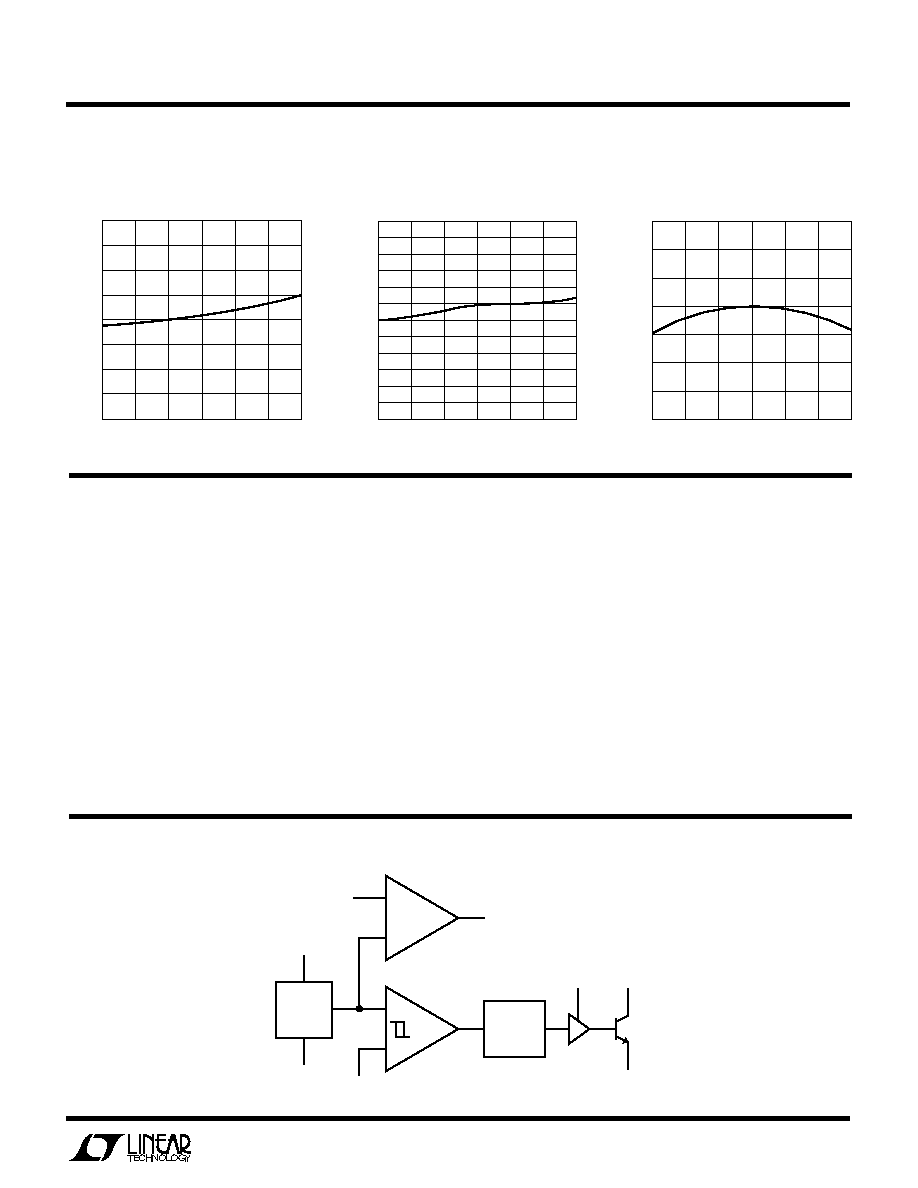
LT1110 ∑ BD01
IN
V
GND
SET
AO
GAIN BLOCK/ERROR AMP
220mV
REFERENCE
A1
A2
DRIVER
+
≠
FB
SW1
SW2
LIM
I
OSCILLATOR
COMPARATOR
Q1