1
LT1112/LT1114
D
U
ESCRIPTIO
S
FEATURE
Dual/Quad Low Power
Precision, Picoamp Input Op Amps
The LT1112 dual and LT1114 quad op amps achieve a new
standard in combining low cost and outstanding precision
specifications.
The performance of the selected prime grades matches or
exceeds competitive devices. In the design of the LT1112/
LT1114 however, particular emphasis has been placed on
optimizing performance in the low cost plastic and SO
packages. For example, the 75
µ
V maximum offset voltage
in these low cost packages is the lowest on any dual or
quad non-chopper op amp.
The LT1112/LT1114 also provide a full set of matching
specifications, facilitating their use in such matching
dependent applications as two and three op amp instru-
mentation amplifiers.
Another set of specifications is furnished at
±
1V supplies.
This, combined with the low 320
µ
A supply current per
amplifier, allows the LT1112/LT1114 to be powered by
two nearly discharged AA cells.
s
S8 Package ≠ Standard Pinout
s
Offset Voltage ≠ Prime Grade: 60
µ
V Max
s
Offset Voltage ≠ Low Cost Grade
(Including Surface Mount Dual/Quad): 75
µ
V Max
s
Offset Voltage Drift: 0.5
µ
V/
∞
C Max
s
Input Bias Current: 250pA Max
s
0.1Hz to 10Hz Noise: 0.3
µ
V
P-P
, 2.2pA
P-P
s
Supply Current per Amplifier: 400
µ
A Max
s
CMRR: 120dB Min
s
Voltage Gain: 1 Million Min
s
Guaranteed Specs with
±
1.0V Supplies
s
Guaranteed Matching Specifications
s
LT1114 in Narrow Surface Mount Package
U
S
A
O
PPLICATI
s
Picoampere/Microvolt Instrumentation
s
Two and Three Op Amp Instrumentation Amplifers
s
Thermocouple and Bridge Amplifiers
s
Low Frequency Active Filters
s
Photo Current Amplifiers
s
Battery-Powered Systems
Protected by U.S. Patents 4,575,685; 4,775,884 and 4,837,496
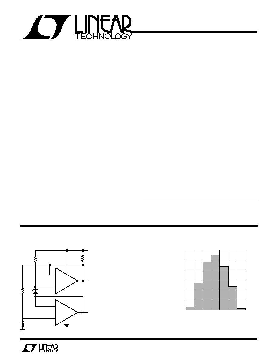
Distribution of Input Offset Voltage
(In All Packages)
INPUT OFFSET VOLTAGE (
µ
V)
≠70
PERCENT OF UNITS
20
25
30
≠10
30
15
10
≠50
≠30
10
50
70
5
0
V
S
= ±15V
T
A
= 25∞C
LT1112/14 ∑ TA02
≠
+
1/2 LT1112
≠
+
1/2 LT1112
LT1004-1.2
75k
0.1%
46.4k
0.1%
2
3
6
5
4
7
8
1
0.765V
R
X
15k
3V
2.000V
LT1112/14 ∑ TA01
TOTAL SUPPLY CURRENT = 700
µ
A
2V REFERENCE: SOURCES 1.7mA, SINKS 5mA
OPTIONAL R
X
= 300
INCREASES SOURCE
CURRENT TO 5mA
0.765V REFERENCE: SOURCES 5mA,
SINKS 0.5mA
TEMPERATURE COEFFICIENT LIMITED
BY REFERENCE = 20ppm/∞C
MINIMUM SUPPLY = 2.7V
Dual Output, Buffered Reference (On Single 3V Supply)
2
LT1112/LT1114
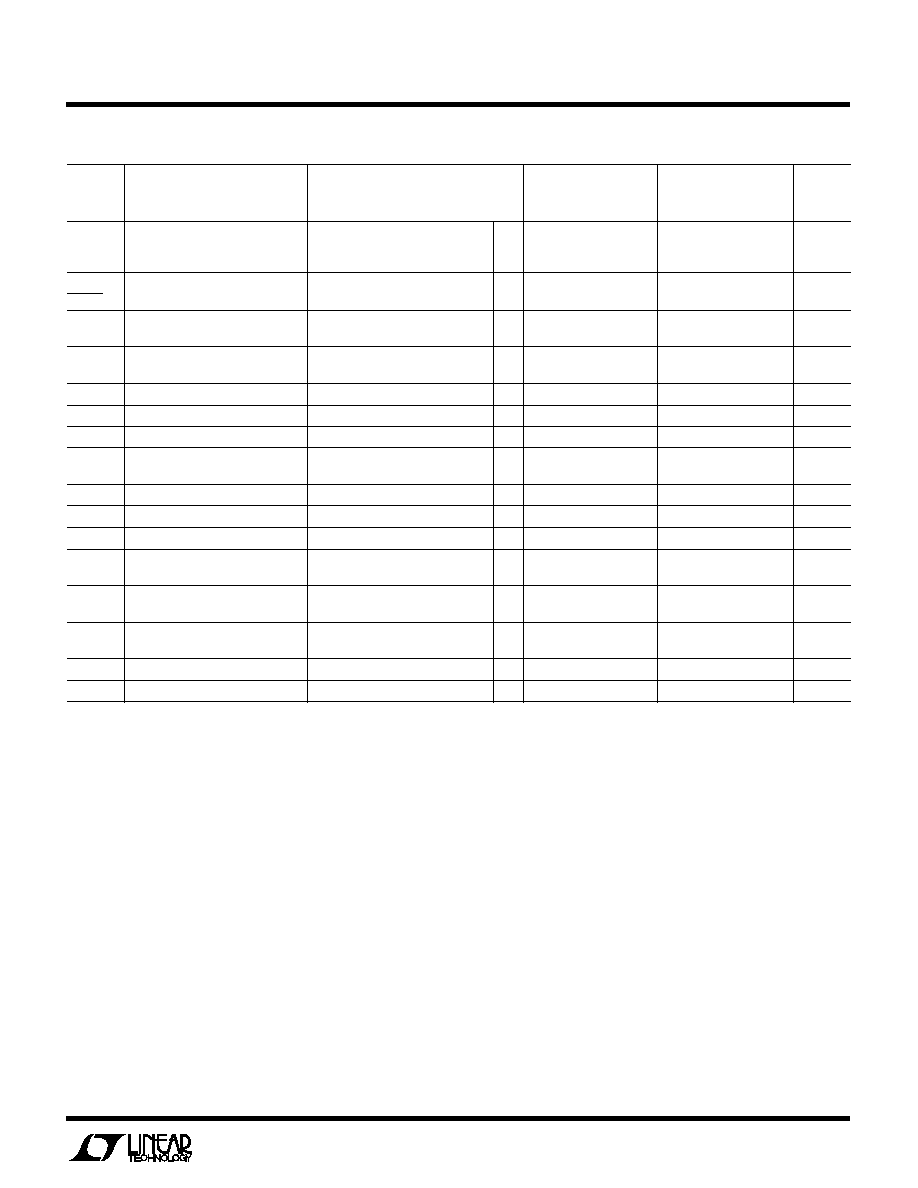
SYMBOL PARAMETER
CONDITIONS (Note 2)
MIN
TYP
MAX
MIN
TYP
MAX
UNITS
V
OS
Input Offset Voltage
20
60
25
75
µ
V
V
S
=
±
1.0V
40
110
45
130
µ
V
V
OS
Long Term Input Offset
0.3
0.3
µ
V/Mo
Time
Voltage Stability
I
OS
Input Offset Current
50
180
60
230
pA
LT1114S
75
330
pA
I
B
Input Bias Current
±
70
±
250
±
80
±
280
pA
LT1114S
±
100
±
450
pA
e
n
Input Noise Voltage
0.1Hz to 10Hz (Note 9)
0.3
0.9
0.3
0.9
µ
V
P-P
A
U
G
W
A
W
U
W
A
R
BSOLUTE
XI
TI
S
Supply Voltage .....................................................
±
20V
Differential Input Current (Note 1) .....................
±
10mA
Input Voltage (Equal to Supply Voltage) ...............
±
20V
Output Short-Circuit Duration ......................... Indefinite
Storage Temperature Range ................ ≠ 65
∞
C to 150
∞
C
Lead Temperature (Soldering, 10 sec)................ 300
∞
C
ORDER PART
NUMBER
ORDER PART
NUMBER
PART MARKING
Operating Temperature Range
LT1112AM/LT1112M
LT1114AM/LT1114M ...................... ≠ 55
∞
C to 125
∞
C
LT1112AC/LT1112C/LT1112S8
LT1114AC/LT1114C/LT1114S .......... ≠ 40
∞
C to 85
∞
C
T
JMAX
= 140
∞
C,
JA
= 190
∞
C/W
LT1112S8
LT1112AMJ8
LT1112MJ8
LT1112ACN8
LT1112CN8
1112
ORDER PART
NUMBER
ORDER PART
NUMBER
LT1114S
LT1114AMJ
LT1114MJ
LT1114ACN
LT1114CN
T
JMAX
= 160
∞
C,
JA
= 80
∞
C/W (J)
T
JMAX
= 140
∞
C,
JA
= 110
∞
C/W (N)
T
JMAX
= 160
∞
C,
JA
= 100
∞
C/W (J8)
T
JMAX
= 140
∞
C,
JA
= 130
∞
C/W (N8)
W
U
U
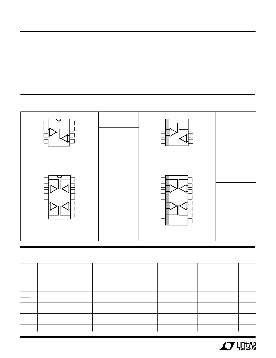
PACKAGE/ORDER I FOR ATIO
ELECTRICAL CHARACTERISTICS
V
S
=
±
15V, V
CM
= 0V, T
A
= 25
∞
C, unless otherwise noted.
LT1112AM/AC
LT1114AM/AC
LT1112M/C/S8
LT1114M/C/S
T
JMAX
= 140
∞
C,
JA
= 150
∞
C/W
TOP VIEW
OUT A
≠IN A
+IN A
V
≠
V
+
OUT B
≠IN B
+IN B
N8 PACKAGE
8-LEAD PLASTIC DIP
J8 PACKAGE
8-LEAD CERAMIC DIP
1
2
3
4
8
7
6
5
A
B
1
2
3
4
5
6
7
TOP VIEW
J PACKAGE
14-LEAD CERAMIC DIP
N PACKAGE
14-LEAD PLASTIC DIP
14
13
12
11
10
9
8
OUT A
≠IN A
+IN A
V
+
+IN B
≠IN B
OUT B
OUT D
≠IN D
+IN D
V
≠
+IN C
≠IN C
OUT C
A
D
B
C
1
2
3
4
8
7
6
5
TOP VIEW
V
+
OUT B
≠IN B
+IN B
OUT A
≠IN A
+IN A
V
≠
S8 PACKAGE
8-LEAD PLASTIC SO
B
A
TOP VIEW
S PACKAGE
16-LEAD PLASTIC SO (NARROW)
1
2
3
4
5
6
7
8
16
15
14
13
12
11
10
9
OUT A
≠IN A
+IN A
V
+
+IN B
≠IN B
OUT B
NC
OUT D
≠IN D
+IN D
V
≠
+IN C
≠IN C
OUT C
NC
A
D
B
C
3
LT1112/LT1114
SYMBOL PARAMETER
CONDITIONS (Note 2)
MIN
TYP
MAX
MIN
TYP
MAX
UNITS
Input Noise Voltage Density
f
O
= 10Hz (Note 9)
16
28
16
28
nV/
Hz
f
O
= 1000Hz (Note 9)
14
18
14
18
nV/
Hz
i
n
Input Noise Current
0.1Hz to 10Hz
2.2
2.2
pA
P-P
Input Noise Current Density
f
O
= 10Hz
0.030
0.030
pA/
Hz
f
O
= 1000Hz
0.008
0.008
pA/
Hz
V
CM
Input Voltage Range
±
13.5
±
14.3
±
13.5
±
14.3
V
CMRR
Common-Mode Rejection Ratio
V
CM
=
±
13.5V
120
136
115
136
dB
PSRR
Power Supply Rejection Ratio
V
S
=
±
1.0V to
±
20V
116
126
114
126
dB
Minimum Supply Voltage
(Note 4)
±
1.0
±
1.0
V
R
IN
Input Resistance
Differential Mode
(Note 3)
20
50
15
40
M
Common Mode
800
700
G
A
VOL
Large-Signal Voltage Gain
V
O
=
±
12V, R
L
= 10k
1000
5000
800
5000
V/mV
V
O
=
±
10V, R
L
= 2k
800
1500
600
1300
V/mV
V
OUT
Output Voltage Swing
R
L
= 10k
±
13.0
±
14.0
±
13.0
±
14.0
V
R
L
= 2k
±
11.0
±
12.4
±
11.0
±
12.4
V
SR
Slew Rate
0.16
0.30
0.16
0.30
V/
µ
s
GBW
Gain-Bandwidth Product
f
O
= 10kHz
450
750
450
750
kHz
I
S
Supply Current per Amplifier
350
400
350
450
µ
A
V
S
=
±
1.0V
320
370
320
420
µ
A
Channel Separation
f
O
= 10Hz
150
150
dB
V
OS
Offset Voltage Match
(Note 5)
35
100
40
130
µ
V
I
B
+
Noninverting Bias Current Match
100
450
100
500
pA
(Notes 5, 6)
LT1114S
120
680
pA
CMRR
Common-Mode Rejection Match
(Notes 5, 7)
117
136
113
136
dB
PSRR
Power Supply Rejection Match
(Notes 5, 7)
114
130
112
130
dB
ELECTRICAL CHARACTERISTICS
V
S
=
±
15V, V
CM
= 0V, T
A
= 25
∞
C, unless otherwise noted.
LT1112AM/AC
LT1114AM/AC
LT1112M/C/S8
LT1114M/C/S
SYMBOL PARAMETER
CONDITIONS (Note 2)
MIN
TYP
MAX
MIN
TYP
MAX
UNITS
V
OS
Input Offset Voltage
q
35
120
45
150
µ
V
V
S
=
±
1.2V
q
60
220
70
260
µ
V
V
OS
Average Input Offset Voltage Drift
(Note 8)
q
0.15
0.5
0.20
0.75
µ
V/
∞
C
Temp
I
OS
Input Offset Current
q
80
400
100
500
pA
I
B
Input Bias Current
q
±
150
±
600
±
170
±
700
pA
V
CM
Input Voltage Range
q
±
13.5
±
14.1
±
13.5
±
14.1
V
CMRR
Common-Mode Rejection Ratio
V
CM
=
±
13.5V
q
116
130
111
130
dB
PSRR
Power Supply Rejection Ratio
V
S
=
±
1.2V to
±
20V
q
112
124
110
124
dB
A
VOL
Large-Signal Voltage Gain
V
O
=
±
12V, R
L
= 10k
q
500
2500
400
2500
V/mV
V
O
=
±
10V, R
L
= 2k
q
200
600
170
500
V/mV
ELECTRICAL CHARACTERISTICS
V
S
=
±
15V, ≠ 55
∞
C
T
A
125
∞
C, unless otherwise noted.
LT1112AMJ8
LT1114AMJ
LT1112MJ8
LT1114MJ
4
LT1112/LT1114
SYMBOL PARAMETER
CONDITIONS (Note 2)
MIN
TYP
MAX
MIN
TYP
MAX
UNITS
V
OUT
Output Voltage Swing
R
L
= 10k
q
±
13.0
±
13.85
±
13.0
±
13.85
V
SR
Slew Rate
q
0.12
0.22
0.12
0.22
V/
µ
s
I
S
Supply Current per Amplifier
q
380
460
380
530
µ
A
V
OS
Offset Voltage Match
(Note 5)
q
55
200
70
240
µ
V
Offset Voltage Match Drift
(Notes 5, 8)
q
0.2
0.7
0.3
1.0
µ
V/
∞
C
I
B
+
Noninverting Bias Current Match
(Notes 5, 6)
q
150
750
170
850
pA
CMRR
Common-Mode Rejection Ratio
(Notes 5, 7)
q
112
130
106
130
dB
PSRR
Power Supply Rejection Ratio
(Notes 5, 7)
q
109
126
106
126
dB
ELECTRICAL CHARACTERISTICS
V
S
=
±
15V, ≠ 55
∞
C
T
A
125
∞
C, unless otherwise noted.
SYMBOL PARAMETER
CONDITIONS (Note 2)
MIN
TYP
MAX
MIN
TYP
MAX
UNITS
V
OS
Input Offset Voltage
LT1112N8
q
27
100
30
125
µ
V
LT1112S8, LT1114N/S
q
35
125
45
150
µ
V
V
S
=
±
1.2V
q
50
175
65
210
µ
V
V
OS
Average Input Offset Voltage Drift
LT1112N8
q
0.15
0.5
0.2
0.75
µ
V/
∞
C
Temp
(Note 8)
LT1112S8, LT1114N/S
q
0.3
1.1
0.4
1.3
µ
V/
∞
C
I
OS
Input Offset Current
q
60
220
70
290
pA
LT1114S
q
90
420
pA
I
B
Input Bias Current
q
±
80
±
300
±
90
±
350
pA
LT1114S
q
±
115
±
550
pA
V
CM
Input Voltage Range
q
±
13.5
±
14.2
±
13.5
±
14.2
V
CMRR
Common-Mode Rejection Ratio
V
CM
=
±
13.5V
q
118
133
113
133
dB
PSRR
Power Supply Rejection Ratio
V
S
=
±
1.2V to
±
20V
q
114
125
112
125
dB
A
VOL
Large-Signal Voltage Gain
V
O
=
±
12V, R
L
= 10k
q
800
4000
650
4000
V/mV
V
O
=
±
10V, R
L
= 2k
q
500
1300
400
1000
V/mV
V
OUT
Output Voltage Swing
R
L
= 10k
q
±
13.0
±
13.9
±
13.0
±
13.9
V
SR
Slew Rate
q
0.14
0.27
0.14
0.27
V/
µ
s
I
S
Supply Current per Amplifier
q
370
440
370
500
µ
A
V
OS
Offset Voltage Match
LT1112N8
q
45
170
55
210
µ
V
(Note 5)
LT1112S8, LT1114N/S
q
55
220
70
270
µ
V
Offset Voltage Match Drift
LT1112N8
q
0.2
0.7
0.3
1.0
µ
V/
∞
C
(Notes 5, 8)
LT1112S8, LT1114N/S
q
0.4
1.6
0.5
1.9
µ
V/
∞
C
I
B
+
Noninverting Bias Current Match
q
120
530
135
620
pA
(Notes 5, 6)
LT1114S
q
160
880
pA
CMRR
Common-Mode Rejection Ratio
(Notes 5, 7)
q
114
134
109
134
dB
PSRR
Power Supply Rejection Ratio
(Notes 5, 7)
q
110
128
108
128
dB
ELECTRICAL CHARACTERISTICS
V
S
=
±
15V, 0
∞
C
T
A
70
∞
C, unless otherwise noted.
LT1112ACN8
LT1114ACN
LT1112N8/S8
LT1114CN/S
LT1112AMJ8
LT1114AMJ
LT1112MJ8
LT1114MJ
5
LT1112/LT1114
SYMBOL PARAMETER
CONDITIONS (Note 2)
MIN
TYP
MAX
MIN
TYP
MAX
UNITS
V
OS
Input Offset Voltage
LT1112N8
q
30
110
35
135
µ
V
LT1112S8, LT1114N/S
q
40
135
45
160
µ
V
V
S
=
±
1.2V
q
55
200
60
240
µ
V
V
OS
Average Input Offset Voltage Drift
LT1112N8
q
0.15
0.50
0.20
0.75
µ
V/
∞
C
Temp
LT1112S8, LT1114N/S
q
0.30
1.10
0.40
1.30
µ
V/
∞
C
I
OS
Input Offset Current
q
70
330
85
400
pA
LT1114S
q
110
600
pA
I
B
Input Bias Current
q
±
110
±
500
±
120
±
550
pA
LT1114S
q
±
150
±
800
pA
V
CM
Input Voltage Range
q
±
13.5
±
14.1
±
13.5
±
14.1
V
CMRR
Common-Mode Rejection Ratio
V
CM
=
±
13.5V
q
117
132
112
132
dB
PSRR
Power Supply Rejection Ratio
V
S
=
±
1.2V to
±
20V
q
113
125
111
125
dB
A
VOL
Large-Signal Voltage Gain
V
O
=
±
12V, R
L
= 10k
q
700
3300
600
3300
V/mV
V
O
=
±
10V, R
L
= 2k
q
400
1100
300
900
V/mV
V
OUT
Output Voltage Swing
R
L
= 10k
q
±
13.0
±
13.85
±
13.0
±
13.85
V
SR
Slew Rate
q
0.13
0.24
0.13
0.24
V/
µ
s
I
S
Supply Current per Amplifier
q
370
450
370
510
µ
A
V
OS
Offset Voltage Match
LT1112N8
q
50
180
60
225
µ
V
(Note 5)
LT1112S8, LT1114N/S
q
60
230
70
270
µ
V
Offset Voltage Match Drift
LT1112N8
q
0.2
0.7
0.3
1.0
µ
V/
∞
C
(Notes 5)
LT1112S8, LT1114N/S
q
0.4
1.6
0.5
1.9
µ
V/
∞
C
I
B
+
Noninverting Bias Current Match
q
140
660
155
770
pA
(Notes 5, 6)
LT1114S
q
190
1300
pA
CMRR
Common-Mode Rejection Ratio
(Notes 5, 7)
q
113
133
109
133
dB
PSRR
Power Supply Rejection Ratio
(Notes 5, 7)
q
110
127
107
127
dB
ELECTRICAL CHARACTERISTICS
V
S
=
±
15V, ≠ 40
∞
C
T
A
85
∞
C, (Note 10)
LT1112ACN8
LT1114ACN
LT1112N8/S8
LT1114CN/S
The
q
denotes specifications which apply over the operating temperature
range.
Note 1: Differential input voltages greater than 1V will cause excessive
current to flow through the input protection diodes unless limiting
resistance is used.
Note 2: Typical parameters are defined as the 60% yield of parameter
distributions of individual amplifiers; i.e., out of 100 LT1114s (or 100
LT1112s) typically 240 op amps (or 120) will be better than the indicated
specification.
Note 3: This parameter is guaranteed by design and is not tested.
Note 4: Offset voltage, supply current and power supply rejection ratio are
measured at the minimum supply voltage.
Note 5: Matching parameters are the difference between amplifiers A and
D and between B and C on the LT1114; between the two amplifiers on the
LT1112.
Note 6: This parameter is the difference between two noninverting
input bias currents.
Note 7:
CMRR and
PSRR are defined as follows: (1) CMRR and
PSRR are measured in
µ
V/V on the individual amplifiers. (2) The
difference is calculated between the matching sides in
µ
V/V. (3) The
result is converted to dB.
Note 8: This parameter is not 100% tested.
Note 9: These parameters are not tested. More than 99% of the op
amps tested during product characterization have passed the
maximum limits. 100% passed at 1kHz.
Note 10: The LT1112/LT1114 are not tested and are not quality
assurance sampled at ≠ 40
∞
C and at 85
∞
C. These specifications are
guaranteed by design, correlation and/or inference from ≠ 55
∞
C, 0
∞
C,
25
∞
C, 70
∞
C and/or 125
∞
C tests.