 | ÐлекÑÑоннÑй компоненÑ: LT1166CN8 | СкаÑаÑÑ:  PDF PDF  ZIP ZIP |
Äîêóìåíòàöèÿ è îïèñàíèÿ www.docs.chipfind.ru
1
LT1166
Power Output Stage
Automatic Bias System
FEATURES
s
Set Class AB Bias Currents
s
Eliminates Adjustments
s
Eliminates Thermal Runaway of I
Q
s
Corrects for Device Mismatch
s
Simplifies Heat Sinking
s
Programmable Current Limit
s
May Be Paralleled for Higher Current
s
Small SO-8 or PDIP Package
The LT
®
1166 is a bias generating system for controlling
class AB output current in high powered amplifiers. When
connected with external transistors, the circuit becomes a
unity-gain voltage follower. The LT1166 is ideally suited
for driving power MOSFET devices because it eliminates
all quiescent current adjustments and critical transistor
matching. Multiple output stages using the LT1166 can be
paralleled to obtain higher output current.
Thermal runaway of the quiescent point is eliminated
because the bias system senses the current in each power
transistor by using a small external sense resistor. A high
speed regulator loop controls the amount of drive applied
to each power device. The LT1166 can be biased from a pair
of resistors or current sources and because it operates on the
drive voltage to the output transistors, it operates on any
supply voltage.
DESCRIPTIO
N
U
s
Biasing Power MOSFETs
s
High Voltage Amplifiers
s
Shaker Table Amplifiers
s
Audio Power Amplifiers
APPLICATIO
N
S
U
Unity Gain Buffer Amp Driving 1
Load
INPUT
OUTPUT
0V
0V
, LTC and LT are registered trademarks of Linear Technology Corporation.
TYPICAL APPLICATIO
N
U
7
3
6
I
LIM
+
V
OUT
I
LIM
LT1166
V
TOP
V
BOTTOM
1
µ
F
1
µ
F
1k
1k
R3
100
R
SENSE
0.33
R
SENSE
+
0.33
1
V
OUT
4 I
BOTTOM
= 15mA
1 I
TOP
= 15mA
300pF
R2
100
300pF
IRF9530
IRF530
2N2222
R4
100
47
MPS2222
+
220
µ
F
2N2907
R1
100
MPS2907
+
220
µ
F
15V
15V
5.6k
V
IN
V
IN
4.3k
2
1166 · F01
SENSE
5
SENSE
+
8
47
Figure 1. Unity Gain Buffer with Current Limit
1166 · TA01
2
LT1166
ABSOLUTE
M
AXI
M
U
M
RATINGS
W
W
W
U
PACKAGE/ORDER I
N
FOR
M
ATIO
N
W
U
U
ORDER PART
NUMBER
Supply Current (Pin 1 or Pin 4) ............................ 75mA
Differential Voltage (Pin 2 to Pin 3) .........................
±
6V
Output Short-Circuit Duration (Note 1) ......... Continuous
Specified Temperature Range (Note 2) ........ 0
°
C to 70
°
C
Operating Temperature Range ................ 40
°
C to 85
°
C
Storage Temperature Range ................. 65
°
C to 150
°
C
Junction Temperature (Note 3) ............................ 150
°
C
Lead Temperature (Soldering, 10 sec).................. 300
°
C
S8 PART MARKING
1166
T
JMAX
= 150
°
C,
JA
= 100
°
C/ W (N8)
T
JMAX
= 150
°
C,
JA
= 150
°
C/ W (S8)
Consult factory for Industrial and Military grade parts.
ELECTRICAL CHARACTERISTICS
PARAMETER
CONDITIONS
MIN
TYP
MAX
UNITS
Output Offset Voltage
Operating Current 15mA to 50mA
q
50
250
mV
Input Bias Current
Operating Current 15mA to 50mA (Note 4)
q
2
10
µ
A
Input Resistance
Operating Current 15mA to 50mA (Note 5)
q
2
15
M
V
AB
(Top)
Measure Pin 8 to Pin 3, No Load
14
20
26
mV
V
AB
(Bottom)
Measure Pin 5 to Pin 3, No Load
14
20
26
mV
Voltage Compliance
Operating Current = 50mA (Notes 6, 9)
q
±
2
±
10
V
Current Compliance
Operating Voltage =
±
2V
q
±
4
±
50
mA
Transconductance
(Note 7)
gm
CC2
Pin 1 = 2V, Pin 4 = 2V
q
0.08
0.100
0.13
mho
gm
EE2
Pin 1 = 2V, Pin 4 = 2V
q
0.08
0.100
0.13
mho
gm
CC10
Pin 1 = 10V, Pin 4 = 10V
q
0.09
0.125
0.16
mho
gm
EE10
Pin 1 = 10V, Pin 4 = 10V
q
0.09
0.125
0.16
mho
PSRR
CC
(Note 8)
19
dB
PSRR
EE
(Note 8)
19
dB
Current Limit Voltage
Operating Current 15mA to 50mA
Pin 7 Voltage to Pin 3
q
1.0
1.3
1.5
V
Pin 6 Voltage to Pin 3
q
1.0
1.3
1.5
V
The
q
denotes specifications which apply over the full operating
temperature range.
Note 1: External power devices may require heat sinking.
Note 2: Commercial grade parts are designed to operate over the
temperature range of 40
°
C to 85
°
C but are neither tested nor guaranteed
beyond 0
°
C to 70
°
C. Industrial grade parts specified and tested over
40
°
C and 85
°
C are available on special request, consult factory.
Note 3: T
J
calculated from the ambient temperature T
A
and the power
dissipation P
D
according to the following formulas:
LT1166CN8: T
J
= T
A
+ (P
D
· 100
°
C/W)
LT1166CS8: T
J
= T
A
+ (P
D
· 150
°
C/W)
Note 4: I
TOP
= I
BOTTOM
Note 5: The input resistance is typically 15M
when the loop is closed.
When the loop is open (current limit) the input resistance drops to 200
referred to Pin 3.
Note 6: Maximum T
J
can be exceeded with 50mA operating current and
simultaneous 10V and 10V (20V total).
Note 7: Apply
±
200mV to Pin 2 and measure current change in Pin 1
and 4. Pin 3 is grounded.
Note 8:
Note 9: For Linear Operation, Pin 1 must not be less than 2V or more than
10V from Pin 3. Similarly, Pin 4 must not be less than 2V or more than
10V from Pin 3.
Pin 1 = 2V, Pin 4 = 2V, Operating current 15mA and R
IN
= 20k, unless otherwise specified.
1
2
3
4
8
7
6
5
TOP VIEW
V
TOP
V
IN
V
OUT
V
BOTTOM
SENSE
+
I
LIM
+
I
LIM
SENSE
N8 PACKAGE
8-LEAD PDIP
S8 PACKAGE
8-LEAD PLASTIC SO
+1
PSRR
CC
= gm
CC2
gm
CC10
gm
CC2
PSRR
EE
= gm
EE2
gm
EE10
gm
EE2
LT1166CN8
LT1166CS8
3
LT1166
TYPICAL PERFOR
M
A
N
CE CHARACTERISTICS
U
W
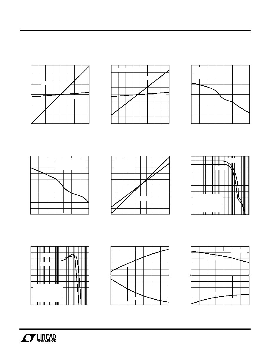
Input Bias Current vs
Current Source Mismatch
CURRENT SOURCE MISMATCH (%)
10
INPUT BIAS CURRENT (
µ
A)
5.0
0
5.0
10
LT1166 · TPC01
150
100
50
0
50
100
150
7.5
2.5
2.5
7.5
I
TOP
= I
BOTTOM
= 50mA
I
TOP
= I
BOTTOM
= 4mA
TEMPERATURE (
°
C)
50
OUTPUT OFFSET VOLTAGE (mV)
60
55
50
45
40
35
30
25
75
LT1166 · TPC03
25
0
50
100
125
R
L
=
I
TOP
= I
BOTTOM
= 15mA
R
IN
= 4.3k
Output Offset Voltage vs
Temperature
Output Offset Voltage vs
Current Source Mismatch
Input Bias Current vs
Temperature
TEMPERATURE (
°
C)
50
INPUT BIAS CURRENT (
µ
A)
3.0
2.9
2.8
2.7
2.6
2.5
2.4
2.3
2.2
2.1
2.0
0
50
75
LT1166 · TPC04
25
25
100
125
R
L
=
I
TOP
= I
BOTTOM
= 15mA
R
IN
= 4.3k
INPUT VOLTAGE (V)
10
OUTPUT VOLTAGE SWING (V)
10
8
6
4
2
0
2
4
6
8
10
6
LT1166 · TPC05
6
8
4
0
4
8
2
2
10
R
IN
= 4.3k
C
1
= C
2
= 500pF
R
L
= 10
SEE FIGURE 8
I
TOP
= I
BOTTOM
= 12mA
R
TOP
= R
BOTTOM
= 1k
Output Voltage vs Input Voltage
Open-Loop Voltage Gain vs
Frequency
Closed-Loop Voltage Gain vs
Frequency
Current Limit Pin Voltage vs
Temperature
FREQUENCY (MHz)
GAIN (dB)
2
1
0
1
2
3
4
5
6
7
8
0.001
0.1
1
10
LT1166 · TPC07
0.01
V
S
=
±
15V
R
IN
= 4.3k
I
TOP
= I
BOTTOM
= 12mA
C
1
= C
2
= 500pF
SEE FIGURE 8
R
L
=
R
L
=10
Voltage Across Sense Resistors
vs Temperature
TEMPERATURE (
°
C)
50
VOLTAGE DROP ACROSS SENSE RESISTORS (mV)
24
22
20
18
16
16
18
20
22
24
0
50
75
LT1166 · TPC08
25
25
100
125
SENSE
+
SENSE
TEMPERATURE (
°
C)
50
I
LIM
PIN VOLTAGE REFERENCED TO V
OUT
(V)
1.25
1.20
1.15
1.15
1.20
1.25
0
50
75
LT1166 · TPC09
25
25
100
125
PIN 7 TO PIN 3
PIN 6 TO PIN 3
V
IN
=
±
1.5V
I
TOP
AND I
BOTTOM
MISMATCH (mA)
1.0
OUTPUT OFFSET VOLTAGE (mV)
1.0
LT1166 · TPC02
0.5
0
0.5
800
600
400
200
0
200
400
600
800
0.75
0.25
0.25
0.75
I
TOP
= I
BOTTOM
= 50mA
R
IN
= 20k
R
IN
= 2k
FREQUENCY (MHz)
GAIN (dB)
30
25
20
15
10
5
0
5
10
15
20
0.001
0.1
1
10
LT1166 · TPC06
0.01
V
S
=
±
15V
R
IN
= 4.3k
I
TOP
= I
BOTTOM
= 12mA
C
1
= C
2
= 500pF
SEE FIGURE 8
R
L
=
R
L
=10
4
LT1166
TYPICAL PERFOR
M
A
N
CE CHARACTERISTICS
U
W
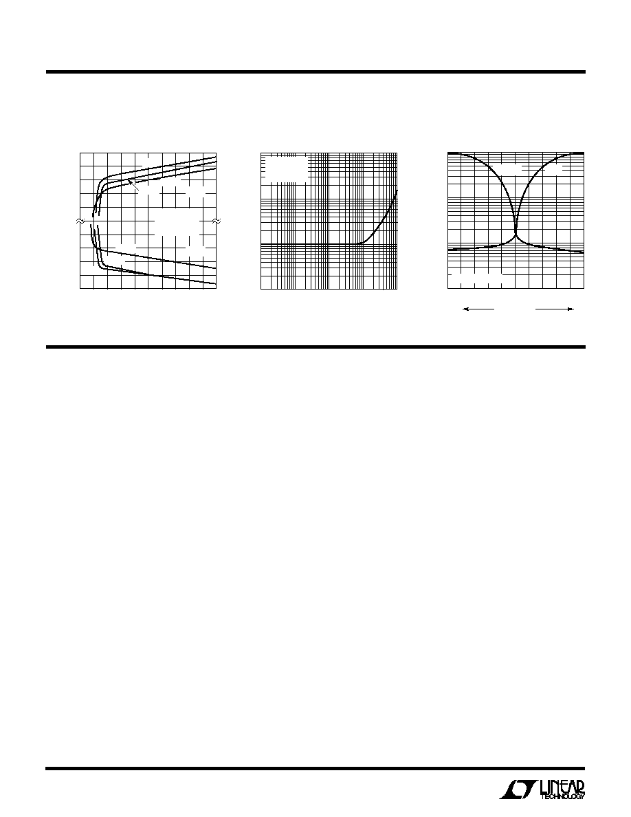
SUPPLY VOLTAGE (V)
0
INPUT TRANSCONDUCTANCE (mhos)
0.120
0.110
0.100
0.090
0.080
0.080
0.090
0.100
0.110
0.120
8
LT1166 · TPC10
2
1
3
5
7
9
4
6
10
V
IN
=
±
200mV
R
L
= 0
R
IN
= 0
125
°
C
25
°
C
55
°
C
125
°
C
55
°
C
25
°
C
gm
CC
gm
EE
Input Transconductance vs
Supply Voltage
LOAD CURRENT (mA)
10
8
6
4
2
0
2
4
6
8
10
SENSE PIN VOLTAGE REFERENCED TO V
OUT
(mV)
LT1166 · TPC12
1000
100
10
1
R
SENSE
= 100
V
BOTTOM
V
TOP
SINKING
SOURCING
Sense Pin Voltage Referenced to
V
OUT
vs Load Current
FREQUENCY (kHz)
0.1
TOTAL HARMONIC DISTORTION (%)
1
0.01
1
10
100
LT1166 · TPC11
0.01
0.1
10
R
L
= 10
P
O
= 1W
SEE FIGURE 8
Total Harmonic Distortion vs
Frequency
PI
N
FU
N
CTIO
N
S
U
U
U
V
TOP
(Pin 1): Pin 1 establishes the top side drive voltage
for the output transistors. Operating supply current enters
Pin 1 and a portion biases internal circuitry; Pin 1 current
should be greater than 4mA. Pin 1 voltage is internally
clamped to 12V with respect to V
OUT
and the pin current
should be limited to 75mA maximum.
V
IN
(Pin 2): Pin 2 is the input to a unity gain buffer which
drives V
OUT
(Pin 3). During a fault condition (short circuit)
the input impedance drops to 200
and the input current
must be limited to 5mA or V
IN
to V
OUT
limited to less than
±
6V.
V
OUT
(Pin 3): Pin 3 of the LT1166 is the output of a voltage
control loop that maintains the output voltage at the input
voltage.
V
BOTTOM
(Pin 4): Pin 4 establishes the bottom side drive
voltage for the output transistors. Operating supply cur-
rent exits this pin; Pin 4 current should be greater than
4mA. Pin 4 voltage is internally clamped to 12V with
respect to V
OUT
and the pin current should be limited to
75mA maximum.
SENSE
(Pin 5): The Sense
pin voltage is established
by the current control loop and it controls the output
quiescent current in the bottom side power device. Limit
the maximum differential voltage between Pin 5 and Pin 3
to
±
6V during fault conditions.
I
LIM
(Pin 6): The negative side current limit, limits the
voltage at V
BOTTOM
to V
OUT
during a negative fault condi-
tion. The maximum reverse voltage on Pin 6 with respect
to V
OUT
is 6V.
I
LIM
+
(Pin 7): The positive side current limit, limits the
voltage at V
TOP
to V
OUT
during a positive fault condition.
The maximum reverse voltage on Pin 7 with respect to
V
OUT
is 6V.
SENSE
+
(Pin 8): The Sense
+
pin voltage is established by
the current control loop and it controls the output quies-
cent current in the top side power device. Limit the
maximum differential voltage between Pin 8 and Pin 3 to
±
6V during fault conditions.
5
LT1166
APPLICATIO
N
S I
N
FOR
M
ATIO
N
W
U
U
U
Overvoltage Protection
The supplies V
TOP
(Pin 1) and V
BOTTOM
(Pin 4) have clamp
diodes that turn on when they exceed
±
12V. These diodes
act as ESD protection and serve to protect the LT1166
when used with large power MOS devices that produce
high V
GS
voltage. Current into Pin 1 or Pin 4 should be
limited to
±
75mA maximum.
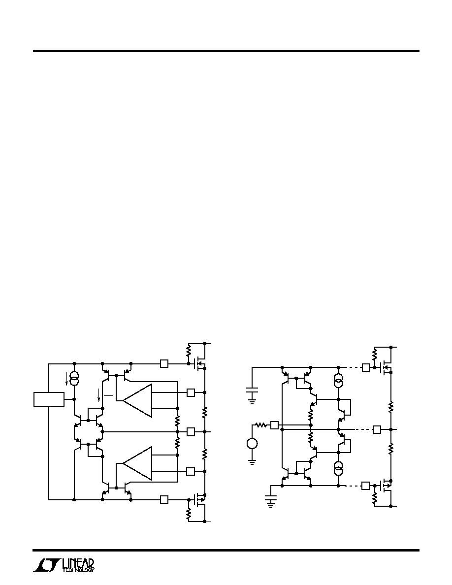
Multiplier Operation
Figure 2 shows the current multiplier circuit internal to the
LT1166 and how it works in conjunction with power
output transistors. The supply voltages V
T
(top) and V
B
(bottom) of the LT1166 are set by the required "on"
voltage of the power devices. A reference current I
REF
sets
a constant V
BE7
and V
BE8
. This voltage is across emitter
base of Q9 and Q10 which are 1/10 the emitter area of Q7
and Q8. The expression for this current multiplier is:
V
BE7
+ V
BE8
= V
BE9
+ V
BE10
or in terms of current:
(I
C9
)(I
C10
) = (I
REF
)
2
/100 = Constant
The product of I
C9
and I
C10
is constant. These currents are
mirrored and set the voltage on the (+) inputs of a pair of
internal op amps. The feedback of the op amps force the
same voltage on the () inputs and these voltages then
appear on the sense resistors in series with the power
devices. The product of the two currents in the power
devices is constant, as one increases the other decreases.
The excellent logging nature of Q9 and Q10 allows this
relation to hold over many decades in current.
The total current in Q7 and Q8 is actually the sum of I
REF
and a small error current from the shunt regulator. During
high output current conditions the error current from the
regulator decreases. Current conducted by the regulator
also decreases allowing V
T
or V
B
to increase by an amount
needed to drive the power devices.
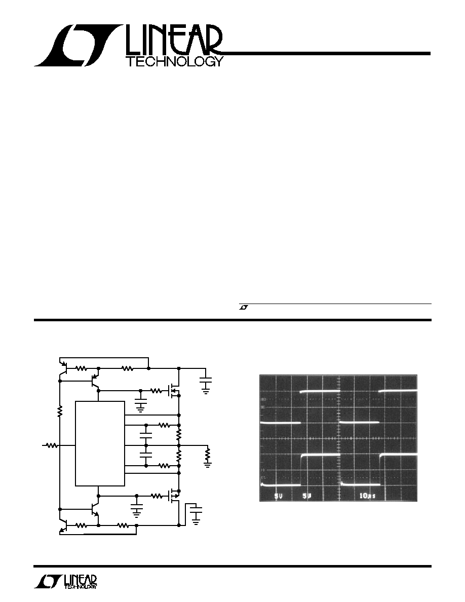
Driving the Input Stage
Figure 3 shows the input transconductance stage of the
LT1166 that provides a way to drive V
T
and V
B
. When a
positive voltage V
IN
is applied to R
IN
, a small input current
flows into R2 and the emitter of Q2. This effect causes V
O
to follow V
IN
within the gain error of the amplifier. The
input current is then mirrored by Q3/Q4 and current
supplied to Q4's collector is sourced by power device M1.
The signal current in Q4's emitter is absorbed by external
resistor R
B
and this causes V
B
to rise by the same amount
Figure 2. Constant Product Generator
V
AB
+
V
AB
1k
1k
1
1
8
1
3
5
4
V
O
V
V
+
Q7
×
10
Q8
×
10
Q9
×
1
Q10
×
1
R
B
1k
R
T
1k
+
+
M
2
V
TOP
V
BOTTOM
I
REF
I
REF
10
SHUNT
REGULATOR
1166 · F02
M
1
1
1
R1
R2
1
3
4
V
O
V
V
+
Q11
Q12
Q1
Q2
R
B
1k
R
T
1k
M
2
V
TOP
V
BOTTOM
1166 · F03
Q4
×
32
Q6
×
32
Q3
×
1
Q5
×
1
C
EXT1
V
IN
R
IN
C
EXT2
2
M
1
Figure 3. Input Stage Driving Gates