 | ÐлекÑÑоннÑй компоненÑ: LT1189 | СкаÑаÑÑ:  PDF PDF  ZIP ZIP |
Äîêóìåíòàöèÿ è îïèñàíèÿ www.docs.chipfind.ru
1
LT1189
Low Power
Video Difference Amplifier
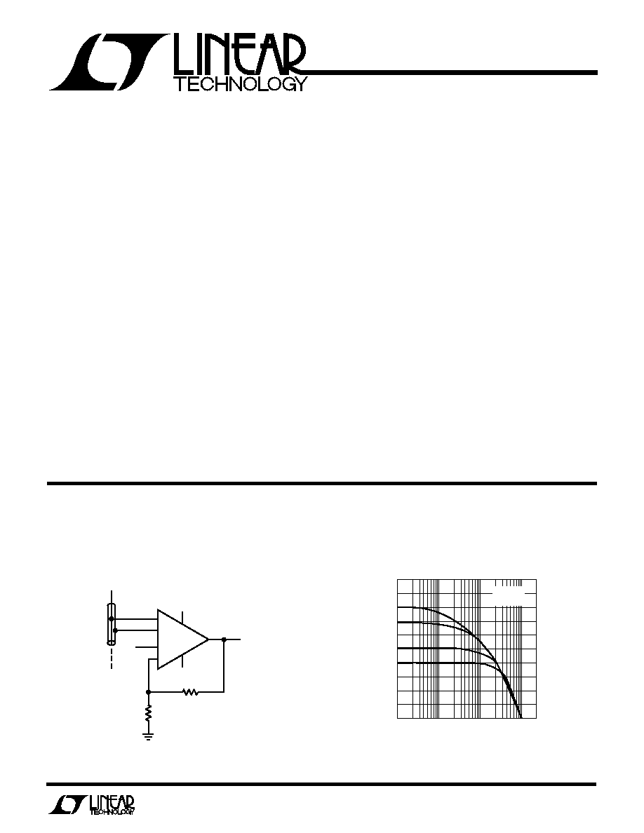
Closed-Loop Gain vs Frequency
Cable Sense Amplifier for Loop Through Connections
with DC Adjust
FREQUENCY (MHz)
0
VOLTAGE GAIN (dB)
10
20
30
40
0.1
10
100
LT1189 · TA02
1
V
S
= ±5V
R
L
= 1k
50
LT1189 · TA01
CABLE
V
DC
5V
7
6
LT1189
5V
4
+
+
3
1
2
8
909
V
OUT
V
IN
100
D
U
ESCRIPTIO
S
FEATURE
The LT1189 is a difference amplifier optimized for opera-
tion on
±
5V, or a single 5V supply, and gain
10. This
versatile amplifier features uncommitted high input im-
pedance (+) and () inputs, and can be used in differential
or single-ended configurations. Additionally, a second set
of inputs give gain adjustment and DC control to the
difference amplifier.
The LT1189's high slew rate, 220V/
µ
s, wide bandwidth,
35MHz, and
±
20mA output current require only 13mA of
supply current. The shutdown feature reduces the power
dissipation to a mere 15mW, and allows multiple amplifi-
ers to drive the same cable.
The LT1189 is a low power, gain of 10 stable version of the
popular LT1193, and is available in 8-pin miniDIPs and SO
packages. For lower gain applications see the LT1187
data sheet.
s
Differential or Single-Ended Gain Block (Adjustable)
s
3dB Bandwidth, A
V
=
±
10
35MHz
s
Slew Rate
220V/
µ
s
s
Low Supply Current
13mA
s
Output Current
±
20mA
s
CMRR at 10MHz
48dB
s
LT1193 Pin Out
s
Low Cost
s
Single 5V Operation
s
Drives Cables Directly
s
Output Shutdown
U
S
A
O
PPLICATI
s
Line Receivers
s
Video Signal Processing
s
Cable Drivers
s
Tape and Disc Drive Systems
U
A
O
PPLICATI
TYPICAL
LT1189
2
A
U
G
W
A
W
U
W
A
R
BSOLUTE
XI
TI
S
W
U
U
PACKAGE/ORDER I FOR ATIO
ORDER PART
NUMBER
Total Supply Voltage (V
+
to V
) ............................. 18V
Differential Input Voltage ........................................
±
6V
Input Voltage ..........................................................
±
V
S
Output Short Circuit Duration (Note 1) ........ Continuous
Operating Temperature Range
LT1189M ..................................... 55
°
C to 150
°
C
LT1189C............................................. 0
°
C to 70
°
C
Junction Temperature (Note 2)
Plastic Package (CN8,CS8) ......................... 150
°
C
Ceramic Package (CJ8,MJ8) ....................... 175
°
C
Storage Temperature Range ................ 65
°
C to 150
°
C
Lead Temperature (Soldering, 10 sec.)................ 300
°
C
S8 PART MARKING
LT1189MJ8
LT1189CJ8
LT1189CN8
LT1189CS8
LT1189M/C
SYMBOL
PARAMETER
CONDITIONS
MIN
TYP
MAX
UNITS
V
OS
Input Offset Voltage
Either Input, (Note 4)
1.0
3.0
mV
SOIC Package
1.0
4.0
mV
I
OS
Input Offset Current
Either Input
0.2
1.0
µ
A
I
B
Input Bias Current
Either Input
±
0.5
±
2.0
µ
A
e
n
Input Noise Voltage
f
O
= 10kHz
30
nV/
Hz
i
n
Input Noise Current
f
O
= 10kHz
1.25
pA/
Hz
R
IN
Input Resistance
Differential
30
k
C
IN
Input Capacitance
Either Input
2.0
pF
V
IN
LIM
Input Voltage Limit
(Note 5)
±
170
mV
Input Voltage Range
2.5
3.5
V
CMRR
Common-Mode Rejection Ratio
V
CM
= 2.5V to 3.5V
80
105
dB
PSRR
Power Supply Rejection Ratio
V
S
=
±
2.375V to
±
8V
75
90
dB
V
OUT
Output Voltage Swing
V
S
=
±
5V, R
L
= 1k, A
V
= 50
±
3.8
±
4.0
V
V
S
=
±
8V, R
L
= 1k, A
V
= 50
±
6.7
±
7.0
V
S
=
±
8V, R
L
= 300
, A
V
= 50, (Note 3)
±
6.4
±
6.8
G
E
Gain Error
V
O
=
±
1.0V, A
V
= 10
1.0
3.5
%
SR
Slew Rate
(Note 6, 10)
150
220
V/
µ
s
FPBW
Full Power Bandwidth
V
O
= 2V
P-P
, (Note 7)
35
MHz
BW
Small Signal Bandwidth
A
V
= 10
35
MHz
t
r
, t
f
Rise Time, Fall Time
A
V
= 50, V
O
=
±
1.5V, 20% to 80% (Note 10)
35
50
75
ns
t
PD
Propagation Delay
R
L
= 1k, V
O
=
±
125mV, 50% to 50%
12
ns
Overshoot
V
O
=
±
50mV
10
%
t
s
Settling Time
3V Step, 0.1%, (Note 8)
1
µ
s
Diff A
V
Differential Gain
R
L
= 1k, A
V
= 10, (Note 9)
0.6
%
Diff Ph
Differential Phase
R
L
= 1k, A
V
= 10, (Note 9)
0.75
DEG
P-P
I
S
Supply Current
13
16
mA
Shutdown Supply Current
Pin 5 at V
0.8
1.5
mA
V
S
=
±
5V, V
REF
= 0V, R
FB1
= 900
from pins 6 to 8, R
FB2
= 100
from pin 8 to ground, R
L
= R
FB1
+ R
FB2
= 1k, C
L
10pF, pin 5 open.
ELECTRICAL C
C
HARA TERISTICS
T
A
= 25
°
C, (Note 3)
5V
+
8
7
6
5
4
3
2
1
+/REF
IN
+IN
V
S/D
OUT
+
V
/FB
TOP VIEW
S8 PACKAGE
8-LEAD PLASTIC SOIC
N8 PACKAGE
8-LEAD PLASTIC DIP
J8 PACKAGE
8-LEAD HERMETIC DIP
LT1189 · POI01
1189
T
JMAX
= 175
°
C,
JA
= 100
°
C/ W (J8)
T
JMAX
= 150
°
C,
JA
= 100
°
C/ W (N8)
T
JMAX
= 150
°
C,
JA
= 150
°
C/ W (S8)
3
LT1189
V
S
=
±
5V, V
REF
= 0V, R
FB1
= 900
from pins 6 to 8, R
FB2
= 100
from pin 8 to ground, R
L
= R
FB1
+ R
FB2
= 1k, C
L
10pF, pin 5 open.
LT1189M
SYMBOL
PARAMETER
CONDITIONS
MIN
TYP
MAX
UNITS
V
OS
Input Offset Voltage
Either Input, (Note 4)
1.0
7.5
mV
V
OS
/
T
Input V
OS
Drift
10
µ
V/
°
C
I
OS
Input Offset Current
Either Input
0.2
1.5
µ
A
I
B
Input Bias Current
Either Input
±
0.5
±
3.5
µ
A
Input Voltage Range
2.5
3.5
V
CMRR
Common-Mode Rejection Ratio
V
CM
= 2.5V to 3.5V
80
105
dB
PSRR
Power Supply Rejection Ratio
V
S
=
±
2.375V to
±
8V
65
90
dB
V
OUT
Output Voltage Swing
V
S
=
±
5V, R
L
= 1k, A
V
= 50
±
3.7
±
4.0
V
V
S
=
±
8V, R
L
= 1k, A
V
= 50
±
6.6
±
7.0
V
S
=
±
8V, R
L
= 300
, A
V
= 50, (Note 3)
±
6.4
±
6.6
G
E
Gain Error
V
O
=
±
1V, A
V
= 10, R
L
= 1k
1.0
6.0
%
I
S
Supply Current
13
17
mA
Shutdown Supply Current
Pin 5 at V
, (Note 11)
0.8
1.5
mA
I
S/D
Shutdown Pin Current
Pin 5 at V
5
25
µ
A
V
S
=
±
5V, V
REF
= 0V, R
FB1
= 900
from pins 6 to 8, R
FB2
= 100
from pin 8 to ground, R
L
= R
FB1
+ R
FB2
= 1k, C
L
10pF, pin 5 open.
ELECTRICAL C
C
HARA TERISTICS
T
A
= 25
°
C, (Note 3)
5V
+
LT1189M/C
SYMBOL
PARAMETER
CONDITIONS
MIN
TYP
MAX
UNITS
I
S/D
Shutdown Pin Current
Pin 5 at V
5
25
µ
A
t
on
Turn On Time
Pin 5 from V
to Ground, R
L
= 1k
500
ns
t
off
Turn Off Time
Pin 5 from Ground to V
, R
L
= 1k
600
ns
LT1189M/C
SYMBOL
PARAMETER
CONDITIONS
MIN
TYP
MAX
UNITS
V
OS
Input Offset Voltage
Either Input, (Note 4)
1.0
3.0
mV
SOIC Package
1.0
5.0
mV
I
OS
Input Offset Current
Either Input
0.2
1.0
µ
A
I
B
Input Bias Current
Either Input
±
0.5
±
2.0
µ
A
Input Voltage Range
2.0
3.5
V
CMRR
Common-Mode Rejection Ratio
V
CM
= 2.0V to 3.5V
80
100
dB
V
OUT
Output Voltage Swing
R
L
= 300
to Ground
V
OUT
High
3.6
4.0
V
(Note 3)
V
OUT
Low
0.15
0.4
SR
Slew Rate
V
O
= 1.5V to 3.5V
175
V/
µ
s
BW
Small-Signal Bandwidth
A
V
= 10
30
MHz
I
S
Supply Current
12
15
mA
Shutdown Supply Current
Pin 5 at V
0.8
1.5
mA
I
S/D
Shutdown Pin Current
Pin 5 at V
5
25
µ
A
V
S
+
= 5V, V
S
= 0V, V
REF
= 2.5V, R
FB1
= 900
from pins 6 to 8, R
FB2
= 100
from pin 8 to V
REF
, R
L
= R
FB1
+ R
FB2
= 1k, C
L
10pF, pin 5
open.
5V
+
ELECTRICAL C
C
HARA TERISTICS
55
°
C
T
A
125
°
C, (Note 3)
T
A
= 25
°
C, (Note 3)
5V ELECTRICAL C
C
HARA TERISTICS
LT1189
4
LT1189C
SYMBOL
PARAMETER
CONDITIONS
MIN
TYP
MAX
UNITS
V
OS
Input Offset Voltage
Either Input
1.0
3.0
mV
(Note 4)
SOIC Package
1.0
6.0
mV
V
OS
/
T
Input V
OS
Drift
5.0
µ
V/
°
C
I
OS
Input Offset Current
Either Input
0.2
1.5
µ
A
I
B
Input Bias Current
Either Input
±
0.5
±
3.5
µ
A
Input Voltage Range
2.5
3.5
V
CMRR
Common-Mode Rejection Ratio
V
CM
= 2.5V to 3.5V
80
105
dB
PSRR
Power Supply Rejection Ratio
V
S
=
±
2.375V to
±
8V
70
90
dB
V
OUT
Output Voltage Swing
V
S
=
±
5V, R
L
= 1k, A
V
= 50
±
3.7
±
4.0
V
V
S
=
±
8V, R
L
= 1k, A
V
= 50
±
6.6
±
7.0
V
S
=
±
8V, R
L
= 300
, A
V
= 50, (Note 3)
±
6.4
±
6.6
G
E
Gain Error
V
O
=
±
1V, A
V
= 10, R
L
= 1k
1.0
3.5
%
I
S
Supply Current
13
17
mA
Shutdown Supply Current
Pin 5 at V
, (Note 11)
0.8
1.5
mA
I
S/D
Shutdown Pin Current
Pin 5 at V
5
25
µ
A
V
S
=
±
5V, V
REF
= 0V, R
FB1
= 900
from pins 6 to 8, R
FB2
= 100
from pin 8 to ground, R
L
= R
FB1
+ R
FB2
= 1k, C
L
10pF, pin 5 open.
Note 1: A heat sink may be required to keep the junction temperature below
absolute maximum when the output is shorted continuously.
Note 2: T
J
is calculated from the ambient temperature T
A
and power dissipation
P
D
according to the following formulas:
LT1189MJ8, LT1189CJ8:
T
J
= T
A
+ (P
D
×
100
°
C/W)
LT1189CN8:
T
J
= T
A
+ (P
D
×
100
°
C/W)
LT1189CS8:
T
J
= T
A
+ (P
D
×
150
°
C/W)
Note 3: When R
L
= 1k is specified, the load resistor is R
FB1
+ R
FB2
, but when
R
L
= 300
is specified, then an additional 430
is added to the output such
that (R
FB1
+ R
FB2
) in parallel with 430
is R
L
= 300
.
Note 4: V
OS
measured at the output (pin 6) is the contribution from both input
pair, and is input referred.
Note 5: V
IN
LIM
is the maximum voltage between V
IN
and +V
IN
(pin 2 and
pin 3) for which the output can respond.
Note 6: Slew rate is measured between
±
1V on the output, with a V
IN
step of
±
0.5V, A
V
= 10 and R
L
= 1k.
Note 7: Full power bandwidth is calculated from the slew rate measurement:
FPBW = SR/2
Vp.
Note 8: Settling time measurement techniques are shown in "Take the
Guesswork Out of Settling Time Measurements," EDN, September 19, 1985.
Note 9: NTSC (3.58MHz).
Note 10: AC parameters are 100% tested on the ceramic and plastic DIP
packaged parts (J8 and N8 suffix) and are sample tested on every lot of the SO
packaged parts (S8 suffix).
Note 11: See Application section for shutdown at elevated temperatures. Do
not operate shutdown above T
J
> 125
°
C.
5V
+
ELECTRICAL C
C
HARA TERISTICS
0
°
C
T
A
70
°
C, (Note 3)
LT1189C
SYMBOL
PARAMETER
CONDITIONS
MIN
TYP
MAX
UNITS
V
OS
Input Offset Voltage, (Note 4)
Either Input
1.0
3.0
mV
V
OS
/
T
Input V
OS
Drift
5.0
µ
V/
°
C
I
OS
Input Offset Current
Either Input
0.2
1.5
µ
A
I
B
Input Bias Current
Either Input
±
0.5
±
3.5
µ
A
Input Voltage Range
2.0
3.5
V
CMRR
Common-Mode Rejection Ratio
V
CM
= 2.0V to 3.5V
80
100
dB
V
OUT
Output Voltage Swing
R
L
= 300
to Ground
V
OUT
High
3.5
4.0
V
(Note 3)
V
OUT
Low
0.15
0.4
I
S
Supply Current
12
16
mA
Shutdown Supply Current
Pin 5 at V, (Note 11)
0.8
1.5
mA
I
S/D
Shutdown Pin Current
Pin 5 at V
5
25
µ
A
5V
V
S
+
= +5V, V
S
= 0V, V
REF
= 2.5V, R
FB1
= 900
from pins 6 to 8, R
FB2
= 100
from pin 8 to V
REF
, R
L
= R
FB1
+ R
FB2
= 1k, C
L
10pF, pin 5
open.
0
°
C
T
A
70
°
C, (Note 3)
ELECTRICAL C
C
HARA TERISTICS
5
LT1189
C
C
HARA TERISTICS
U
W
A
TYPICAL PERFOR
CE
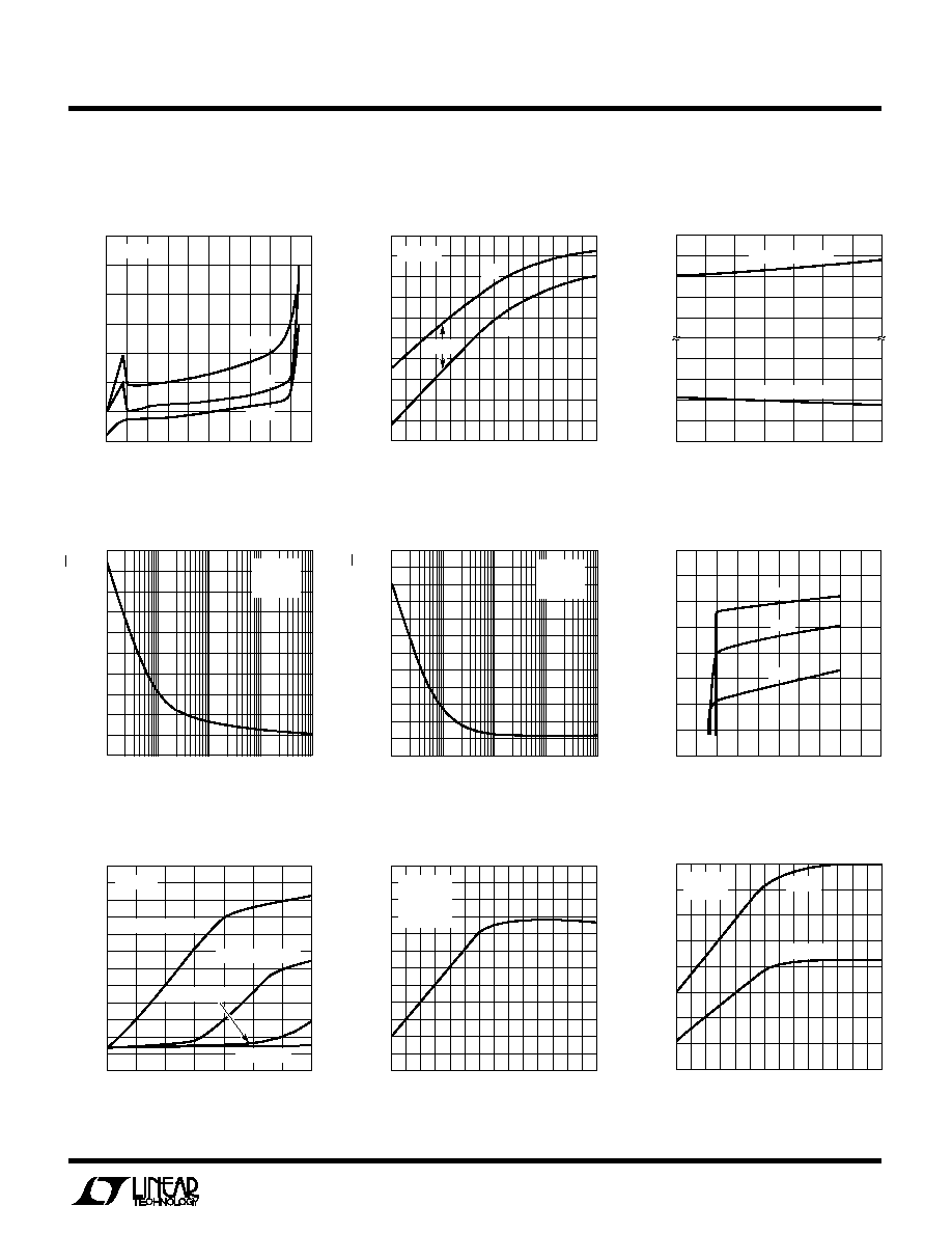
Input Bias Current vs
Common-Mode Voltage vs
Common-Mode Voltage
Input Bias Current vs Temperature
Temperature
COMMON-MODE VOLTAGE (V)
5
0.5
INPUT BIAS CURRENT ( A)
0
0.5
1.5
2.5
3
0
2
4
LT1189 · TPC01
µ
4
2
1
3
125°C
55°C
25°C
V
S
= ±5V
1
5
1.0
2.0
3.0
TEMPERATURE (°C)
50
400
INPUT BIAS CURRENT (nA)
300
200
100
0
100
0
25
75
125
LT1189 · TPC02
25
50
100
+I
B
I
B
I
OS
V
S
= ±5V
Equivalent Input Noise Voltage vs
Equivalent Input Noise Current vs
Frequency
Frequency
Supply Current vs Supply Voltage
FREQUENCY (Hz)
EQUIVALENT INPUT NOISE VOLTAGE (nV/ Hz)
120
160
10
1k
10k
100k
LT1189 · TPC04
0
100
80
V = ±5V
T = 25°C
R = 0
S
A
S
40
200
60
140
100
180
20
FREQUENCY (Hz)
2
EQUIVALENT INPUT NOISE CURRENT (pA/ Hz)
12
10
1k
10k
100k
LT1189 · TPC05
0
100
6
4
8
10
V
S
= ±5V
T
A
= 25°C
R
S
= 100k
±SUPPLY VOLTAGE (V)
0
8
SUPPLY CURRENT (mA)
12
14
16
2
4
6
10
LT1189 · TPC06
8
55°C
25°C
125°C
10
Shutdown Supply Current vs
Temperature
Gain Error vs Temperature
Open-Loop Gain vs Temperature
TEMPERATURE (°C)
50
0
SHUTDOWN SUPPLY CURRENT (mA)
2.0
3.0
4.0
5.0
6.0
0
25
75
125
LT1189 · TPC07
1.0
25
50
100
V = ±5V
S
V
S/D
= V
EE
+ 0.6V
V
S/D
= V
EE
+ 0.4V
V
S/D
= V
EE
V
S/D
= V
EE
+ 0.2V
TEMPERATURE (°C)
GAIN ERROR (%)
LT1189 · TPC08
50
2.4
1.6
1.2
0
50
100
125
2.0
25
25
75
1.4
1.8
2.2
V
S
= ±5V
V
OUT
= ±1V
A
V
= 10
R
L
= 1k
0
OPEN-LOOP GAIN (kV/
V)
4
8
12
16
TEMPERATURE (°C)
50
0
50
100
125
LT1189 · TPC09
25
25
75
R
L
= 1k
R
L
= 500
V
S
= ±5V
V
O
= ±3V
14
10
6
2
TEMPERATURE (°C)
COMMON-MODE RANGE (V)
2.0
V
+
50
25
75
125
LT1189 · TPC03
V
0
1.0
1.0
2.0
0.5
1.5
1.5
0.5
25
50
100
V
+
= 1.8V TO 9V
V
+
= 1.8V TO 9V