 | –≠–ª–µ–∫—Ç—Ä–æ–Ω–Ω—ã–π –∫–æ–º–ø–æ–Ω–µ–Ω—Ç: LT1210 | –°–∫–∞—á–∞—Ç—å:  PDF PDF  ZIP ZIP |
1
LT1210
1.1A, 35MHz Current
Feedback Amplifier
D
U
ESCRIPTIO
S
FEATURE
s
1.1A Minimum Output Drive Current
s
35MHz Bandwidth, A
V
= 2, R
L
= 10
s
900V/
µ
s Slew Rate, A
V
= 2, R
L
= 10
s
High Input Impedance: 10M
s
Wide Supply Range:
±
5V to
±
15V
(TO-220 and DD Packages)
s
Enhanced
JA
SO-16 Package for
±
5V Operation
s
Shutdown Mode: I
S
< 200
µ
A
s
Adjustable Supply Current
s
Stable with C
L
= 10,000pF
The LT
Æ
1210 is a current feedback amplifier with high
output current and excellent large-signal characteristics.
The combination of high slew rate, 1.1A output drive and
±
15V operation enables the device to deliver significant
power at frequencies in the 1MHz to 2MHz range. Short-
circuit protection and thermal shutdown ensure the
device's ruggedness. The LT1210 is stable with large
capacitive loads, and can easily supply the large currents
required by the capacitive loading. A shutdown feature
switches the device into a high impedance and low
supply current mode, reducing dissipation when the
device is not in use. For lower bandwidth applications,
the supply current can be reduced with a single external
resistor.
The LT1210 is available in the TO-220 and DD packages
for operation with supplies up to
±
15V. For
±
5V applica-
tions the device is also available in a low thermal resis-
tance SO-16 package.
s
Cable Drivers
s
Buffers
s
Test Equipment Amplifiers
s
Video Amplifiers
s
ADSL Drivers
APPLICATIO
N
S
U
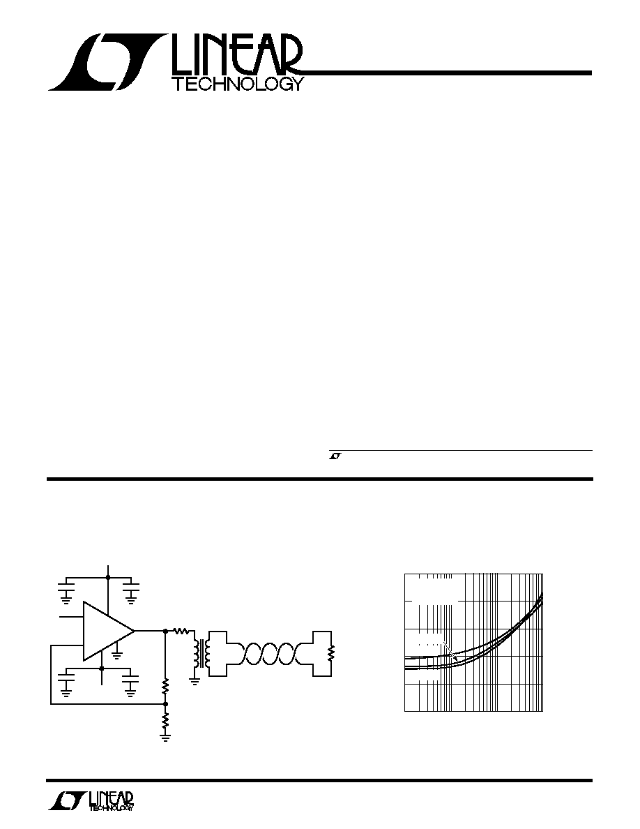
TYPICAL APPLICATIO S
U
≠
+
+
LT1210
V
IN
+
4.7
µ
F*
4.7
µ
F*
100nF
1210 TA01
R
T
11
2.5W
T1**
845
3
1
274
100nF
SD
15V
≠15V
* TANTALUM
** MIDCOM 671-7783 OR EQUIVALENT
R
L
100
2.5W
Total Harmonic Distortion vs Frequency
FREQUENCY (Hz)
1k
TOTAL HARMONIC DISTORTION (dB)
≠50
≠60
≠70
≠80
≠90
≠100
10k
100k
1M
1210 TA02
V
S
=
±
15V
V
OUT
= 20V
P-P
A
V
= 4
R
L
= 10
R
L
= 50
R
L
= 12.5
Twisted Pair Driver
, LTC and LT are registered trademarks of Linear Technology Corporation.
2
LT1210
A
U
G
W
A
W
U
W
A
R
BSOLUTE
XI
TI
S
Supply Voltage .....................................................
±
18V
Input Current ....................................................
±
15mA
Output Short-Circuit Duration (Note 1) ....... Continuous
Specified Temperature Range (Note 2) ...... 0
∞
C to 70
∞
C
Operating Temperature Range ............... ≠40
∞
C to 85
∞
C
Junction Temperature ......................................... 150
∞
C
Storage Temperature Range ................. ≠ 65
∞
C to 150
∞
C
Lead Temperature (Soldering, 10 sec) ................. 300
∞
C
SYMBOL
PARAMETER
CONDITIONS
MIN
TYP
MAX
UNITS
V
OS
Input Offset Voltage
T
A
= 25
∞
C
±
3
±
15
mV
q
±
20
mV
Input Offset Voltage Drift
q
10
µ
V/
∞
C
I
IN
+
Noninverting Input Current
T
A
= 25
∞
C
±
2
±
5
µ
A
q
±
20
µ
A
I
IN
≠
Inverting Input Current
T
A
= 25
∞
C
±
10
±
60
µ
A
q
±
100
µ
A
e
n
Input Noise Voltage Density
f = 10kHz, R
F
= 1k, R
G
= 10
, R
S
= 0
3.0
nV/
Hz
+ i
n
Input Noise Current Density
f = 10kHz, R
F
= 1k, R
G
= 10
, R
S
= 10k
2.0
pA/
Hz
≠ i
n
Input Noise Current Density
f = 10kHz, R
F
= 1k, R
G
= 10
, R
S
= 10k
40
pA/
Hz
R
IN
Input Resistance
V
IN
=
±
12V, V
S
=
±
15V
q
1.50
10
M
V
IN
=
±
2V, V
S
=
±
5V
q
0.25
5
M
C
IN
Input Capacitance
V
S
=
±
15V
2
pF
Input Voltage Range
V
S
=
±
15V
q
±
12
±
13.5
V
V
S
=
±
5V
q
±
2
±
3.5
V
V
CM
= 0V,
±
5V
V
S
±
15V, pulse tested, V
SD
= 0V, unless otherwise noted.
ELECTRICAL CHARACTERISTICS
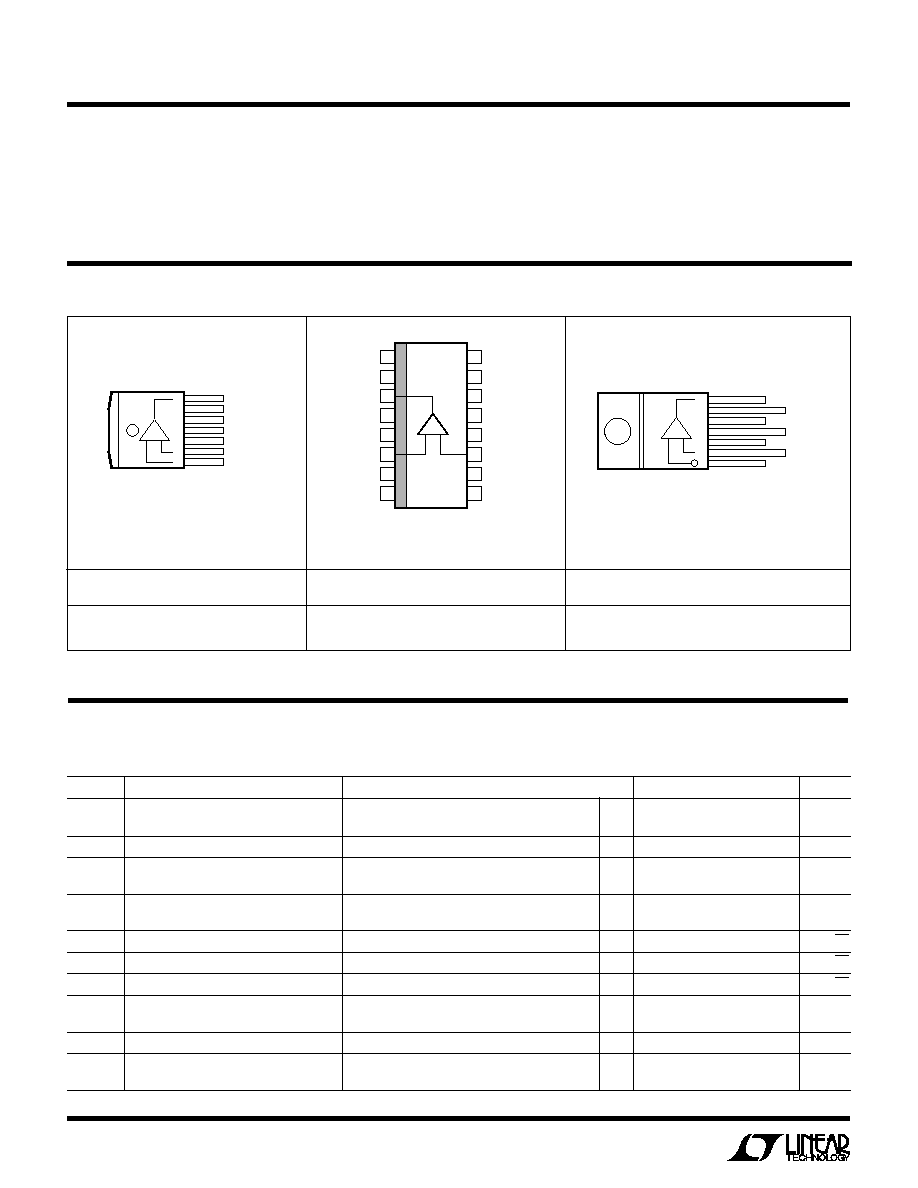
TOP VIEW
S PACKAGE
16-LEAD PLASTIC SO
1
2
3
4
5
6
7
8
16
15
14
13
12
11
10
9
V
+
V
+
OUT
V
+
NC
≠IN
NC
V
+
V
+
NC
V
≠
COMP
SHUTDOWN
+IN
NC
V
+
JA
40
∞
C/W (Note 3)
JA
25
∞
C/W
R PACKAGE
7-LEAD PLASTIC DD
FRONT VIEW
OUT
V
≠
COMP
V
+
SHUTDOWN
+IN
≠IN
7
6
5
4
3
2
1
TAB
IS V
+
T7 PACKAGE
7-LEAD TO-220
OUT
V
≠
COMP
V
+
SHUTDOWN
+IN
≠IN
FRONT VIEW
7
6
5
4
3
2
1
TAB
IS V
+
JC
= 5
∞
C/W
ORDER PART NUMBER
LT1210CR
LT1210CT7
ORDER PART NUMBER
ORDER PART NUMBER
LT1210CS
Consult factory for Industrial and Military grade parts.
PACKAGE/ORDER I
N
FOR
M
ATIO
N
W
U
U

3
LT1210
SYMBOL
PARAMETER
CONDITIONS
MIN
TYP
MAX
UNITS
CMRR
Common Mode Rejection Ratio
V
S
=
±
15V, V
CM
=
±
12V
q
55
62
dB
V
S
=
±
5V, V
CM
=
±
2V
q
50
60
dB
Inverting Input Current
V
S
=
±
15V, V
CM
=
±
12V
q
0.1
10
µ
A/V
Common Mode Rejection
V
S
=
±
5V, V
CM
=
±
2V
q
0.1
10
µ
A/V
PSRR
Power Supply Rejection Ratio
V
S
=
±
5V to
±
15V
q
60
77
dB
Noninverting Input Current
V
S
=
±
5V to
±
15V
q
30
500
nA/V
Power Supply Rejection
Inverting Input Current
V
S
=
±
5V to
±
15V
q
0.7
5
µ
A/V
Power Supply Rejection
A
V
Large-Signal Voltage Gain
T
A
= 25
∞
C, V
S
=
±
15V, V
OUT
=
±
10V,
55
71
dB
R
L
= 10
(Note 3)
V
S
=
±
15V, V
OUT
=
±
8.5V, R
L
= 10
(Note 3)
q
55
68
dB
V
S
=
±
5V, V
OUT
=
±
2V, R
L
= 10
q
55
68
dB
R
OL
Transresistance,
V
OUT
/
I
IN
≠
T
A
= 25
∞
C, V
S
=
±
15V, V
OUT
=
±
10V,
R
L
= 10
(Note 3)
100
260
k
V
S
=
±
15V, V
OUT
=
±
8.5V, R
L
= 10
(Note 3)
q
75
200
k
V
S
=
±
5V, V
OUT
=
±
2V, R
L
= 10
q
75
200
k
V
OUT
Maximum Output Voltage Swing
T
A
= 25
∞
C, V
S
=
±
15V, R
L
= 10
(Note 3)
±
10.0
±
11.5
V
q
±
8.5
V
T
A
= 25
∞
C, V
S
=
±
5V, R
L
= 10
±
2.5
±
3.0
V
q
±
2.0
V
I
OUT
Maximum Output Current (Note 3)
V
S
=
±
15V, R
L
= 1
q
1.1
2.0
A
I
S
Supply Current (Note 3)
T
A
= 25
∞
C, V
S
=
±
15V, V
SD
= 0V
35
50
mA
q
65
mA
Supply Current, R
SD
= 51k (Notes 3, 4)
T
A
= 25
∞
C, V
S
=
±
15V
15
30
mA
Positive Supply Current, Shutdown
V
S
=
±
15V, V
SD
= 15V
q
200
µ
A
Output Leakage Current, Shutdown
V
S
=
±
15V, V
SD
= 15V
q
10
µ
A
SR
Slew Rate (Note 5)
T
A
= 25
∞
C, A
V
= 2, R
L
= 400
400
900
V/
µ
s
Slew Rate (Note 3)
T
A
= 25
∞
C, A
V
= 2, R
L
= 10
900
V/
µ
s
Differential Gain (Notes 3, 6)
V
S
=
±
15V, R
F
= 750
, R
G
= 750
, R
L
= 15
0.3
%
Differential Phase (Notes 3, 6)
V
S
=
±
15V, R
F
= 750
, R
G
= 750
, R
L
= 15
0.1
DEG
BW
Small-Signal Bandwidth
A
V
= 2, V
S
=
±
15V, Peaking
1dB,
55
MHz
R
F
= R
G
= 680
, R
L
= 100
A
V
= 2, V
S
=
±
15V, Peaking
1dB,
35
MHz
R
F
= R
G
= 576
, R
L
= 10
ELECTRICAL CHARACTERISTICS
V
CM
= 0V,
±
5V
V
S
±
15V, pulse tested, V
SD
= 0V, unless otherwise noted.
supply voltages greater than
±
5V, use the TO-220 or DD package. See
"Thermal Considerations" in the Applications Information section for
details on calculating junction temperature. If the maximum dissipation of
the package is exceeded, the device will go into thermal shutdown.
Note 4: R
SD
is connected between the Shutdown pin and ground.
Note 5: Slew rate is measured at
±
5V on a
±
10V output signal while
operating on
±
15V supplies with R
F
= 1.5k, R
G
= 1.5k and R
L
= 400
.
Note 6: NTSC composite video with an output level of 2V.
The
q
denotes specifications which apply for 0
∞
C
T
A
70
∞
C.
Note 1: Applies to short circuits to ground only. A short circuit between
the output and either supply may permanently damage the part when
operated on supplies greater than
±
10V.
Note 2: Commercial grade parts are designed to operate over the
temperature range of ≠ 40
∞
C
T
A
85
∞
C, but are neither tested nor
guaranteed beyond 0
∞
C
T
A
70
∞
C. Industrial grade parts tested over
≠ 40
∞
C
T
A
85
∞
C are available on special request. Consult factory.
Note 3: SO package is recommended for
±
5V supplies only, as the power
dissipation of the SO package limits performance on higher supplies. For
4
LT1210
R
SD
= 0
, I
S
= 30mA, V
S
=
±
5V, Peaking
1dB
≠ 3dB BW
A
V
R
L
R
F
R
G
(MHz)
≠ 1
150
549
549
52.5
30
590
590
39.7
10
619
619
26.5
1
150
604
≠
53.5
30
649
≠
39.7
10
619
≠
27.4
2
150
562
562
51.8
30
590
590
38.8
10
576
576
27.4
10
150
392
43.2
48.4
30
383
42.2
40.3
10
215
23.7
36.0
R
SD
= 0
, I
S
= 35mA, V
S
=
±
15V, Peaking
1dB
≠ 3dB BW
A
V
R
L
R
F
R
G
(MHz)
≠ 1
150
604
604
66.2
30
649
649
48.4
10
665
665
46.5
1
150
750
≠
56.8
30
866
≠
35.4
10
845
≠
24.7
2
150
665
665
52.5
30
715
715
38.9
10
576
576
35.0
10
150
453
49.9
61.5
30
432
47.5
43.1
10
221
24.3
45.5
R
SD
= 7.5k, I
S
= 15mA, V
S
=
±
5V, Peaking
1dB
≠ 3dB BW
A
V
R
L
R
F
R
G
(MHz)
≠ 1
150
562
562
39.7
30
619
619
28.9
10
604
604
20.5
1
150
634
≠
41.9
30
681
≠
29.7
10
649
≠
20.7
2
150
576
576
40.2
30
604
604
29.6
10
576
576
21.6
10
150
324
35.7
39.5
30
324
35.7
32.3
10
210
23.2
27.7
R
SD
= 47.5k, I
S
= 18mA, V
S
=
±
15V, Peaking
1dB
≠ 3dB BW
A
V
R
L
R
F
R
G
(MHz)
≠ 1
150
619
619
47.8
30
698
698
32.3
10
698
698
22.2
1
150
732
≠
51.4
30
806
≠
33.9
10
768
≠
22.5
2
150
634
634
48.4
30
698
698
33.0
10
681
681
22.5
10
150
348
38.3
46.8
30
357
39.2
36.7
10
205
22.6
31.3
R
SD
= 15k, I
S
= 7.5mA, V
S
=
±
5V, Peaking
1dB
≠ 3dB BW
A
V
R
L
R
F
R
G
(MHz)
≠ 1
150
536
536
28.2
30
549
549
20.0
10
464
464
15.0
1
150
619
≠
28.6
30
634
≠
19.8
10
511
≠
14.9
2
150
536
536
28.3
30
549
549
19.9
10
412
412
15.7
10
150
150
16.5
31.5
30
118
13.0
27.1
10
100
11.0
19.4
R
SD
= 82.5k, I
S
= 9mA, V
S
=
±
15V, Peaking
1dB
≠ 3dB BW
A
V
R
L
R
F
R
G
(MHz)
≠ 1
150
590
590
34.8
30
649
649
22.5
10
576
576
16.3
1
150
715
≠
35.5
30
768
≠
22.5
10
649
≠
16.1
2
150
590
590
35.3
30
665
665
22.5
10
549
549
16.8
10
150
182
20.0
37.2
30
182
20.0
28.9
10
100
11.0
22.5
S
M
ALL-SIG
N
AL BA
N
DWIDTH
U
U
W
5
LT1210
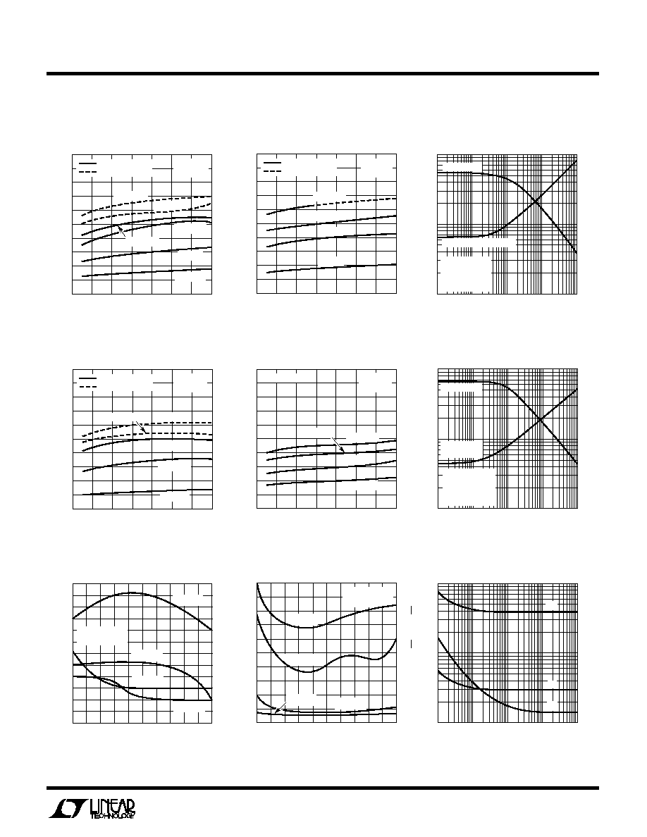
TYPICAL PERFOR A CE CHARACTERISTICS
W U
Bandwidth vs Supply Voltage
4
0
20
50
8
12
10
40
30
6
10
14
16
18
SUPPLY VOLTAGE (
±
V)
≠
3dB BANDWIDTH (MHz)
1210 G02
PEAKING
1dB
PEAKING
5dB
R
F
= 560
R
F
= 1k
R
F
= 2k
R
F
= 750
A
V
= 2
R
L
= 10
4
0
10
30
40
50
100
70
8
12
20
80
90
60
6
10
14
16
18
SUPPLY VOLTAGE (
±
V)
≠
3dB BANDWIDTH (MHz)
1210 G01
PEAKING
1dB
PEAKING
5dB
R
F
= 470
R
F
= 560
R
F
= 750
R
F
= 1k
R
F
= 1.5k
A
V
= 2
R
L
= 100
R
F
= 680
4
0
10
30
40
50
100
70
8
12
20
80
90
60
6
10
14
16
18
SUPPLY VOLTAGE (
±
V)
≠
3dB BANDWIDTH (MHz)
1210 G04
PEAKING
1dB
PEAKING
5dB
R
F
= 470
R
F
= 1.5k
R
F
= 330
R
F
= 680
R
F
=390
A
V
= 10
R
L
= 100
Bandwidth vs Supply Voltage
4
0
20
50
8
12
10
40
30
6
10
14
16
18
SUPPLY VOLTAGE (
±
V)
≠
3dB BANDWIDTH (MHz)
1210 G05
PEAKING
1dB
R
F
= 560
R
F
= 1k
R
F
= 1.5k
A
V
= 10
R
L
= 10
R
F
= 680
Bandwidth and Feedback Resistance
vs Capacitive Load for Peaking
5dB
Differential Phase vs
Supply Voltage
SUPPLY VOLTAGE (
±
V)
5
DIFFERENTIAL PHASE (DEG)
0.6
0.5
0.4
0.3
0.2
0.1
0
13
1210 G07
7
9
11
15
R
F
= R
G
= 750
A
V
= 2
R
L
= 10
R
L
= 50
R
L
= 15
R
L
= 30
Differential Gain vs
Supply Voltage
SUPPLY VOLTAGE (
±
V)
5
DIFFERENTIAL GAIN (%)
0.5
0.4
0.3
0.2
0.1
0
13
1210 G08
7
9
11
15
R
F
= R
G
= 750
A
V
= 2
R
L
= 10
R
L
= 15
R
L
= 30
R
L
= 50
Spot Noise Voltage and Current
vs Frequency
CAPACITIVE LOAD (pF)
100
FEEDBACK RESISTANCE (
)
1k
10k
100
10
1
10000
1210 G03
1000
BANDWIDTH
FEEDBACK RESISTANCE
A
V
= 2
R
L
=
V
S
=
±
15V
C
COMP
= 0.01
µ
F
1
10
100
≠
3dB BANDWIDTH (MHz)
CAPACITIVE LOAD (pF)
FEEDBACK RESISTANCE (
)
1
1210 G06
10
100
1000
10000
0
≠
3dB BANDWIDTH (MHz)
1k
10k
0
100
10
100
1
FEEDBACK
RESISTANCE
BANDWIDTH
A
V
= +2
R
L
=
V
S
=
±
15V
C
COMP
= 0.01
µ
F
FREQUENCY (Hz)
10
1
10
100
100
100k
1210 G09
1k
10k
SPOT NOISE (nV/
Hz OR pA/
Hz)
e
n
≠ i
n
+i
n
Bandwidth vs Supply Voltage
Bandwidth and Feedback Resistance
vs Capacitive Load for Peaking
1dB
Bandwidth vs Supply Voltage