 | –≠–ª–µ–∫—Ç—Ä–æ–Ω–Ω—ã–π –∫–æ–º–ø–æ–Ω–µ–Ω—Ç: LT1251CS | –°–∫–∞—á–∞—Ç—å:  PDF PDF  ZIP ZIP |
1
LT1251/LT1256
40MHz Video Fader and
DC Gain Controlled Amplifier
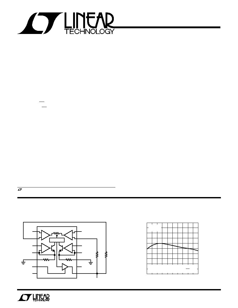
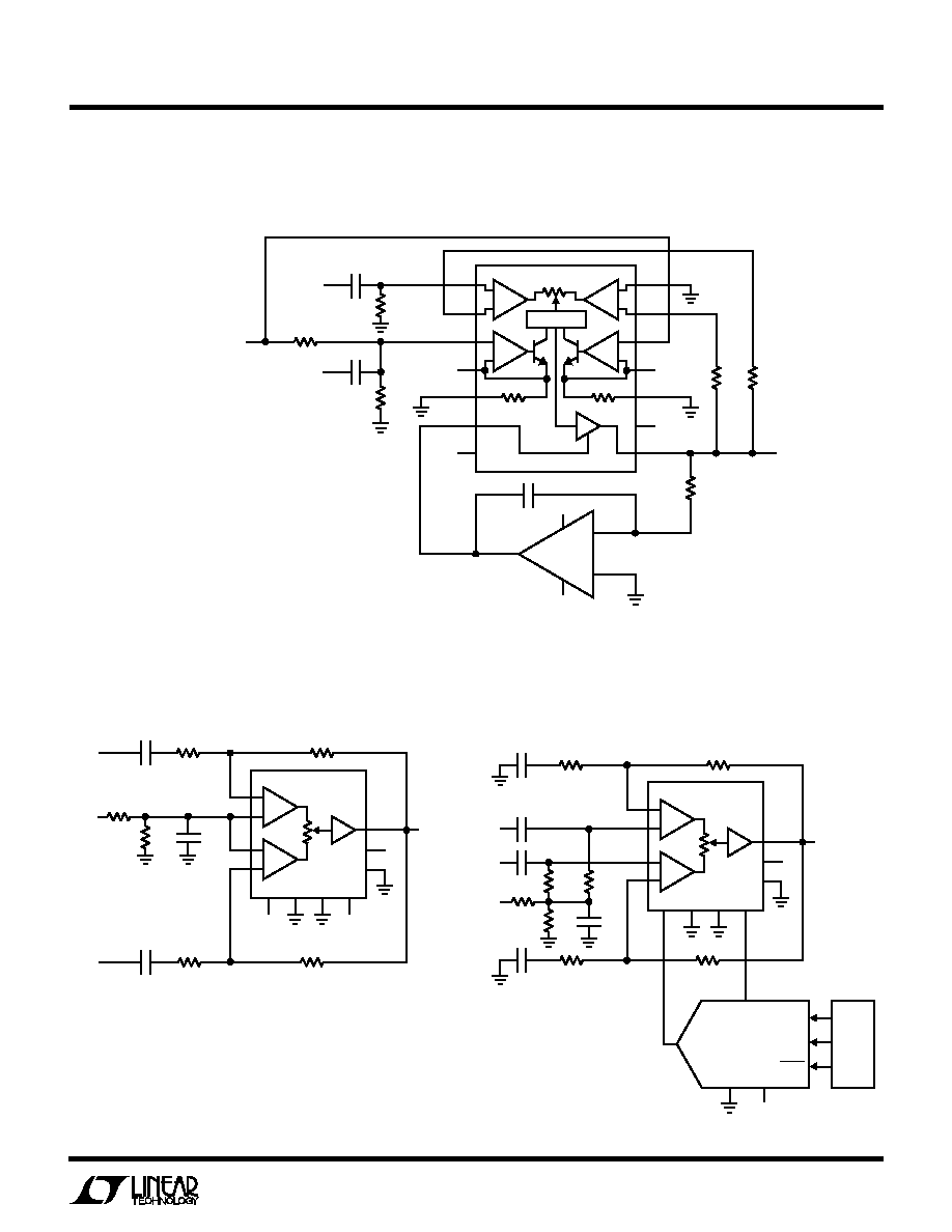
TYPICAL APPLICATIO
N
U
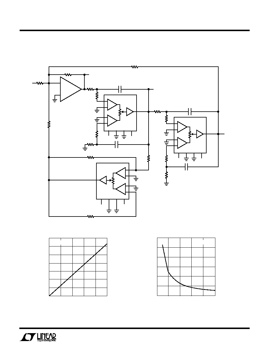
Two-Input Video Fader
≠
+
≠
+
IN1
IN2
2.5VDC
INPUT
R
F2
1.5k
V
OUT
R
F1
1.5k
I
FS
I
C
I
C
V
+
V
≠
NULL
1251/56 TA01
0V TO 2.5V
CONTROL
2
≠
+
≠
+
1
2
3
4
5
6
7
14
13
12
11
10
9
8
CONTROL
LT1251/LT1256
1
C
FS
5k
5k
I
FS
LT1256
Gain Accuracy vs Control Voltage
FEATURES
DESCRIPTIO
N
U
s
Accurate Linear Gain Control:
±
1% Typ,
±
3% Max
s
Constant Gain with Temperature
s
Wide Bandwidth: 40MHz
s
High Slew Rate: 300V/
µ
s
s
Fast Control Path: 10MHz
s
Low Control Feedthrough: 2.5mV
s
High Output Current: 40mA
s
Low Output Noise
45nV/
Hz at A
V
= 1
270nV/
Hz at A
V
= 100
s
Low Distortion: 0.01%
s
Wide Supply Range:
±
2.5V to
±
15V
s
Low Supply Current: 13mA
s
Low Differential Gain and Phase: 0.02%, 0.02
∞
, LTC and LT are registered trademarks of Linear Technology Corporation.
APPLICATIO
N
S
U
s
Composite Video Gain Control
s
RGB, YUV Video Gain Control
s
Video Faders, Keyers
s
Gamma Correction Amplifiers
s
Audio Gain Control, Faders
s
Multipliers, Modulators
s
Electronically Tunable Filters
The LT
Æ
1251/LT1256 are 2-input, 1-output, 40MHz cur-
rent feedback amplifiers with a linear control circuit that
sets the amount each input contributes to the output.
These parts make excellent electronically controlled vari-
able gain amplifiers, filters, mixers and faders. The only
external components required are the power supply by-
pass capacitors and the feedback resistors. Both parts
operate on supplies from
±
2.5V (or single 5V) to
±
15V
(or single 30V).
Absolute gain accuracy is trimmed at wafer sort to mini-
mize part-to-part variations. The circuit is completely
temperature compensated.
The LT1251 includes circuitry that eliminates the need for
accurate control signals around zero and full scale. For
control signals of less than 2% or greater than 98%, the
LT1251 sets one input completely off and the other
completely on. This is ideal for fader applications because
it eliminates off-channel feedthrough due to offset or gain
errors in the control signals.
The LT1256 does not have this on/off feature and operates
linearly over the complete control range. The LT1256 is
recommended for applications requiring more than 20dB
of linear control range.
CONTROL VOLTAGE (V)
0
GAIN ACCURACY (%)
5
4
3
2
1
0
≠1
≠2
≠3
≠4
≠5
2.0
1251/56 TA02
0.5
1.0
1.5
2.5
V
S
=
±
5V
V
FS
= 2.5V
100
GAIN ACCURACY (%) = A
VMEAS
≠
(
)
V
C
2.5
( )
2
LT1251/LT1256
ORDER PART
NUMBER
Total Supply Voltage (V
+
to V
≠
) .............................. 36V
Input Current ......................................................
±
15mA
Input Voltage on Pins 3,4,5,10,11,12 ............... V
≠
to V
+
Output Short-Circuit Duration (Note 1) ........ Continuous
Specified Temperature Range (Note 2) ....... 0
∞
C to 70
∞
C
Operating Temperature Range ............... ≠ 40
∞
C to 85
∞
C
Storage Temperature Range ................. ≠ 65
∞
C to 150
∞
C
Junction Temperature (Note 3)............................ 150
∞
C
Lead Temperature (Soldering, 10 sec).................. 300
∞
C
PACKAGE/ORDER I
N
FOR
M
ATIO
N
W
U
U
ABSOLUTE
M
AXI
M
U
M
RATINGS
W
W
W
U
LT1251CN
LT1251CS
LT1256CN
LT1256CS
T
JMAX
= 150
∞
C,
JA
= 70
∞
C/ W (N)
T
JMAX
= 150
∞
C,
JA
= 100
∞
C/ W (S)
Consult factory for Industrial and Military grade parts.
SIG AL A PLIFIER AC CHARACTERISTICS
U
W
0
∞
C
T
A
70
∞
C, V
S
=
±
5V, V
IN
= 1V
RMS
, f = 1kHz, A
VMAX
= 1, R
F1
= R
F2
= 1.5k, V
FS
= 2.5V, I
C
= I
FS
= NULL = Open, Pins 5,10 = GND,
unless otherwise noted.
(Note 2)
≠
+
≠
+
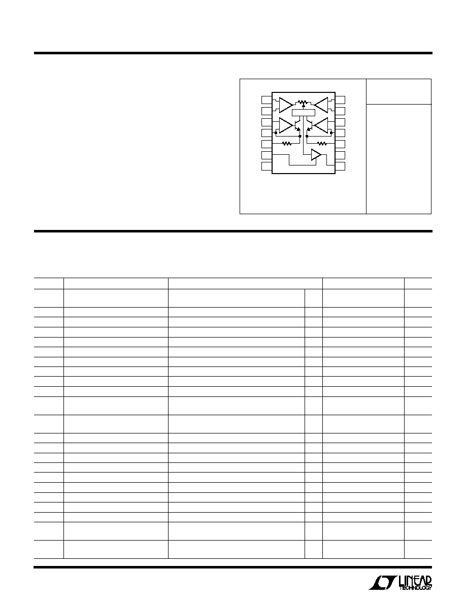
TOP VIEW
N PACKAGE
14-LEAD PDIP
S PACKAGE
14-LEAD PLASTIC SO
IN2
FB2
V
FS
I
FS
R
FS
V
+
V
OUT
2
≠
+
≠
+
1
2
3
4
5
6
7
IN1
FB1
V
C
I
C
R
C
NULL
V
≠
14
13
12
11
10
9
8
CONTROL
1
C
FS
SYMBOL
PARAMETER
CONDITIONS
MIN
TYP
MAX
UNITS
2%IN1
2% Input 1 Gain
V
C
(Pin 3) = 0.05V
LT1251
q
0
0.1
%
LT1256
q
0.1
5.0
%
10%IN1
10% Input 1 Gain
V
C
(Pin 3) = 0.25V
q
7
13
%
20%IN1
20% Input 1 Gain
V
C
(Pin 3) = 0.50V
q
17
23
%
30%IN1
30% Input 1 Gain
V
C
(Pin 3) = 0.75V
q
27
33
%
40%IN1
40% Input 1 Gain
V
C
(Pin 3) = 1.00V
q
37
43
%
50%IN1
50% Input 1 Gain
V
C
(Pin 3) = 1.25V
q
47
53
%
60%IN1
60% Input 1 Gain
V
C
(Pin 3) = 1.50V
q
57
63
%
70%IN1
70% Input 1 Gain
V
C
(Pin 3) = 1.75V
q
67
73
%
80%IN1
80% Input 1 Gain
V
C
(Pin 3) = 2.00V
q
77
83
%
90%IN1
90% Input 1 Gain
V
C
(Pin 3) = 2.25V
q
87
93
%
98%IN1
98% Input 1 Gain
V
C
(Pin 3) = 2.45V
LT1251
q
99.9
100.0
%
LT1256
q
95.0
99.9
%
2%IN2
2% Input 2 Gain
V
C
(Pin 3) = 2.45V
LT1251
q
0
0.1
%
LT1256
q
0.1
5.0
%
10%IN2
10% Input 2 Gain
V
C
(Pin 3) = 2.25V
q
7
13
%
20%IN2
20% Input 2 Gain
V
C
(Pin 3) = 2.00V
q
17
23
%
30%IN2
30% Input 2 Gain
V
C
(Pin 3) = 1.75V
q
27
33
%
40%IN2
40% Input 2 Gain
V
C
(Pin 3) = 1.50V
q
37
43
%
50%IN2
50% Input 2 Gain
V
C
(Pin 3) = 1.25V
q
47
53
%
60%IN2
60% Input 2 Gain
V
C
(Pin 3) = 1.00V
q
57
63
%
70%IN2
70% Input 2 Gain
V
C
(Pin 3) = 0.75V
q
67
73
%
80%IN2
80% Input 2 Gain
V
C
(Pin 3) = 0.50V
q
77
83
%
90%IN2
90% Input 2 Gain
V
C
(Pin 3) = 0.25V
q
87
93
%
98%IN2
98% Input 2 Gain
V
C
(Pin 3) = 0.05V
LT1251
q
99.9
100.0
%
LT1256
q
95.0
99.9
%
Gain Drift with Temperature
V
C
(Pin 3) = 0.75V
N Package
50
ppm/
∞
C
(Worst Case at 30% Gain)
V
C
(Pin 3) = 0.75V
S Package
400
ppm/
∞
C
3
LT1251/LT1256
SYMBOL
PARAMETER
CONDITIONS
MIN
TYP
MAX
UNITS
Gain Supply Rejection
V
C
= 1.25V, V
S
=
±
5V to
±
15V
q
0.03
0.10
%/V
External Resistor Gain
Pins 5,10 = Open, External 5k Resistors
q
45
55
%
50% Input 1
from Pins 4,11 to Ground, V
C
= 1.25V
SR
Slew Rate
V
IN
=
±
2.5V, V
O
at
±
2V, R
L
= 150
q
150
300
V/
µ
s
Control Feedthrough
V
C
= 1.25VDC + 2.5V
P-P
at 1kHz
2.5
mV
P-P
Full Power Bandwidth
V
O
= 1V
RMS
20
MHz
BW
Small-Signal Bandwidth
V
S
=
±
5V
30
MHz
V
S
=
±
15V
40
MHz
Differential Gain (Notes 4,5)
Control = 0% or 100%
0.02
%
Control = 25% or 75%
0.90
%
Differential Phase (Notes 4,5)
Control = 0% or 100%
0.02
DEG
Control = 25% or 75%
0.55
DEG
THD
Total Harmonic Distortion
Gain = 100%
0.002
%
Gain = 50%
0.015
%
Gain = 10%
0.4
%
t
r
, t
f
Rise Time, Fall Time
10% to 90%, V
O
= 100mV
11
ns
OS
Overshoot
V
O
= 100mV
3
%
t
PD
Propagation Delay
V
O
= 100mV
10
ns
t
S
Settling Time
0.1%,
V
O
= 2V
65
ns
SIG AL A PLIFIER AC CHARACTERISTICS
U
W
0
∞
C
T
A
70
∞
C, V
S
=
±
5V, V
IN
= 1V
RMS
, f = 1kHz, A
VMAX
= 1, R
F1
= R
F2
= 1.5k, V
FS
= 2.5V, I
C
= I
FS
= NULL = Open, Pins 5,10 = GND,
unless otherwise noted.
SIG AL A PLIFIER DC CHARACTERISTICS
U
W
0
∞
C
T
A
70
∞
C, V
S
=
±
5V, V
CM
= 0V, V
FS
= 2.5V, I
C
= I
FS
= NULL = Open, Pins 5,10 = GND, unless otherwise noted.
SYMBOL
PARAMETER
CONDITIONS
MIN
TYP
MAX
UNITS
V
OS
Input Offset Voltage
Either Input
q
2
5
mV
Difference Between Inputs
q
≠ 3
1
3
mV
Input Offset Voltage Drift
10
µ
V/
∞
C
I
IN
+
Noninverting Input Bias Current
Either Input
q
≠ 2.5
0.5
2.5
µ
A
I
IN
≠
Inverting Input Bias Current
Either Input
q
≠ 30
10
30
µ
A
Difference Between Inputs
q
≠ 1
0.5
1
µ
A
Inverting Input Bias Current Null Change
Null (Pin 6) Open to V
≠
q
≠ 280
≠ 170
≠ 60
µ
A
e
n
Input Noise Voltage Density
f = 1kHz
2.7
nV/
Hz
+i
n
Noninverting Input Noise Current Density
f = 1kHz
1.5
pA/
Hz
≠i
n
Inverting Input Noise Current Density
f = 1kHz
29
pA/
Hz
R
IN
Input Resistance
Either Noninverting Input
q
5
17
M
C
IN
Input Capacitance
Either Noninverting Input
q
1.5
pF
Input Voltage Range
V
S
=
±
5V
q
±
3
±
3.2
V
V
S
= 5V
q
2
3
V
CMRR
Common Mode Rejection Ratio
V
CM
= ≠ 3V to 3V
q
55
61
dB
V
S
= 5V, V
CM
= 2V to 3V, V
O
= 2.5V
q
50
57
dB
Inverting Input Current Common Mode Rejection
V
CM
= ≠ 3V to 3V
q
0.07
0.25
µ
A/ V
V
S
= 5V, V
CM
= 2V to 3V, V
O
= 2.5V
q
0.17
0.70
µ
A/ V
PSRR
Power Supply Rejection Ratio
V
S
=
±
5V to
±
15V
q
70
76
dB
Noninverting Input Current Power Supply Rejection
V
S
=
±
5V to
±
15V
q
30
100
nA/V
Inverting Input Current Power Supply Rejection
V
S
=
±
5V to
±
15V
q
30
200
nA/V
4
LT1251/LT1256
SIG AL A PLIFIER DC CHARACTERISTICS
U
W
0
∞
C
T
A
70
∞
C, V
S
=
±
5V, V
CM
= 0V, V
FS
= 2.5V, I
C
= I
FS
= NULL = Open, Pins 5,10 = GND, unless otherwise noted.
SYMBOL
PARAMETER
CONDITIONS
MIN
TYP
MAX
UNITS
A
VOL
Large-Signal Voltage Gain
V
O
= ≠ 3V to 3V, R
L
= 150
83
93
dB
V
O
= ≠ 2.75V to 2.75V, R
L
= 150
q
83
dB
R
OL
Transresistance,
V
OUT
/
I
IN
≠
V
O
= ≠ 3V to 3V, R
L
= 150
0.75
1.8
M
V
O
= ≠ 2.75V to 2.75V, R
L
= 150
q
0.75
M
V
OUT
Maximum Output Voltage Swing
No Load
q
±
4.0
±
4.2
V
R
L
= 150
±
3.0
±
3.5
V
q
±
2.75
V
V
S
=
±
15V, No Load
q
±
14.0
±
14.2
V
V
S
= 5V, V
CM
= 2.5V, (Note 6)
q
1.2
3.8
V
I
O
Maximum Output Current
V
S
=
±
5V
q
±
30
±
40
mA
V
S
= 5V, V
CM
= V
O
= 2.5V
q
±
20
±
30
mA
I
S
Supply Current
V
C
= V
FS
= 2.5V
q
13.5
17.0
mA
V
C
= V
FS
= 1.25V
q
7.5
9.5
mA
V
C
= V
FS
= 0V
q
1.3
1.8
mA
V
C
= V
FS
= 2.5V, V
S
=
±
15V
q
14.5
18.5
mA
V
C
= V
FS
= 0V, V
S
=
±
15V
q
1.4
2.0
mA
CO TROL A D FULL SCALE A PLIFIER CHARACTERISTICS
U
U
W
0
∞
C
T
A
70
∞
C, V
S
=
±
5V, V
FS
= 2.5V, I
C
= I
FS
= NULL = Open, Pins 5,10 = GND, unless otherwise noted.
SYMBOL
PARAMETER
CONDITIONS
MIN
TYP
MAX
UNITS
Control Amplifier Input Offset Voltage
Pin 4 to Pin 3
q
5
15
mV
Full-Scale Amplifier Input Offset Voltage
Pin 11 to Pin 12
q
5
15
mV
Control Amplifier Input Resistance
q
25
100
M
Full-Scale Amplifier Input Resistance
q
25
100
M
Control Amplifier Input Bias Current
q
≠ 750
≠ 300
nA
Full-Scale Amplifier Input Bias Current
q
≠ 750
≠ 300
nA
R
C
Internal Control Resistor
T
A
= 25
∞
C
3.75
5
6.25
k
R
FS
Internal Full-Scale Resistor
T
A
= 25
∞
C
4
5
6
k
Resistor Temperature Coefficient
0.2
%/
∞
C
Control Path Bandwidth
Small Signal, V
C
= 100mV, (Note 7)
10
MHz
Control Path Rise and Fall Time
Small Signal, V
C
= 100mV, (Note 7)
35
ns
Control Path Transition Time
0% to 100%
150
ns
Control Path Propagation Delay
Small Signal,
V
C
= 100mV
50
ns
V
C
from 0% or 100%
90
ns
The
q
denotes specifications which apply over the specified operating
temperature range.
Note 1: A heat sink may be required depending on the power supply
voltage.
Note 2: Commercial grade parts are designed to operate over the
temperature range of ≠ 40
∞
C to 85
∞
C but are neither tested nor guaranteed
beyond 0
∞
C to 70
∞
C. Industrial grade parts specified and tested over
≠ 40
∞
C to 85
∞
C are available on special request. Consult factory.
Note 3: T
J
is calculated from the ambient temperature T
A
and the power
dissipation P
D
according to the following formulas:
LT1251CN/LT1256CN:
T
J
= T
A
+ (P
D
∑ 70
∞
C/W)
LT1251CS/LT1256CS:
T
J
= T
A
+ (P
D
∑ 100
∞
C/W)
Note 4: Differential gain and phase are measured using a Tektronix
TSG120YC/NTSC signal generator and a Tektronix 1780R Video
Measurement Set. The resolution of this equipment is 0.1% and 0.1
∞
. Five
identical amplifier stages were cascaded giving an effective resolution of
0.02% and 0.02
∞
.
Note 5: Differential gain and phase are best when the control is set at 0%
or 100%. See the Typical Performance Characteristics curves.
Note 6: Tested with R
L
= 150
to 2.5V to simulate an AC coupled load.
Note 7: Small-signal control path response is measured driving R
C
(Pin 5)
to eliminate peaking caused by stray capacitance on Pin 4.
5
LT1251/LT1256
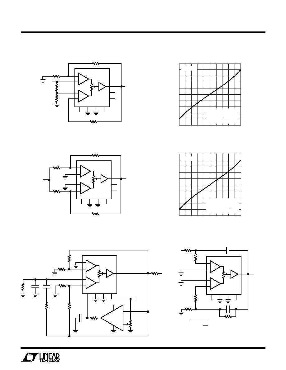
CONTROL VOLTAGE (V)
0
GAIN (V/
V)
1.0
0.8
0.6
0.4
0.2
0
2.0
1251/56 G01
0.5
1.0
1.5
2.5
V
FS
= 2.5V
IN2
IN1
TYPICAL PERFOR
M
A
N
CE CHARACTERISTICS
U
W
LT1251/LT1256
Control Path Bandwidth
FREQUENCY (Hz)
VOLTAGE GAIN (dB)
10
8
6
4
2
0
≠2
≠4
≠6
≠8
≠10
10k
1M
10M
100M
1251/56 G04
100k
VOLTAGE DRIVE V
C
V
S
= ±5V
PIN 4 NOT IN SOCKET
THD Plus Noise vs Frequency
FREQUENCY (Hz)
0.01
THD + NOISE (%)
0.1
1
10
10
1k
10k
1251/56 G08
0.001
100
100k
V
C
CC
= 10%
V
C
CC
= 50%
V
C
CC
= 100%
V
S
CC
= ±5V, V
IN
= 1V
RMS
A
V
= 1, R
F
= 1.5k, V
FS
= 2.5V
CONTROL VOLTAGE (V)
0
GAIN (V/
V)
1.0
0.8
0.6
0.4
0.2
0
2.0
1251/56 G02
0.5
1.0
1.5
2.5
V
FS
= 2.5V
IN2
IN1
FREQUENCY (Hz)
100k
OUTPUT VOLTAGE (V
P-P
)
8
7
6
5
4
3
2
1
1M
10M
100M
1251/56 G07
A
V
= 10
A
V
= 1
V
S
= ±5V
R
L
= 1k
R
F
= 1.5k
V
C
= V
FS
= 2.5V
Undistorted Output Voltage
vs Frequency
FREQUENCY (Hz)
VOLTAGE GAIN (dB)
10
8
6
4
2
0
≠2
≠4
≠6
≠8
≠10
10k
1M
10M
100M
1251/56 G05
100k
VOLTAGE DRIVE R
C
V
C
= GND
V
S
= ±5V
LT1251/LT1256
Control Path Bandwidth
FREQUENCY (MHz)
0
5
3RD ORDER INTERCEPT (dBm)
10
20
15
25
30
1251/56 G10
50
45
40
35
30
25
20
15
10
V
S
CC
= ±15V
A
V
= 1
R
F
= 1.5k
R
L
= 100
V
C
= V
FS
= 2.5V
3rd Order Intercept vs Frequency
2nd and 3rd Harmonic Distortion
vs Frequency
FREQUENCY (MHz)
1
DISTORTION (dBc)
≠20
≠30
≠40
≠50
≠60
≠70
10
100
1251/56 G09
V
S
CC
= ±5V
A
V
= 1
R
F
= 1.5k
R
L
= 1k
V
O
= 2V
P-P
V
C
= V
FS
= 2.5V
3RD
2ND
FREQUENCY (Hz)
10
1
10
100
100
1k
10k
1251/56 G06
SPOT NOISE (nV/
Hz OR pA/
Hz)
+i
n
e
n
≠i
n
Spot Input Noise Voltage and
Current vs Frequency
LT1251
Gain vs Control Voltage
LT1256
Gain vs Control Voltage
6
LT1251/LT1256
TYPICAL PERFOR
M
A
N
CE CHARACTERISTICS
U
W
FREQUENCY (Hz)
100k
VOLTAGE GAIN (dB)
PHASE SHIFT (DEG)
1M
10M
100M
1251/56 G13
5
4
3
2
1
0
≠1
≠2
≠3
≠4
≠5
45
0
≠45
≠90
≠135
≠180
≠225
≠270
V
S
= ±5V
R
F
= 1.3k
R
L
= 100
PHASE
GAIN
Voltage Gain and Phase
vs Frequency
Bandwidth vs Feedback
Resistance, A
V
= 1, R
L
= 1k
FEEDBACK RESISTANCE (k
)
0.6
≠
3dB BANDWIDTH (MHz)
70
60
50
40
30
20
10
0.8
1.0
1.2
1.4
1251/56 G12
1.6
1.8
PEAKING
0.5dB
PEAKING
5.0dB
V
S
= ±15V
V
S
= ±5V
V
S
= 5V
FEEDBACK RESISTANCE (k
)
0.6
≠
3dB BANDWIDTH (MHz)
70
60
50
40
30
20
10
0.8
1.0
1.2
1.4
1251/56 G11
1.6
1.8
PEAKING
0.5dB
PEAKING
5.0dB
V
S
= ±15V
V
S
= ±5V
V
S
= 5V
Bandwidth vs Feedback
Resistance, A
V
= 1, R
L
= 100
Bandwidth vs Feedback
Resistance, A
V
= 10, R
L
= 100
FEEDBACK RESISTANCE (k
)
0.4
≠
3dB BANDWIDTH (MHz)
60
50
40
30
20
10
0.6
0.8
1.0
1.2
1251/56 G14
1.4
1.6
PEAKING
0.5dB
PEAKING
5.0dB
V
S
= 5V
V
S
= ±15V
V
S
= ±5V
Bandwidth vs Feedback
Resistance, A
V
= 100, R
L
= 100
FEEDBACK RESISTANCE (k
)
0.2 0.4
≠3dB BANDWIDTH (MHz)
2.0
1251/56 G17
0.6 0.8 1.0
1.4
1.2
1.6 1.8
10
9
8
7
6
5
4
3
2
V
S
= ±15V
V
S
= 5V
V
S
= ±5V
NO PEAKING
Bandwidth vs Feedback
Resistance, A
V
= 10, R
L
= 1k
FEEDBACK RESISTANCE (k
)
0.4
≠
3dB BANDWIDTH (MHz)
60
50
40
30
20
10
0.6
0.8
1.0
1.2
1251/56 G15
1.4
1.6
PEAKING
0.5dB
PEAKING
5.0dB
V
S
= 5V
V
S
= ±15V
V
S
= ±5V
Bandwidth vs Feedback
Resistance, A
V
= 100, R
L
= 1k
FEEDBACK RESISTANCE (k
)
0.2 0.4
≠3dB BANDWIDTH (MHz)
2.0
1251/56 G18
0.6 0.8 1.0
1.4
1.2
1.6 1.8
10
9
8
7
6
5
4
3
2
V
S
= ±15V
V
S
= 5V
V
S
= ±5V
NO PEAKING
FREQUENCY (Hz)
OFF-CHANNEL ISOLATION (dB)
0
≠10
≠20
≠30
≠40
≠50
≠60
≠70
≠80
≠90
≠100
10k
1M
10M
100M
1251/56 G16
100k
V
S
= ±5V
V
FS
= 2.5V
V
C
= 0V
R
L
= 100
R
F
= 1.5k
A
V
= 10
A
V
= 1
Off-Channel Isolation
vs Frequency
≠3dB Bandwidth vs
Control Voltage
CONTROL VOLTAGE (V)
0
≠3dB BANDWIDTH (MHz)
40
35
30
25
20
15
10
0.5
1.0
1.5
2.0
1251/56 G19
2.5
V
S
= ±5V
R
L
= 100
V
FS
= 2.5V
R
F
= 1.3k
7
LT1251/LT1256
TYPICAL PERFOR
M
A
N
CE CHARACTERISTICS
U
W
Input Common Mode Range
vs Temperature
Control and Full-Scale Amp Input
Bias Current vs Input Voltage
NULL VOLTAGE, REFERENCED TO V
≠
(mV)
0
20
40
INVERTING INPUT BIAS CURRENT (
µ
A)
60
100 120
80
140 160
1251/56 G24
200
150
100
50
0
≠50
≠100
≠150
≠200
T
A
= ≠55∞C
T
A
= 125∞C
V
S
= ±5V
V
FS
= 1.25V
T
A
= 25∞C
Inverting Input Bias Current
vs Null Voltage
Inverting Input Bias Current
vs Null Voltage
NULL VOLTAGE, REFERENCED TO V
≠
(mV)
0
50
INVERTING INPUT BIAS CURRENT (
µ
A)
100
200
150
250
300
1251/56 G23
400
300
200
100
0
≠100
≠200
≠300
≠400
T
A
= ≠55∞C
T
A
= 125∞C
V
S
= ±5V
V
FS
= 2.5V
T
A
= 25∞C
Positive Output Saturation
Voltage vs Load Current
LOAD CURRENT (mA)
0
SATURATION VOLTAGE, V
+
≠ V
OUT
(V)
10
20
30
40
1251/56 G26
1.7
1.5
1.3
1.1
0.9
0.7
0.5
T
A
= ≠55∞C
T
A
= 125∞C
V
S
= ±5V
T
A
= 25∞C
Negative Output Saturation
Voltage vs Load Current
3.0
2.5
2.0
1.5
1.0
0.5
1251/56 G27
LOAD CURRENT (mA)
0
SATURATION VOLTAGE, V
OUT
≠ V
≠
(V)
≠10
≠20
≠30
≠40
T
A
= ≠55∞C
T
A
= 125∞C
V
S
= ±5V
T
A
= 25∞C
Output Short-Circuit Current
vs Temperature
TEMPERATURE (∞C)
≠50
OUTPUT SHORT-CIRCUIT CURRENT (mA)
60
50
40
30
25
75
1251/56 G28
≠25
0
50
100
125
Supply Current vs
Full-Scale Voltage
Supply Current vs
Full-Scale Current
INPUT VOLTAGE (V)
0
INPUT BIAS CURRENT (nA)
3
5
1251/56 G25
1
2
4
≠400
≠350
≠300
≠250
≠200
≠150
≠100
≠50
0
T
A
= ≠55∞C
T
A
= 125∞C
V
S
±7.5V
T
A
= 25∞C
FULL-SCALE VOLTAGE, V
FS
(V)
0
14
12
10
8
6
4
2
0
1.5
1251/56 G20
0.5
1.0
2.0
2.5
SUPPLY CURRENT (mA)
V
S
=
±
5V
INTERNAL RESISTORS
T
A
= ≠ 55
∞
C,
T
A
= 25
∞
C
T
A
= 125
∞
C
FULL-SCALE CURRENT, I
FS
(
µ
A)
0
SUPPLY CURRENT (mA)
14
12
10
8
6
4
2
0
1251/56 G21
200
500
100
300
400
V
S
=
±
5V
V
C
= 0V
T
A
= ≠ 55
∞
C
T
A
= 125
∞
C
TEMPERATURE (
∞
C)
≠50
≠25
COMMON MODE RANGE (V)
100
75
V
+
V
+
≠ 1
V
+
≠ 2
V
≠
+ 2
V
≠
+1
V
≠
1251/56 G22
0
25
50
125
8
LT1251/LT1256
TYPICAL PERFOR
M
A
N
CE CHARACTERISTICS
U
W
Slew Rate vs Temperature
Slew Rate vs Full-Scale
Reference Voltage
TEMPERATURE (∞C)
≠50
SLEW RATE (V/
µ
s)
100
1251/56 G30
0
50
350
300
250
200
≠25
25
75
125
V
S
= ±5V
A
V
= 1
NO LOAD
FREQUENCY (Hz)
1k
POWER SUPPLY REJECTION RATIO (dB)
80
70
60
50
40
30
20
10
0
100k
10k
1251/56 G31
1M
10M
V
S
= ±5V
A
V
= 1
R
F
= 1.5k
V
C
= V
FS
= 2.5V
POSITIVE
NEGATIVE
Power Supply Rejection Ratio
vs Frequency
Settling Time to 1mV
vs Output Step
Output Impedance vs Frequency
FREQUENCY (Hz)
OUTPUT IMPEDANCE (
)
100
10
1
0.1
0.01
10k
1M
10M
1251/56 G34
100k
100M
V
S
= ±5V
R
F
= 1.5k
V
C
= V
FS
= 2.5V
A
V
= 100
A
V
= 1, 10
SETTLING TIME (ns)
0
OUTPUT STEP (V)
25
50
75
100
1251/56 G32
125
10
8
6
4
2
0
≠2
≠4
≠6
≠8
≠10
150
V
S
= ±15V
R
F
= 1.5k
INVERTING,
NONINVERTING
INVERTING
NONINVERTING
Settling Time to 10mV
vs Output Step
SETTLING TIME (ns)
0
OUTPUT STEP (V)
50
100
1251/56 G33
150
10
8
6
4
2
0
≠2
≠4
≠6
≠8
≠10
200
INVERTING
INVERTING
NONINVERTING
NONINVERTING
V
S
= ±15V
R
F
= 1.5k
Differential Phase vs
Controlled Gain
Differential Gain vs
Controlled Gain
CONTROLLED GAIN, V
C
/V
FS
(%)
50
DIFFERENTIAL GAIN (%)
2
1
0
90
1251/56 G35
60
70
80
100
CONTROLLED GAIN, V
C
/V
FS
(%)
50
DIFFERENTIAL PHASE (DEG)
1.0
0.5
0
90
1251/56 G36
60
70
80
100
LT1251
Switching Transient (Glitch)
50mV
0
≠ 50mV
2.5
0
V
FS
= 2.5V
R
F1
= R
F2
= 1.5k
V
S
=
±
5V
1251/56 G37
V
C
V
OUT
FULL-SCALE REFERENCE VOLTAGE (V)
0
350
300
250
200
150
100
50
0
1.5
1251/56 G29
0.5
1.0
2.0
2.5
SLEW RATE (V/
µ
s)
A
V
= 1
V
S
=
±
15V
V
S
=
±
5V
9
LT1251/LT1256
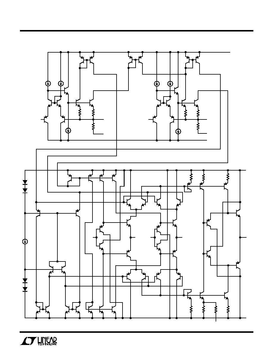
SI PLIFIED SCHE ATIC
W
W
+
+
+
I
4
I
5
I
3
1251/56 SS
Q5
Q16
Q17
Q6
R1
250
Q7
Q2
Q1
R2
250
R3
250
R4
250
R5
200
R6
200
R7
200
R11
200
R9
200
R8
200
R10
400
R
C
5k
R
FS
5k
I
C
V
FS
R
C
R
FS
I
FS
V
C
Q8
Q9
Q19
Q20
Q21
Q22
Q12
Q13
Q23
Q24
Q25
Q26
Q27
Q28
Q33
Q34
Q35
Q40
Q41
Q44
Q45
Q47
Q46
Q43
Q42
IN1
FB1
FB2
Q15
Q14
Q3
Q4
Q18
Q29
Q30
Q31
Q32
Q36 Q37
Q38
Q39
Q52
Q53
Q56
V
CC
V
CC
D1
NULL
V
EE
V
EE
OUT
Q55
Q57
Q58
Q61
Q60
Q59
IN2
Q48 Q49
Q50
Q51
+
I
1
+
I
2
Q54
+
I
6
Q10
Q11
D2
D3
D4
I
7

10
LT1251/LT1256
APPLICATIO
N
S I
N
FOR
M
ATIO
N
W
U
U
U
Supply Voltage
The LT1251/LT1256 are high speed amplifiers. To prevent
problems, use a ground plane with point-to-point wiring
and small bypass capacitors (0.01
µ
F to 0.1
µ
F) at each
supply pin. For good settling characteristics, especially
driving heavy loads, a 4.7
µ
F tantalum within an inch or two
of each supply pin is recommended.
The LT1251/LT1256 can be operated on single or split
supplies. The minimum total supply is 4V (Pins 7 to 9).
However, the input common mode range is only guaran-
teed to within 2V of each supply. On a 4V supply the parts
must be operated in the inverting mode with the noninvert-
ing input biased half way between Pin 7 and Pin 9. See the
Typical Applications section for the proper biasing for
single supply operation.
The op amps in the control section operate from V
≠
(Pin 7) to within 2V of V
+
(Pin 9). For this reason the
positive supply should be 4.5V or greater in order to use
2.5V control and full-scale voltages.
Inputs
The noninverting inputs (Pins 1 and 14) are easy to drive
since they look like a 17M resistor in parallel with a 1.5pF
capacitor at most frequencies. However, the input stage
can oscillate at very high frequencies (100MHz to 200MHz)
if the source impedance is inductive (like an unterminated
cable). Several inches of wire look inductive at these high
frequencies and can cause oscillations. Check for oscilla-
tions at the inverting inputs (Pins 2 and 13) with a 10
◊
probe and a 200MHz oscilloscope. A small capacitor
(10pF to 50pF) from the input to ground or a small resistor
(100
to 300
) in series with the input will stop these
parasitic oscillations, even when the source is inductive.
These components must be within an inch of the IC in
order to be effective.
All of the inputs to the LT1251/LT1256 have ESD protec-
tion circuits. During normal operation these circuits have
no effect. If the voltage between the noninverting and
inverting inputs exceeds 6V, the protection circuits will
trigger and attempt to short the inputs together. This
condition will continue until the voltage drops to less than
500mV or the current to less than 10mA. If a very fast edge
is used to measure settling time with an input step of more
than 6V, the protection circuits will cause the 1mV settling
time to become hundreds of microseconds.
Feedback Resistor Selection
The feedback resistor value determines the bandwidth of
the LT1251/LT1256 as in other current feedback amplifi-
ers. The curves in the Typical Performance Characteristics
show the effect of the feedback resistor on small-signal
bandwidth for various loads, gains and supply voltages.
The bandwidth is limited at high gains by the 500MHz to
800MHz gain-bandwidth product as shown in the curves.
Capacitance on the inverting input will cause peaking and
increase the bandwidth. Take care to minimize the stray
capacitance on Pins 2 and 13 during printed circuit board
layout for flat response.
If the two input stages are not operating with equal gain,
the gain versus control voltage characteristic will be
nonlinear. This is true even if R
F1
equals R
F2
. This is
because the open-loop characteristic of a current feed-
back amplifier is dependent on the Thevenin impedance at
the inverting input. For linear control of the gain, the loop
gain of the two stages must be equal. For an extreme
example, let's take a gain of 101 on input 1, R
F1
= 1.5k and
R
G1
= 15
, and unity-gain on input 2, R
F2
= 1.5k. The curve
in Figure 1 shows about 25% error at midscale. To
eliminate this nonlinearity we must change the value of
R
F2
. The correct value is the Thevenin impedance at
inverting input 1 (including the internal resistance of 27
)
times the gain set at input 1. For a linear gain versus
control voltage characteristic when input 2 is operating at
unity-gain, the formula is:
R
F2
= (A
V1
)(R
F1
R
G1
+ 27)
R
F2
= (101)(14.85 + 27) = 4227
Because the feedback resistor of the unity-gain input is
increased, the bandwidth will be lower and the output
noise will be higher. We can improve this situation by
reducing the values of R
F1
and R
G1
, but at high gains the
internal 27
dominates.
11
LT1251/LT1256
APPLICATIO
N
S I
N
FOR
M
ATIO
N
W
U
U
U
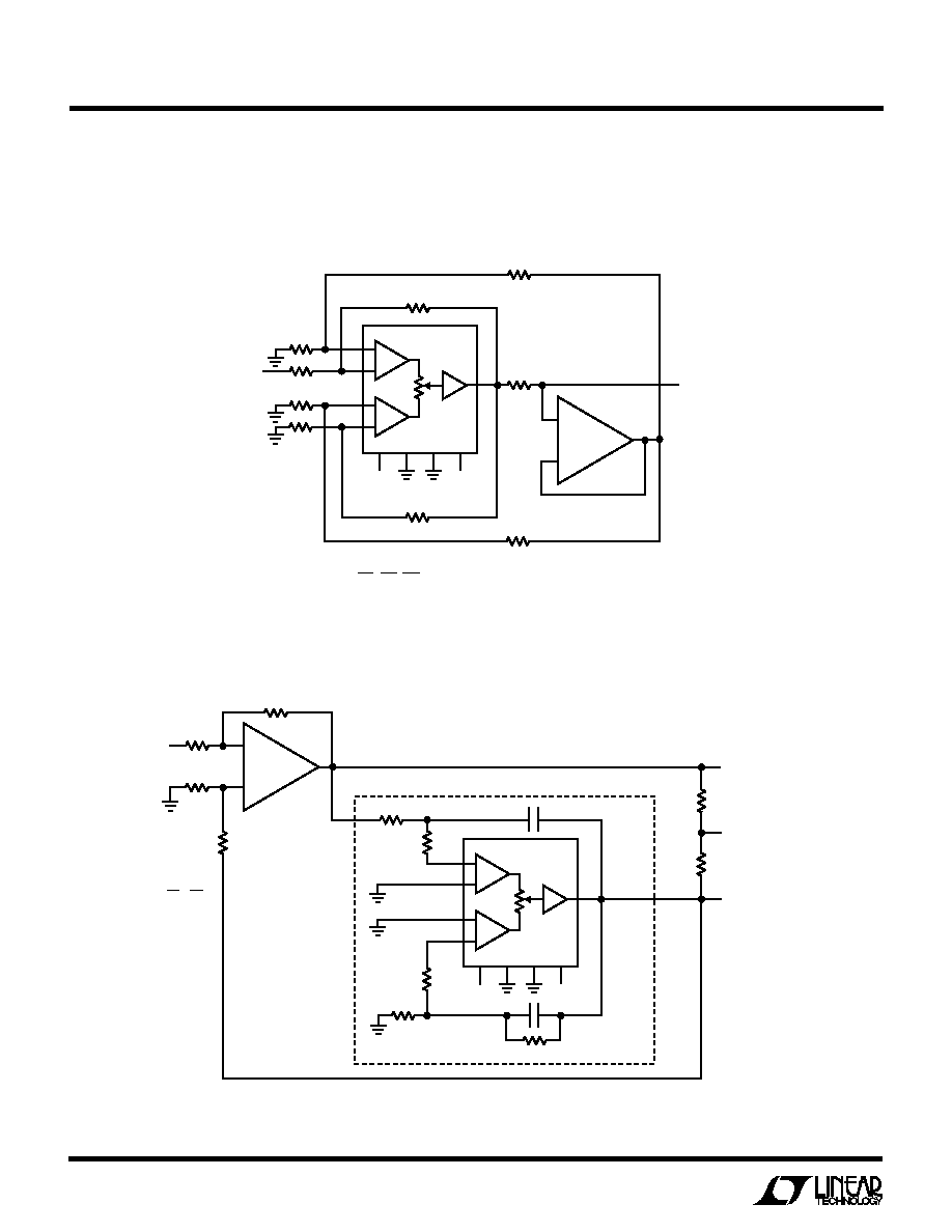
Capacitive Loads
Increasing the value of the feedback resistor reduces the
bandwidth and open-loop gain of the LT1251/LT1256;
therefore, the pole introduced by a capacitive load can be
overcome. If there is little or no resistive load in parallel
with the load capacitance, the output stage will resonate,
peak and possibly oscillate. With a resistive load of 150
,
any capacitive load can be accommodated by increasing
the feedback resistor. If the capacitive load cannot be
paralleled with a DC load of 150
, a network of 200pF in
series with 100
should be placed from the output to
ground. Then the feedback resistor should be selected for
best response.
The Null Pin
Pin 6 can be used to adjust the gain of an internal current
mirror to change the output offset. The open circuit
voltage at Pin 6 is set by the full scale current I
FS
flowing
through 200
to the negative supply. Therefore, the NULL
pin sits 100mV above the negative supply with V
FS
equal
to 2.5V. Any op amp whose output swings within a few
millivolts of the negative supply can drive the NULL pin.
The AM modulator application shows an LT1077 driving
the NULL pin to eliminate the output DC offset voltage.
Crosstalk
The amount of signal from the off input that appears at the
output is a function of frequency and the circuit topology.
The nature of a current feedback input stage is to force the
voltage at the inverting input to be equal to the voltage at
the noninverting input. This is independent of feedback
and forced by a buffer amplifier between the inputs. When
the LT1251/LT1256 are operating noninverting, the off
input signal is present at the inverting input. Since one end
of the feedback resistor is connected to this input, the off
signal is only a feedback resistor away from the output.
The amount of unwanted signal at the output is deter-
mined by the size of the feedback resistor and the output
impedance of the LT1251/LT1256. The output impedance
rises with increasing frequency resulting in more crosstalk
at higher frequencies. Additionally, the current that flows
in the inverting input is diverted to the supplies within the
chip and some of this signal will also show up at the
output. With a 1.5k feedback resistor, the crosstalk is
down about 86dB at low frequencies and rises to ≠ 78dB
at 1MHz and on to ≠ 60dB at 6MHz. The curves show the
details.
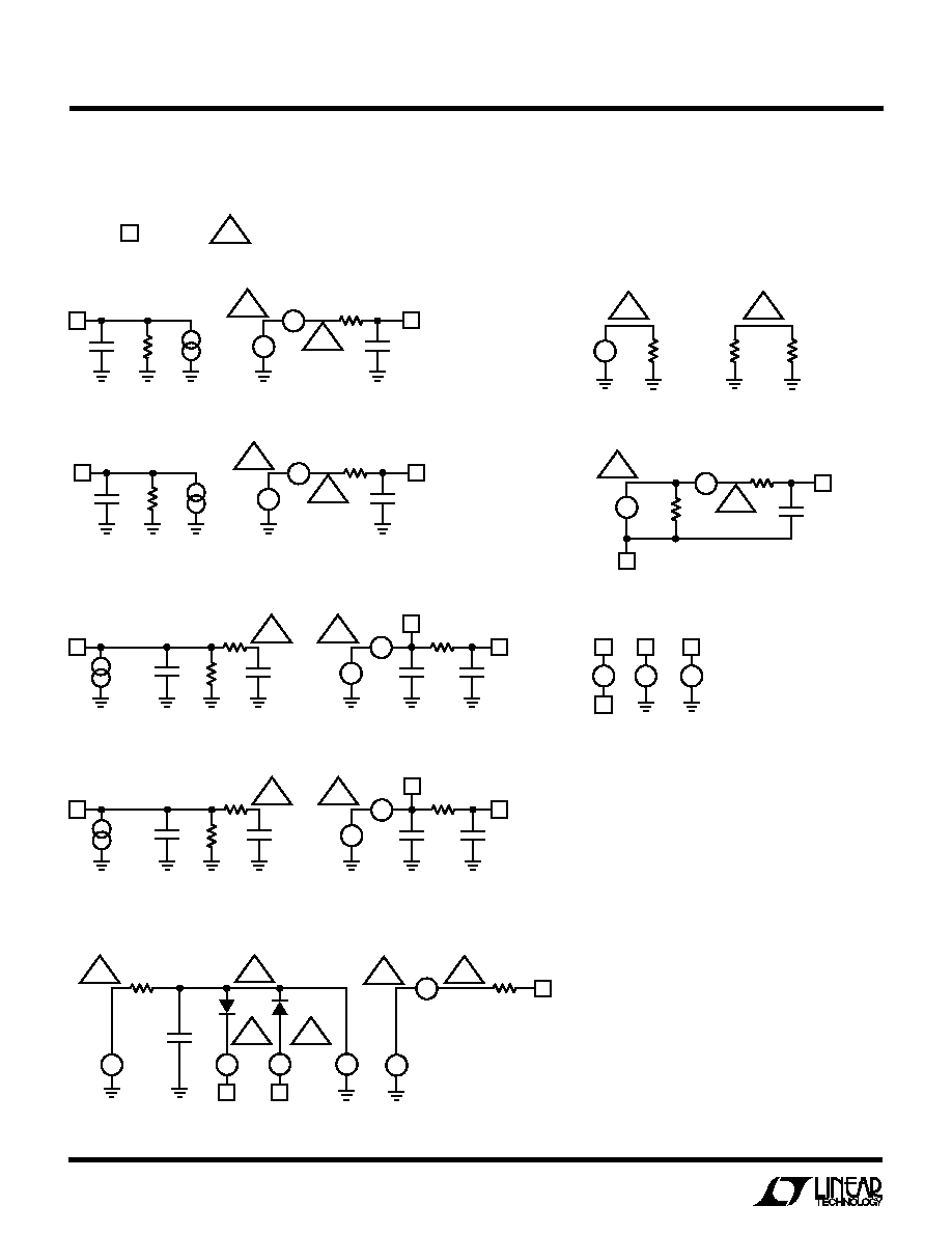
Distortion
When only one input is contributing to the output (V
C
= 0%
or 100%) the LT1251/LT1256 have very low distortion. As
the control reduces the output, the distortion will increase.
The amount of increase is a function of the current that
flows in the inverting input. Larger input signals generate
more distortion. Using a larger feedback resistor will
reduce the distortion at the expense of higher output
noise.
CONTROL VOLTAGE (V)
0
GAIN (V/
V)
100
50
0
2.0
1251/56 F01
0.5
1.0
1.5
2.5
R
F2
= 4.3k
R
F2
= 1.5k
V
FS
= 2.5V
Figure 1. Linear Gain Control from 0 to 101
12
LT1251/LT1256
APPLICATIO
N
S I
N
FOR
M
ATIO
N
W
U
U
U
Figure 2 is the basic block diagram of the LT1251/LT1256
signal path with external resistors R
G1
, R
F1
, R
G2
and R
F2
.
Both input stages are operating as noninverting amplifiers
with two input signals V
1
and V
2
.
Each input stage has a unity-gain buffer from the nonin-
verting input to the inverting input. Therefore, the inverting
input is at the same voltage as the noninverting input. R
1
and R
2
represent the internal output resistances of these
buffers, approximately 27
.
K is a constant determined by the control circuit and can
be any value between 0 and 1. The control circuit is
described in a later section.
By inspection of the diagram:
I
V
R
R
R
R
R
V
R
R
R
R
G
F
G
F
O
F
F
G
1
1
1
1
1
1
1
1
1
1
1
1
=
+
( )( )
+
-
+
+
Substituting and rearranging gives:
I
V
R
R
R
R
R
V
R
R
R
R
I
KI
K I
V
I
R
sR C
G
F
G
F
O
F
F
G
O
O
O
OL
OL
2
2
2
2
2
2
2
2
2
2
2
1
2
1
1
1
=
+
( )( )
+
-
+
+
=
+ -
( )
=
+
(
)
General Equation for the Noninverting Amplifier Case
V
KV
R
R
R
R
R
K V
R
R
R
R
R
sR C
R
K
R
R
R
R
K
R
R
R
R
O
G
F
G
F
G
F
G
F
OL
OL
F
F
G
F
F
G
=
+
( )( )
+
+
-
( )
+
( )( )
+
+
+
+
+
+
-
( )
+
+
1
1
1
1
1
1
2
2
2
2
2
2
1
1
1
1
2
2
2
2
1
1
1
1
1
≠
+
1
14
K
I
1
I
O
8
C
V
O
1251/56 BD
I
1
I
2
I
2
1 ≠ K
R
1
V
1
V
2
R
2
R
G2
R
G1
R
OL
R
F1
R
F2
2
13
+1
≠
+
1
2
Figure 2. Signal Path Block Diagram
Signal Path Description

13
LT1251/LT1256
APPLICATIO
N
S I
N
FOR
M
ATIO
N
W
U
U
U
In low gain applications, R
1
and R
2
are small compared to
the feedback resistors and therefore we can simplify the
equation to:
V
KV
R
R
R
R
K V
R
R
R
R
sR C
R
K
R
K
R
O
G
F
G
F
G
F
G
F
OL
OL
F
F
=
( )( )
+
+
-
( )
( )( )
+
+
+
+
-
( )
1
1
1
1
1
2
2
2
2
2
1
2
1
1
1
Note that the denominator causes a gain error due to the
open-loop gain (typically 0.1% for frequencies below
20kHz) and for mismatches in R
F1
and R
F2
. A 1% mis-
match in the feedback resistors results in a 0.25% error at
K = 0.5.
If we set R
F1
= R
F2
and assume R
OL
>> R
F1
(a 0.1% error
at low frequencies) the above equation simplifies to:
and
V
KV A
K V A
where A
R
R
A
R
R
O
V
V
V
F
G
V
F
G
=
+ -
( )
= +
= +
1
1
2
2
1
1
1
2
2
2
1
1
1
This shows that the output fades linearly from input 2,
times its gain, to input 1, times its gain, as K goes from
0 to 1.
If only one input is used (for example, V
1
) and Pin 14 is
grounded, then the gain is proportional to K.
V
V
KA
O
V
1
1
=
Similarly for the inverting case where the noninverting
inputs are grounded and the input voltages V
1
and V
2
drive
the normally grounded ends of R
G1
and R
G2
, we get:
General Equation for the Inverting Amplifier Case
V
KV
R
R
R
R
K V
R
R
R
R
sR C
R
K
R
R
R
R
K
R
R
R
R
O
G
G
F
G
G
F
OL
OL
F
F
G
F
F
G
= -
+
+
+
-
( )
+
+
+
+
+
+
+
-
( )
+
+
1
1
1
1
1
2
2
2
2
2
1
1
1
1
2
2
2
2
1
1
1
1
1
1
1
Note that the denominator is the same as the noninverting
case. In low gain applications, R
1
and R
2
are small
compared to the feedback resistors and therefore we can
simplify the equation to:
V
KV
R
K V
R
sR C
R
K
R
K
R
O
G
G
OL
OL
F
F
= -
+
-
( )
+
+
+
-
( )
1
1
2
2
1
2
1
1
1
Again, if we set R
F1
= R
F2
and assume R
OL
>> R
F1
(a 0.1%
error at low frequencies) the above equation simplifies to:
and
V
KV A
K V A
where A
R
R
A
R
R
O
V
V
V
F
G
V
F
G
= -
+ -
( )
[
]
=
=
1
1
2
2
1
1
1
2
2
2
1
The 4-resistor difference amplifier yields the same result
as the inverting amplifier case, and the common mode
rejection is independent of K.
14
LT1251/LT1256
APPLICATIO
N
S I
N
FOR
M
ATIO
N
W
U
U
U
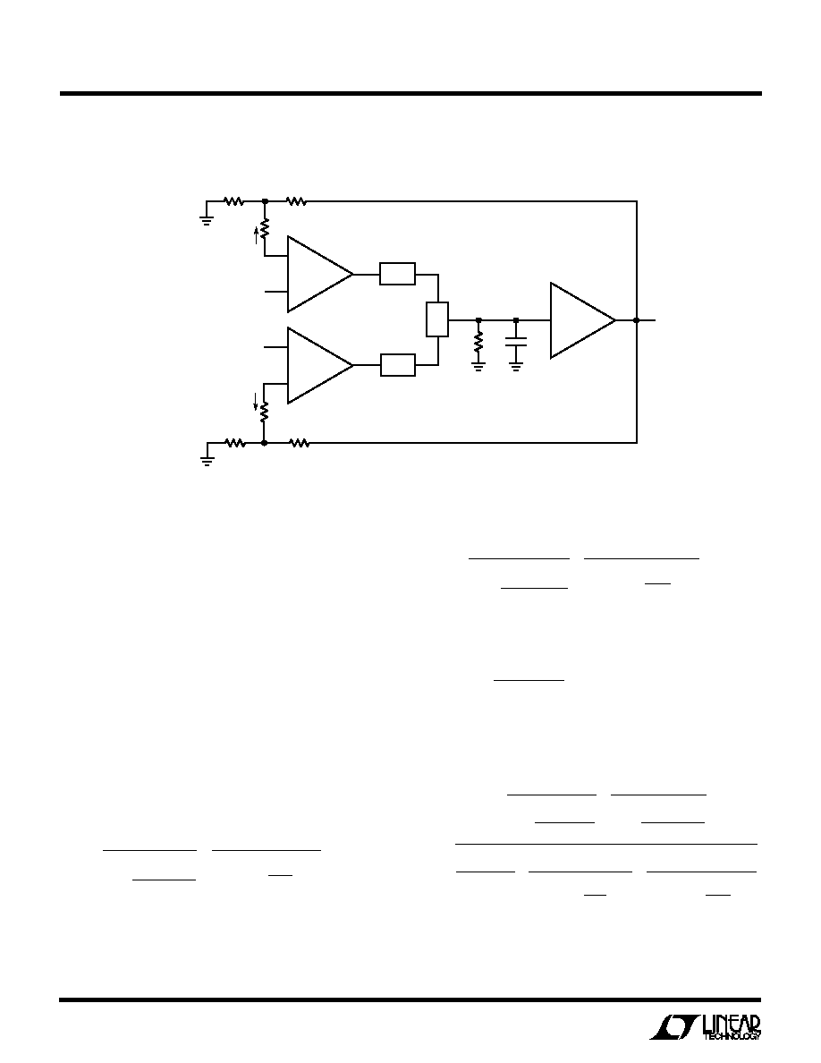
Control Circuit Description
1251/56 F03
I
FS
I
C
I
C
V
C
V
FS
I
FS
R
FS
V
+
R
C
3
5
12
11
10
4
≠
+
≠
+
CONTROL V TO I
FULL SCALE V TO I
C
FS
R
FS
5k
R
C
5k
gain) is
±
3% as detailed in the electrical tables. By using
a 2.5V full-scale voltage and the internal resistors, no
additional errors need be accounted for.
In the LT1256, K changes linearly with I
C
. To insure that K
is zero, V
C
must be negative 15mV or more to overcome
the worst-case control op amp offset. Similarly to insure
that K is 100%, V
C
must be 3% larger than V
FS
based on
the guaranteed gain accuracy.
To eliminate the overdrive requirement, the LT1251 has
internal circuitry that senses when the control current is at
about 5% and sets K to 0%. Similarly, at about 95% it sets
K to 100%. The LT1251 guarantees that a 2% (50mV)
input gives zero and 98% (2.45V) gives 100%.
The operating currents of the LT1251/LT1256 are derived
from I
FS
and therefore the quiescent current is a function
of V
FS
and R
FS
. The electrical tables show the supply
current for three values of V
FS
including zero. An approxi-
mate formula for the supply current is:
I
S
= 1mA + (24)(I
FS
) + (V
S
/20k)
where V
S
is the total supply voltage between Pins 9 and 7.
By reducing I
FS
the supply current can be reduced, how-
ever, the slew rate and bandwidth will also be reduced as
indicated in the characteristic curves. Using the internal
resistors (5k) with V
FS
equal to 2.5V results in I
FS
equal to
500
µ
A; there is no reason to use a larger value of I
FS
.
The inverting inputs of the V-to-I converters are available
so that external resistors can be used instead of the
internal ones. For example, if a 10V full-scale voltage is
desired, an external pair of 20k resistors should be used to
set I
FS
to 500
µ
A. The positive supply voltage must be 2.5V
greater than the maximum V
C
and/or V
FS
to keep the
transistors from saturating. Do not use the internal resis-
tors with external resistors because the internal resistors
have a large positive temperature coefficient (0.2%/
∞
C)
that will cause gain errors.
If the control voltage is applied to the free end of resistor
R
C
(Pin 5) and the V
C
input (Pin 3) is grounded, the polarity
of the control voltage must be inverted. Therefore, K will
be 0% for zero input and 100% for ≠ 2.5V input, assuming
V
FS
equals 2.5V. With Pin 3 grounded, Pin 4 is a virtual
ground; this is convenient for summing several negative
going control signals.
The control section of the LT1251/LT1256 consists of two
identical voltage-to-current converters (V-to-I); each
V-to-I contains an op amp, an NPN transistor and a
resistor. The converter on the right generates a
full-scale
current I
FS
and the one on the left generates a
control
current I
C
. The ratio I
C
/I
FS
is called K. K goes from a
minimum of zero (when I
C
is zero) to a maximum of one
(when I
C
is equal to, or greater than, I
FS
). K determines the
gain from each signal input to the output.
The op amp in each V-to-I drives the transistor until the
voltage at the inverting input is the same as the voltage at
the noninverting input. If the open end of the resistor (Pin
5 or 10) is grounded, the voltage across the resistor is the
same as the voltage at the noninverting input. The emitter
current is therefore equal to the input voltage V
C
divided by
the resistor value R
C
. The collector current is essentially
the same as the emitter current and it is the ratio of the two
collector currents that sets the gain.
The LT1251/LT1256 are tested with Pins 5 and 10 grounded
and a full-scale voltage of 2.5V applied to V
FS
(Pin 12). This
sets I
FS
at approximately 500
µ
A; the control voltage V
C
is
applied to Pin 3. When the control voltage is negative or
zero, I
C
is zero and K is zero. When V
C
is 2.5V or greater,
I
C
is equal to or greater than I
FS
and K is one. The gain of
channel one goes from 0% to 100% as V
C
goes from zero
to 2.5V. The gain of channel two goes the opposite way,
from 100% down to 0%. The worst-case error in K (the
Figure 3. Control Circuit Block Diagram
15
LT1251/LT1256
≠
+
≠
+
1MHz
CARRIER
AUDIO
MODULATION
2.5VDC
INPUT
50
R
F2
1.5k
V
OUT
R
F1
1.5k
I
C
V
+
V
+
V
≠
V
≠
NULL
1251/56 TA03
2
≠
+
≠
+
1
2
3
4
5
6
7
14
13
12
11
10
9
8
CONTROL
LT1256
1
C
0.1
µ
F
220k
220k
220k
FS
5k
5k
I
FS
0.1
µ
F
0.1
µ
F
≠
+
LT1077
AM Modulator with DC Output Nulling Circuit
TYPICAL APPLICATIO
N
S
U
10k
10k
5V
R
F1
1.5k
R
F2
1.5k
R
G2
1.5k
R
G1
1.5k
V1
V2
1251/56 TA06
2
8
9
14
13
7
12
10
5
3
1
10
µ
F
10
µ
F
10
µ
F
10
µ
F
5V
5V
20k
20k
+
+
10
µ
F
µ
P
V
C
R
C
R
FS
V
FS
V
+
V
≠
≠
+
≠
+
LT1251/LT1256
1
2
V
REF
V
OUT
V
OUT
LTC1257
GND
V
CC
D
IN
CLK
LOAD
+
+
+
Single Supply Noninverting AC Amplifier
with Digital Gain Control
Single Supply Inverting AC Amplifier
R2
20k
R1
20k
R
F1
1.5k
R
F2
1.5k
R
G1
1.5k
R
G2
1.5k
V
+
V1
V2
1251/56 TA05
2
8
9
14
13
7
12
10
5
3
1
C1
10
µ
F
5V
V
OUT
2.5VDC
INPUT
CONTROL
VOLTAGE
C
O
10
µ
F
+
C2
10
µ
F
+
V
C
R
C
R
FS
V
FS
V
+
V
≠
≠
+
LT1251/LT1256
2
≠
+
1
+
16
LT1251/LT1256
TYPICAL APPLICATIO
N
S
U
Controlled Gain, Voltage-to-Current Converter
(Current Source)
R
F
1k
R
F
1k
R
F
1k
OUTPUT RESISTANCE DEPENDS
ON MATCHING OF RESISTORS
R
F
1k
R
G
100
◊ 4
V
IN
1251/56 TA09
2
8
14
13
12
10
5
3
1
I
OUT
V
C
R
C
R
FS
V
FS
LT1256
≠
+
≠
+
2
1
R
O
1k
≠
+
LT1363
I
OUT
=
( )
V
IN
R
O
R
F
R
G
V
C
V
FS
2.5VDC
INPUT
CONTROL
VOLTAGE
R1
R3
V
IN
1251/56 TA13
R
R
INVERTED
HIGHPASS
ALLPASS
LOWPASS
R4
R2
≠
+
LT1252
BASIC VARIABLE INTEGRATOR
1.5k
2
8
C
C
14
13
12
10
5
3
1
V
C
V
C
R
C
R
FS
V
FS
V
FS
LT1256
≠
+
≠
+
2
1
1.5k
R
R
R
DC
10k
R1
R2
R3
R4
=
Variable Lowpass, Highpass and Allpass Filter
17
LT1251/LT1256
TYPICAL APPLICATIO
N
S
U
Logarithmic Gain Control (Noninverting)
Logarithmic Gain Control (Inverting)
1k
200
200
100pF
100pF
50
1251/56 TA11
2
8
7
5, 4, 6
5V
10
µ
F
2.5VDC
INPUT
V
OUT
14
13
12
10
5
3
1
V
C
R
C
R
FS
V
FS
LT1251/LT1256
≠
+
≠
+
2
1
1k
10k
1k
1
2
3
1.6k
1.6k
≠
+
LT1116
+
1.5k
1251/56 TA12
2
8
V
IN
V
OUT
C
C
THE TIME CONSTANT IS INVERSELY PROPORTIONAL TO V
C
.
R
DC
IS REQUIRED TO DEFINE THE DC OUTPUT WHEN
THE CONTROL IS AT ZERO.
14
13
12
10
5
3
1
V
C
V
C
R
C
R
FS
V
FS
V
FS
LT1256
≠
+
≠
+
2
1
1.5k
R
R
R
DC
10k
T(s) =
≠1
(s)(R)(C)
V
FS
V
C
( )
1MHz Wien Bridge Oscillator
Basic Variable Integrator
600
200
2k
6k
1.5k
V
IN
1251/56 TA07a
2
8
14
13
12
10
5
3
1
V
OUT
2.5VDC
INPUT
V
C
CONTROL
VOLTAGE
R
C
R
FS
V
FS
9
7
V
+
V
≠
LT1251/LT1256
≠
+
≠
+
2
1
6k
6k
1.5k
1.5k
V
IN
1251/56 TA08a
2
8
9
14
13
7
12
10
5
3
1
V
OUT
2.5VDC
INPUT
V
C
CONTROL
VOLTAGE
R
C
R
FS
V
FS
V
+
V
≠
LT1251/LT1256
≠
+
≠
+
2
1
CONTROL VOLTAGE (V)
0
GAIN (dB)
15
0
≠15
1251/56 TA07b
1.25
2.5
V
FS
= 2.5V
A
V
= 24dB
≠ 0.5
( )
V
C
V
FS
<1dB ERROR
CONTROL VOLTAGE (V)
0
GAIN (dB)
15
0
≠15
1251/56 TA08b
1.25
2.5
V
FS
= 2.5V
A
V
= 24dB
≠ 0.5
( )
V
C
V
FS
<1dB ERROR
18
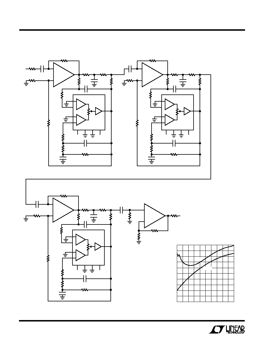
LT1251/LT1256
TYPICAL APPLICATIO
N
S
U
R9
1.5k
1251/56 TA14a
2
8
V
IN
C2
100pF
C5
50pF
C1
0.001
µ
F
14
13
12
2.5V
10
5
3
1
V
C
V
C
R
C
R
FS
V
FS
LT1256
≠
+
≠
+
2
1
R7
150
R8
910
R10
1.5k
R4
1k
R11
150
R2
1k
R1
470
R5
430
R6
430
R3
470
C3, 100pF
C4
0.002
µ
F
R12, 10k
≠
+
1/2
LT1253
C
'
1
0.001
µ
F
R
'
9
1.5k
2
8
C
'
2
100pF
C
'
5
50pF
14
13
12
2.5V
10
5
3
1
V
C
V
C
R
C
R
FS
V
FS
LT1256
≠
+
≠
+
2
1
R
'
7
150
R
'
8
910
R
'
10
1.5k
R
'
4
1k
R
'
11
150
R
'
2
1k
R
'
5
430
R
'
6
430
R
'
3
470
C
'
3, 100pF
C
'
4
0.002
µ
F
R
'
12, 10k
≠
+
1/2
LT1253
C
''
1
0.001
µ
F
R
''
9
1.5k
2
8
C
''
2
100pF
C
''
5
50pF
14
13
12
2.5V
10
5
3
1
V
C
V
C
R
C
R
FS
V
FS
LT1256
≠
+
≠
+
2
1
R
''
7
150
R
''
8
910
R
''
10
1.5k
R
''
4
1k
R
''
11
150
75
V
OUT
1k
10k
R
''
2
1k
R
''
5
430
R
''
6
430
R
''
3
470
C
''
3, 100pF
C
''
4
0.002
µ
F
R
''
12, 10k
1k
≠
+
1/2
LT1253
1000pF
≠
+
1/2
LT1253
3.58MHz Phase Shifter
CONTROL VOLTAGE, V
C
(V)
0
0.5
1.0
NORMALIZED GAIN (V/
V)
PHASE (DEG)
1.00
0.98
0.96
0.94
420
360
300
240
180
120
60
0
1251/56 TA14b
1.5
2.0
2.5
GAIN
PHASE
19
LT1251/LT1256
TYPICAL APPLICATIO
N
S
U
V
(V)
0
350
300
250
200
150
100
50
0
1.5
1251/56 TA15b
0.5
1.0
2.0
2.5
PEAK FREQUENCY OF BP (kHz)
V
FS
= 2.5V
Center Frequency vs Control Voltage V
Q vs Control Voltage V
Q
1.5k
500
1251/56 TA15a
2
8
V
IN
500pF
500pF
14
13
12
10
5
3
1
V
C
R
C
R
FS
V
FS
V
FS
LT1256
≠
+
≠
+
2
1
1.5k
HP
OUT
BP
OUT
LP
OUT
1k
1k
1k
1.5k
1.5k
1k
1k
1k
1k
500pF
500pF
1.5k
2
8
14
13
12
10
5
3
1
V
C
R
C
R
FS
V
FS
V
FS
LT1256
≠
+
≠
+
2
1
1.5k
1.5k
2
8
14
13
12
10
5
3
1
V
C
R
C
R
FS
V
FS
V
FS
V
FS
= 2.5V
V
Q
LT1256
≠
+
≠
+
2
1
≠
+
LT1252
V
V
V
Q
(V)
0
Q
6
5
4
3
2
1
0
0.5
1.0
1.5
2.0
1251/56 TA15c
2.5
V
FS
= 2.5V
State Variable Filter with Adjustable Frequency and Q

20
LT1251/LT1256
ACRO ODEL
W
W
For PSpice
TM
*
* Linear Technology LT1251/LT1256 VIDEO FADER MACROMODEL
* Written: 3-11-1994 BY WILLIAM H. GROSS.
* Corrected: 7-15-1996
* Connections: as per datasheet pinout
*1=first noninverting input
*2=first inverting input
*3=control voltage input
*4=control current input
*5=control resistor, RC
*6=null input
*7=negative supply
*8=output
*9=positive supply
*10=full scale resistor, RFS
*11=full scale current input
*12=full scale voltage input
*13=second inverting input
*14=second noninverting input
*
.SUBCKT LT1251 1 2 3 4 5 6 7 8 9 10 11 12 13 14
*
*first input stage
IB1
1
0
500NA
RI1
1
0
17MEG
C1
1
0
1.5PF
E1
2A
0
VALUE={LIMIT (V(1), V(8N)+0.4, V(8P)≠0.4)+V(EN)/30}
VOS1
2A
2B
2.5MV
R1
2B
2
27
C2
2
0
1PF
*
*second input stage
IB2
14
0
450NA
RI2
14
0
17MEG
C14
14
0
1.5PF
E2
13A
0
VALUE={LIMIT (V(14), V(8N)+0.4, V(8P)≠0.4)+V(EN)/30}
VOS2
13A
13B
1.5MV
R2
13B
13
27
C13
13
0
1PF
*
*control amp
IBC
3
0
≠300NA
RIC
3
0
100MEG
C3
3
0
1PF
R3
3
3A
1600
CBWC
3A
0
10PF
EC
3B
0
3A
0
1.0
VOSC
3B
4
5MV
C4
4
0
1PF
RC
4
5
5K
C5
5
0
1PF
*
PSpice is a trademark of MicroSim Corporation

21
LT1251/LT1256
ACRO ODEL
W
W
*full scale amp
IBFS
12
0
≠300NA
RIFS
12
0
100MEG
C12
12
0
1PF
R12
12
12A
1600
CBWFS
12A
0
10PF
EFS
12B
0
12A
0
1.0
VOSFS
12B
11
≠5MV
C11
11
0
1PF
RFS
11
10
5K
C10
10
0
1PF
*
*generating K
*** the next two lines are for the LT1251
EK K 0 TABLE {I(VOSC)/I(VOSFS)}=
(≠100,0)
(0.04,0)
(0.1,0.11)
+
(0.9,0.907) (0.95,1.0)
(100,1.0)
*** the next two lines are for the LT1256
*EK K 0 TABLE {I(VOSC)/I(VOSFS)}= (≠100,0)
(0,0)
(0.2,0.21)
*+
(0.9,0.9)
(1.0,1.0)
(100,1.0)
RDUMMY
K
0
1MEG
RNOISE1
EN
0
200K
RNOISE2
EN
0
200K
*generates 40.7nV/rtHz
*
*null circuit
GNULL
7
6A
VALUE={I(VOSFS)}
RN1
6A
7
200
VNULL
6A
6B
0.0V
RN2
6B
6
400
C6
6
7
1PF
*
*output stage
E6
8A
0
+VALUE={1.8MEG*(I(VOS1)*V(K)+I(VOS2)*(1≠V(K))≠I(VNULL)+0.10UA+0.0007*V(EN))}
RG
8A
8B
1.8MEG
CG
8B
0
3.4PF
E8
8C
0
8B
0
1.0
V8
8C
8D
0.0V
R8
8D
8
11
*
*output swing and current limit
DP
8B
8P
D1
VDP
8P
9
≠1.4V
DN
8N
8B
D1
VDN
8N
7
1.4V
.MODEL
D1
D
GCL
8B
0
TABLE {I(V8)}=(≠1,≠1)(≠0.04,0)(0.04,0)(1,1)
*
*supply current
GQ
9
7
VALUE={1MA+24*I(VOSFS)+(V(7)≠V(9))/20K}
GCC
9
0
TABLE {I(V8)}=(≠1,0)(0,0)(1,1)
GEE
7
0
TABLE {I(V8)}=(≠1,≠1)(0,0)(1,0)
*
.ENDS LT1251
22
LT1251/LT1256
LT1251/LT1256 Macro Model for PSpice
ACRO ODEL
W
W
2B
PIN # IN
NODE # IN
FIRST INPUT STAGE
OUTPUT STAGE AND VOLTAGE SWING/CURRENT LIMIT
1
2
1251/56 MM
2A
C1
1.5pF
RI
1
17M
V
OS1
R1
27
I
B1
500nA
C2
1pF
E1
8A
8B
8P
D
P
D
N
8N
R
G
1.8M
C
G
3.4pF
E6
13B
SECOND INPUT STAGE
14
13
13A
C14
1.5pF
RI
2
17M
V
OS2
R2
27
I
B2
450nA
C13
1pF
E2
7
G
EE
9
G
CC
9
7
G
Q
CONTROL AMP
3
5
4
3A
3B
C3
1pF
C
BWC
10pF
RI
C
100M
V
OSC
R
C
5k
R3
1.6k
I
BC
≠300nA
C4
1pF
C5
1pF
E
C
FULL SCALE AMP
12
10
11
12A
12B
C12
1pF
C
BWFS
10pF
RI
FS
100M
V
OSFS
R
FS
5k
R12
1.6k
I
BFS
≠300nA
C11
1pF
C10
1pF
NULL CIRCUIT
E
FS
8
8C
8D
R8
11
E8
V8
K GENERATOR
K
R
DUMMY
1M
E
K
NOISE GENERATOR
EN
R
NOISE2
200k
R
NOISE1
200k
6B
6A
6
C6
1pF
R
N1
200
R
N2
400
G
NULL
V
NULL
7
SUPPLY CURRENTS
V
DP
V
DN
G
CL
9
7
23
LT1251/LT1256
Information furnished by Linear Technology Corporation is believed to be accurate and reliable.
However, no responsibility is assumed for its use. Linear Technology Corporation makes no represen-
tation that the interconnection of its circuits as described herein will not infringe on existing patent rights.
PACKAGE DESCRIPTIO
N
U
Dimensions in inches (millimeters) unless otherwise noted.
N Package
14-Lead PDIP (Narrow 0.300)
(LTC DWG # 05-08-1510)
N14 0695
0.009 ≠ 0.015
(0.229 ≠ 0.381)
0.300 ≠ 0.325
(7.620 ≠ 8.255)
0.325
+0.025
≠0.015
+0.635
≠0.381
8.255
(
)
0.255
±
0.015*
(6.477
±
0.381)
0.770*
(19.558)
MAX
3
1
2
4
5
6
7
8
9
10
11
12
13
14
0.015
(0.380)
MIN
0.125
(3.175)
MIN
0.130
±
0.005
(3.302
±
0.127)
0.045 ≠ 0.065
(1.143 ≠ 1.651)
0.065
(1.651)
TYP
0.018
±
0.003
(0.457
±
0.076)
0.100
±
0.010
(2.540
±
0.254)
0.005
(0.125)
MIN
*THESE DIMENSIONS DO NOT INCLUDE MOLD FLASH OR PROTRUSIONS.
MOLD FLASH OR PROTRUSIONS SHALL NOT EXCEED 0.010 INCH (0.254mm)
0.016 ≠ 0.050
0.406 ≠ 1.270
0.010 ≠ 0.020
(0.254 ≠ 0.508)
◊
45
∞
0
∞
≠ 8
∞
TYP
0.008 ≠ 0.010
(0.203 ≠ 0.254)
S14 0695
1
2
3
4
0.150 ≠ 0.157**
(3.810 ≠ 3.988)
14
13
0.337 ≠ 0.344*
(8.560 ≠ 8.738)
0.228 ≠ 0.244
(5.791 ≠ 6.197)
12
11
10
9
5
6
7
8
0.053 ≠ 0.069
(1.346 ≠ 1.752)
0.014 ≠ 0.019
(0.355 ≠ 0.483)
0.004 ≠ 0.010
(0.101 ≠ 0.254)
0.050
(1.270)
TYP
DIMENSION DOES NOT INCLUDE MOLD FLASH. MOLD FLASH
SHALL NOT EXCEED 0.006" (0.152mm) PER SIDE
DIMENSION DOES NOT INCLUDE INTERLEAD FLASH. INTERLEAD
FLASH SHALL NOT EXCEED 0.010" (0.254mm) PER SIDE
*
**
S Package
14-Lead Plastic Small Outline (Narrow 0.150)
(LTC DWG # 05-08-1610)
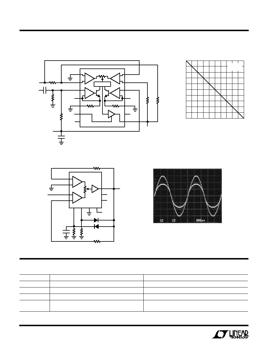
24
LT1251/LT1256
Linear Technology Corporation
1630 McCarthy Blvd., Milpitas, CA 95035-7417
(408) 432-1900
q
FAX
: (408) 434-0507
q
TELEX
: 499-3977
LT/GP 0896 REV A 5K ∑ PRINTED IN USA
©
LINEAR TECHNOLOGY CORPORATION 1994
TYPICAL APPLICATIO
N
S
U
4-Quadrant Multiplier as a Double-Sideband Suppressed-Carrier Modulator
Modulation Gain vs Control Voltage
≠
+
≠
+
1MHz
CARRIER
MODULATION
10k
10k*
R
F2
1.5k
V
OUT
R
F1
1.5k
I
C
V
+
V
≠
1251/56 TA04a
2
≠
+
≠
+
1
2
3
4
5
6
7
14
13
12
11
10
9
8
CONTROL
LT1256
1
C
FS
5k
5k
I
FS
0.1
µ
F
0.1
µ
F
*TRIM FOR SYMMETRY
2.5VDC
INPUT
R
G1
1.5k
CONTROL VOLTAGE, PIN 3 (V)
0
GAIN (V/
V)
1.0
0.8
0.6
0.4
0.2
0
≠0.2
≠0.4
≠0.6
≠0.8
≠1.0
2.0
1251/56 TA04b
0.5
1.0
1.5
2.5
V
S
= ±5V
V
FS
= 2.5V
1.5k
1.5k
1N914
1N914
1k
5k
V
IN
1251/56 TA10a
2
8
200pF
2.5VDC
INPUT
14
13
12
10
5
3
1
V
OUT
V
C
R
C
R
FS
V
FS
LT1256
≠
+
≠
+
2
1
9
7
V
+
V
≠
Soft Clipper
V
FS
= 2.5V
V
S
=
±
5V
f = 1kHz
1251/56 TA10b
V
IN
V
OUT
PART NUMBER
DESCRIPTION
COMMENTS
LT1228
100MHz Current Feedback Amplifier with DC Gain Control
Includes a 75MHz Transconductance Amplifier
LT1252
Low Cost Video Amplifier
100MHz Bandwidth
LT1253/LT1254
Low Cost Dual and Quad Video Amplifiers
90 MHz Bandwidth
LT1259/LT1260
Low Cost Dual and Triple 130MHz Current Feedback
Makes Fast Video MUX
Amplifiers with Shutdown
RELATED PARTS