 | –≠–ª–µ–∫—Ç—Ä–æ–Ω–Ω—ã–π –∫–æ–º–ø–æ–Ω–µ–Ω—Ç: LT1260CN | –°–∫–∞—á–∞—Ç—å:  PDF PDF  ZIP ZIP |
1
LT1259/LT1260
Low Cost Dual and Triple
130MHz Current Feedback
Amplifiers with Shutdown
Square Wave Response
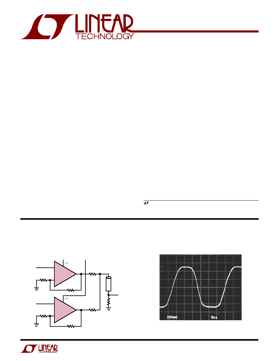
2-Input Video MUX Cable Driver
CABLE OUTPUT
R
L
= 150
f = 30MHz
LT1259/50 ∑ TA02
The LT
Æ
1259 contains two independent 130MHz current
feedback amplifiers, each with a shutdown pin. These
amplifiers are designed for excellent linearity while driving
cables and other low impedance loads. The LT1260 is a
triple version especially suited to RGB video applications.
These amplifiers operate on all supplies from single 5V to
±
15V and draw only 5mA per amplifier when active.
When shut down, the LT1259/LT1260 amplifiers draw
zero supply current and their outputs become high
impedance. Only two LT1260s are required to make a
complete 2-input RGB MUX and cable driver. These
amplifiers turn on in only 100ns and turn off in 40ns,
making them ideal in spread spectrum and portable
equipment applications.
The LT1259/LT1260 amplifiers are manufactured on
Linear Technology's proprietary complementary bipolar
process.
s
90MHz Bandwidth on
±
5V
s
0.1dB Gain Flatness > 30MHz
s
Completely Off in Shutdown, 0
µ
A Supply Current
s
High Slew Rate: 1600V/
µ
s
s
Wide Supply Range:
±
2V(4V) to
±
15V(30V)
s
60mA Output Current
s
Low Supply Current: 5mA/Amplifier
s
Differential Gain: 0.016%
s
Differential Phase: 0.075
∞
s
Fast Turn-On Time: 100ns
s
Fast Turn-Off Time: 40ns
s
14-Pin and 16-Pin Narrow SO Packages
s
RGB Cable Drivers
s
Spread Spectrum Amplifiers
s
MUX Amplifiers
s
Composite Video Cable Drivers
s
Portable Equipment
, LTC and LT are registered trademarks of Linear Technology Corporation.
≠
+
1/2 LT1259
R
G
1.6k
R
F
1.6k
A
EN A
V
IN A
≠
+
1/2 LT1259
R
G
1.6k
R
F
1.6k
EN B
V
IN B
B
CHANNEL
SELECT
75
75
75
V
OUT
75
CABLE
LT1259/60 ∑ TA01
FEATURES
DESCRIPTIO
U
APPLICATIO S
U
TYPICAL APPLICATIO
U
2
LT1259/LT1260
Supply Voltage .....................................................
±
18V
Input Current .....................................................
±
15mA
Output Short-Circuit Duration (Note 1) ......... Continuous
Specified Temperature Range (Note 2) ....... 0
∞
C to 70
∞
C
Operating Temperature Range ............... ≠ 40
∞
C to 85
∞
C
Storage Temperature Range ................ ≠ 65
∞
C to 150
∞
C
Junction Temperature (Note 4) ............................ 150
∞
C
Lead Temperature (Soldering, 10 sec).................. 300
∞
C
ORDER PART
NUMBER
ORDER PART
NUMBER
LT1259CN
LT1259CS
LT1259IN
LT1259IS
LT1260CN
LT1260CS
LT1260IN
LT1260IS
SYMBOL
PARAMETER
CONDITIONS
MIN
TYP
MAX
UNITS
V
OS
Input Offset Voltage
T
A
= 25
∞
C
2
12
mV
q
16
mV
Input Offset Voltage Drift
q
30
µ
V/
∞
C
I
IN
+
Noninverting Input Current
T
A
= 25
∞
C
0.5
3
µ
A
q
6
µ
A
I
IN
≠
Inverting Input Current
T
A
= 25
∞
C
20
90
µ
A
q
120
µ
A
e
n
Input Noise Voltage Density
f = 1kHz, R
F
= 1k, R
G
= 10
, R
S
= 0
3.6
nV/
Hz
+ i
n
Noninverting Input Noise Current Density
f = 1kHz
1.3
pA/
Hz
≠ i
n
Inverting Input Noise Current Density
f = 1kHz
45
pA/
Hz
R
IN
Input Resistance
V
IN
=
±
13V, V
S
=
±
15V
q
2
17
M
V
IN
=
±
3V, V
S
=
±
5V
q
2
25
M
C
IN
Input Capacitance
Enabled
2
pF
Disabled
4
pF
C
OUT
Output Capacitance
Disabled
4.4
pF
V
IN
Input Voltage Range
V
S
=
±
15V, T
A
= 25
∞
C
±
13
±
13.5
V
q
±
12
V
V
S
=
±
5V, T
A
= 25
∞
C
±
3
±
3.5
V
q
±
2
V
0
∞
C
T
A
70
∞
C, each amplifier V
CM
= 0V,
±
5V
V
S
±
15V, EN pins = 0V, pulse tested, unless otherwise noted.
Consult factory for Military grade parts.
T
JMAX
= 150
∞
C,
JA
= 70
∞
C/W (N)
T
JMAX
= 150
∞
C,
JA
= 100
∞
C/W (S)
1
2
3
4
5
6
7
8
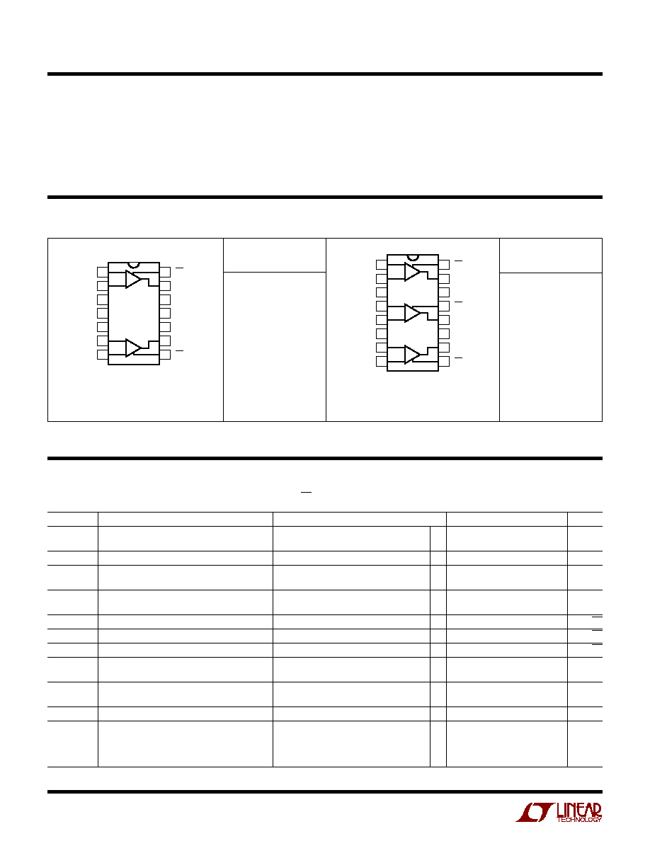
TOP VIEW
N PACKAGE
16-LEAD PLASTIC DIP
16
15
14
13
12
11
10
9
≠IN R
+IN R
GND
≠IN G
+IN G
GND
+IN B
≠IN B
EN R
OUT R
V
+
EN G
OUT G
V
≠
OUT B
EN B
R
S PACKAGE
16-LEAD PLASTIC SOIC
G
B
T
JMAX
= 150
∞
C,
JA
= 70
∞
C/W (N)
T
JMAX
= 150
∞
C,
JA
= 110
∞
C/W (S)
1
2
3
4
5
6
7
TOP VIEW
S PACKAGE
14-LEAD PLASTIC SOIC
N PACKAGE
14-LEAD PLASTIC DIP
14
13
12
11
10
9
8
≠IN A
+IN A
GND
GND
GND
+IN B
≠IN B
EN A
OUT A
V
+
GND
V
≠
OUT B
EN B
A
B
ABSOLUTE AXI U RATI GS
W
W
W
U
PACKAGE/ORDER I FOR ATIO
U
U
W
ELECTRICAL CHARACTERISTICS
3
LT1259/LT1260
ELECTRICAL C
C
HARA TERISTICS
SYMBOL
PARAMETER
CONDITIONS
MIN
TYP
MAX
UNITS
V
OUT
Maximum Output Voltage Swing
V
S
=
±
15V, R
L
= 1k
q
±
12.0
±
14.0
V
V
S
=
±
5V, R
L
= 150
, T
A
= 25
∞
C
±
3.0
±
3.7
V
q
±
2.5
V
CMRR
Common-Mode Rejection Ratio
V
S
=
±
15V, V
CM
=
±
13V, T
A
= 25
∞
C
55
69
dB
V
S
=
±
15V, V
CM
=
±
12V
q
55
dB
V
S
=
±
5V, V
CM
=
±
3V, T
A
= 25
∞
C
52
63
dB
V
S
=
±
5V, V
CM
=
±
2V
q
52
dB
Inverting Input Current
V
S
=
±
15V, V
CM
=
±
13V, T
A
= 25
∞
C
3.5
10
µ
A/V
Common-Mode Rejection
V
S
=
±
15V, V
CM
=
±
12V
q
10
µ
A/V
V
S
=
±
5V, V
CM
=
±
3V, T
A
= 25
∞
C
4.5
15
µ
A/V
V
S
=
±
5V, V
CM
=
±
2V
q
15
µ
A/V
PSRR
Power Supply Rejection Ratio
V
S
=
±
2V to
±
15V, EN Pins at V
≠
, T
A
= 25
∞
C
60
80
dB
V
S
=
±
3V to
±
15V, EN Pins at V
≠
q
60
dB
Noninverting Input Current
V
S
=
±
3V to
±
15V, EN Pins at V
≠
, T
A
= 25
∞
C
15
65
nA/V
Power Supply Rejection
V
S
=
±
3V to
±
15V, EN Pins at V
≠
q
75
nA/V
Inverting Input Current
V
S
=
±
2V to
±
15V, EN Pins at V
≠
, T
A
= 25
∞
C
0.1
5
µ
A/V
Power Supply Rejection
V
S
=
±
3V to
±
15V, EN Pins at V
≠
q
5
µ
A/V
A
V
Large-Signal Voltage Gain
V
S
=
±
15V, V
OUT
=
±
10V, R
L
= 1k
q
57
72
dB
V
S
=
±
5V, V
OUT
=
±
2V, R
L
= 150
q
57
69
dB
R
OL
Transresistance,
V
OUT
/
I
IN
≠
V
S
=
±
15V, V
OUT
=
±
10V, R
L
= 1k
q
120
300
k
V
S
=
±
5V, V
OUT
=
±
2V, R
L
= 150
q
100
200
k
I
OUT
Maximum Output Current
R
L
= 0
, T
A
= 25
∞
C
30
60
mA
I
S
Supply Current per Amplifier
V
S
=
±
15V, V
OUT
= 0V, T
A
= 25
∞
C
5.0
7.5
mA
(Note 5)
q
7.9
mA
V
S
=
±
5V, V
OUT
= 0V, T
A
= 25
∞
C
4.5
6.7
mA
Disable Supply Current per Amplifier
V
S
=
±
15V, EN Pin Voltage = 14.5V, R
L
= 150
q
3
16.7
µ
A
V
S
=
±
15V, Sink 1
µ
A From EN Pin
q
1
2.7
µ
A
Enable Pin Current
V
S
=
±
15V, EN Pin Voltage = 0V, T
A
= 25
∞
C
60
200
µ
A
q
300
µ
A
SR
Slew Rate (Note 6)
T
A
= 25
∞
C
900
1600
V/
µ
s
t
ON
Turn-On Delay Time (Note 7)
A
V
= 10, T
A
= 25
∞
C
100
400
ns
t
OFF
Turn-Off Delay Time (Note 7)
A
V
= 10, T
A
= 25
∞
C
40
150
ns
t
r
, t
f
Small-Signal Rise and Fall Time
V
S
=
±
12V, R
F
= R
G
= 1.5k, R
L
= 150
4.2
ns
Propagation Delay
V
S
=
±
12V, R
F
= R
G
= 1.5k, R
L
= 150
4.7
ns
Small-Signal Overshoot
V
S
=
±
12V, R
F
= R
G
= 1.5k, R
L
= 150
5
%
t
S
Settling Time
0.1%, V
OUT
= 10V, R
F
= R
G
= 1.5k, R
L
= 1k
75
ns
Differential Gain (Note 8)
V
S
=
±
12V, R
F
= R
G
= 1.5k, R
L
= 150
0.016
%
Differential Phase (Note 8)
V
S
=
±
12V, R
F
= R
G
= 1.5k, R
L
= 150
0.075
DEG
0
∞
C
T
A
70
∞
C, each amplifier V
CM
= 0V,
±
5V
V
S
±
15V, EN pins = 0V, pulse tested, unless otherwise noted.
≠ 40
∞
C
T
A
85
∞
C, each amplifier V
CM
= 0V,
±
5V
V
S
±
15V, EN pins = 0V, pulse tested, unless otherwise noted.
SYMBOL
PARAMETER
CONDITIONS
MIN
TYP
MAX
UNITS
V
OS
Input Offset Voltage
q
18
mV
I
IN
+
Noninverting Input Current
q
7
µ
A
I
IN
≠
Inverting Input Current
q
130
µ
A
R
IN
Input Resistance
V
IN
=
±
3V, V
S
=
±
5V
q
1
M
A
V
Large-Signal Gain
q
55
dB
I
S
Disable Supply Current per Amplifier
V
S
=
±
15V, EN Pin Voltage = 14.5V, R
L
= 150
q
19
µ
A
Enable Pin Current
V
S
=
±
15V, EN Pin Voltage = 0V
q
350
µ
A
4
LT1259/LT1260
The
q
denotes specifications which apply over the specified operating
temperature range.
Note 1: A heat sink may be required depending on the power supply
voltage and how many amplifiers have their outputs short circuited.
Note 2: Commercial grade parts are designed to operate over the
temperature range of ≠ 40
∞
C to 85
∞
C but are neither tested nor guaranteed
beyond 0
∞
C to 70
∞
C. Industrial grade parts specified and tested over
≠ 40
∞
C to 85
∞
C are available on special request. Consult factory.
Note 3: Ground pins are not internally connected. For best
performance, connect to ground.
Note 4: T
J
is calculated from the ambient temperature T
A
and the
power dissipation P
D
according to the following formulas:
LT1259CN/LT1259IN: T
J
= T
A
+ (P
D
∑ 70
∞
C/W)
LT1259CS/LT1259IS: T
J
= T
A
+ (P
D
∑ 110
∞
C/W)
LT1260CNLT1260IN/: T
J
= T
A
+ (P
D
∑ 70
∞
C/W)
LT1260CS/LT1260IS: T
J
= T
A
+ (P
D
∑ 100
∞
C/W)
Note 5: The supply current of the LT1259/LT1260 has a negative
temperature coefficient. See Typical Performance Characteristics.
Note 6: Slew rate is measured at
±
5V on a
±
10V output signal while
operating on
±
15V supplies with R
F
= 1k, R
G
= 110
and R
L
= 1k.
Note 7: Turn-on delay time is measured while operating on
±
5V
supplies with R
F
= 1k, R
G
= 110
and R
L
= 150
. The t
ON
is measured
from control input to appearance of 0.5V at the output, for V
IN
= 0.1V.
Likewise, turn-off delay time is measured from control input to
appearance of 0.5V on the output for V
IN
= 0.1V.
Note 8: Differential gain and phase are measured using a Tektronix
TSG120YC/NTSC signal generator and a Tektronix 1780R Video
Measurement Set. The resolution of this equipment is 0.1% and 0.1
∞
.
Six identical amplifier stages were cascaded giving an effective
resolution of 0.016% and 0.016
∞
.
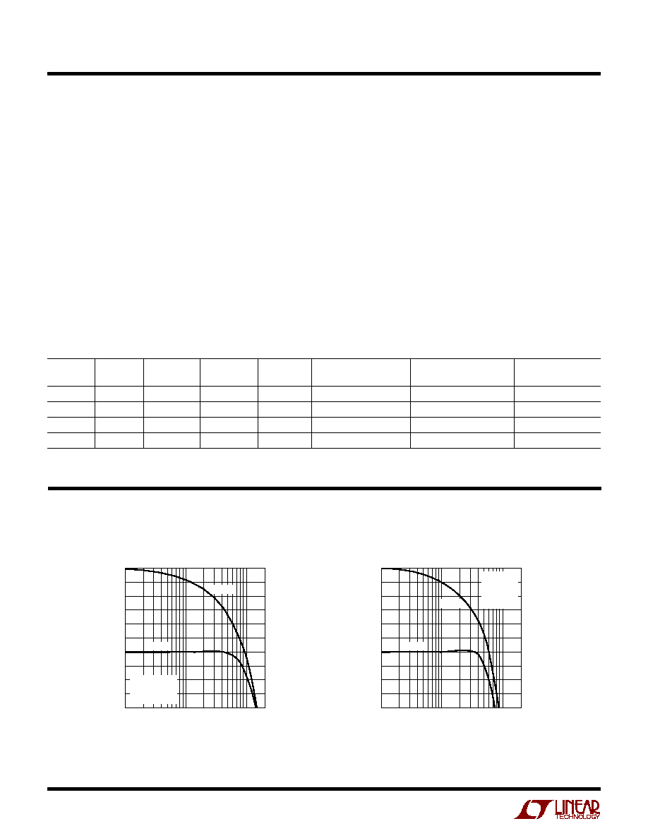
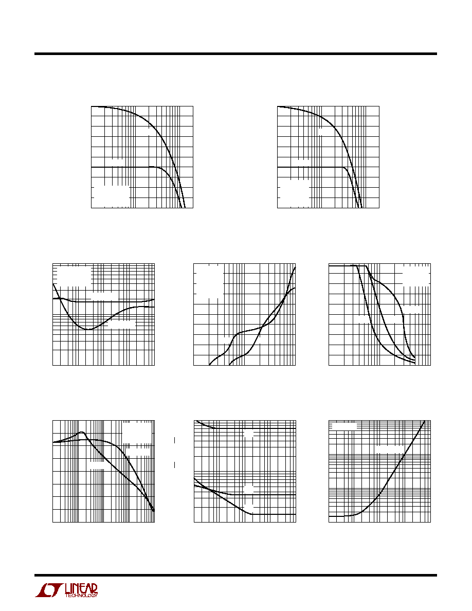
SMALL SIGNAL
SMALL SIGNAL
SMALL SIGNAL
V
S
(V)
A
V
R
L
(
)
R
F
(
)
R
G
(
)
≠ 3dB BW (MHz)
0.1dB BW (MHz)
PEAKING (dB)
±
12
2
150
1.5k
1.5k
130
53
0.1
±
5
2
150
1.1k
1.1k
93
40
0
±
12
10
150
1.1k
121
69
20
0.13
±
5
10
150
825
90.9
61
16
0
±
12V Frequency Response, A
V
= 2
FREQUENCY (MHz)
1
2
GAIN (dB)
4
6
8
10
10
100
LT1259/60 ∑ TPC01
3
5
7
9
11
12
≠200
≠160
≠120
≠80
≠40
≠180
≠140
≠100
≠60
0
PHASE (DEG)
PHASE
GAIN
V
S
= ±12V
R
L
= 150
R
F
= R
G
= 1.5k
≠20
FREQUENCY (MHz)
1
16
GAIN (dB)
18
20
22
24
10
100
LT1259/60 ∑ TPC01
17
19
21
23
25
26
≠200
≠160
≠120
≠80
≠40
≠180
≠140
≠100
≠60
0
PHASE (DEG)
PHASE
GAIN
V
S
= ±12V
R
L
= 150
R
F
= 1.1k
R
G
= 121
≠20
±
12V Frequency Response, A
V
= 10
ELECTRICAL CHARACTERISTICS
W
U
TYPICAL AC PERFOR A CE
TYPICAL PERFOR A CE CHARACTERISTICS
U
W
5
LT1259/LT1260
±
5V Frequency Response, A
V
= 2
FREQUENCY (MHz)
1
2
GAIN (dB)
4
6
8
10
10
100
LT1259/60 ∑ TPC03
3
5
7
9
11
12
≠200
≠160
≠120
≠80
≠40
≠180
≠140
≠100
≠60
0
PHASE (DEG)
PHASE
GAIN
V
S
= ±5V
R
L
= 150
R
F
= R
G
= 1.1k
≠20
FREQUENCY (MHz)
1
16
GAIN (dB)
18
20
22
24
10
100
LT1259/60 ∑ TPC04
17
19
21
23
25
26
≠200
≠160
≠120
≠80
≠40
≠180
≠140
≠100
≠60
0
PHASE (DEG)
PHASE
GAIN
V
S
= ±5V
R
L
= 150
R
F
= 825
R
G
= 90.9
≠20
Total Harmonic Distortion
vs Frequency
FREQUENCY (Hz)
10
0.001
TOTAL HARMONIC DISTORTION (%)
0.01
0.1
1k
100k
LT1259/60 ∑ TPC05
100
10k
V
S
= ±12V
R
L
= 400
R
F
= R
G
= 1.5k
V
O
= 6V
RMS
V
O
= 1V
RMS
2nd and 3rd Harmonic Distortion
vs Frequency
FREQUENCY (MHz)
1
≠70
DISTORTION (dBc)
≠60
≠50
≠40
≠30
10
100
LT12359/60 ∑ TPC06
≠20
2ND
3RD
V
S
= ±12V
V
O
= 2V
P-P
A
V
= 10dB
R
L
= 100
R
F
= 1.5k
Maximum Undistorted Output
vs Frequency
FREQUENCY (MHz)
1
0
OUTPUT VOLTAGE (V
P-P
)
5
10
15
20
10
100
LT12359/60 ∑ TPC07
25
V
S
= ±15V
R
L
= 1k
R
F
= 2k
A
V
= 1
A
V
= 2
A
V
= 10
Power Supply Rejection
vs Frequency
FREQUENCY (Hz)
20
POWER SUPPLY REJECTION (dB)
40
50
70
80
100k
1M
10M
LTC1259/60 ∑ TPC08
0
10k
60
30
10
100M
V
S
= ±15V
R
L
= 1OO
R
F
= R
G
= 1k
POSITIVE
NEGATIVE
Spot Noise Voltage and Current
vs Frequency
Output Impedance vs Frequency
±
5V Frequency Response, A
V
= 10
FREQUENCY (Hz)
10k
OUTPUT IMPEDANCE (
)
1
100
1M
100M
LT1259/60 ∑ TPC10
0.1
10
100k
10M
V
S
= ±15V
R
F
= R
G
= 2k
FREQUENCY (Hz)
10
1
SPOT NOISE (nV/
Hz OR pA/
Hz)
10
100
1k
100k
LT1259/60 ∑ TPC09
100
10k
≠i
n
e
n
+i
n
TYPICAL PERFOR A CE CHARACTERISTICS
U
W