 | –≠–ª–µ–∫—Ç—Ä–æ–Ω–Ω—ã–π –∫–æ–º–ø–æ–Ω–µ–Ω—Ç: LT1268 | –°–∫–∞—á–∞—Ç—å:  PDF PDF  ZIP ZIP |
1
LT1268B/LT1268
7.5A, 150kHz
Switching Regulators
S
FEATURE
D
U
ESCRIPTIO
s
Wide Input Voltage Range: 3.5V to 30V
s
Low Quiescent Current: 7mA
s
Internal 7.5A Switch
s
Very Few External Parts Required
s
Self-Protected Against Overloads
s
Available in Standard and Surface Mount
5-Pin Packages
s
Can Be Externally Synchronized
(See LT1072 Data Sheet)
The LT1268B and LT1268 are monolithic high power
switching regulators. Identical to the popular LT1070,
except for switching frequency (150kHz) and higher
switch current, they can be operated in all standard
switching configurations including buck, boost, flyback,
and inverting. A high current, high efficiency switch is
included on the die along with all oscillator, control, and
protection circuitry. Integration of all functions allows
the LT1268 to be built in standard 5-pin power packages.
This makes it extremely easy to use and provides "bust
proof" operations similar to that obtained with 3-pin
linear regulators.
The LT1268 operate with supply voltages from 3.5V to
30V and draw only 7mA quiescent current. By utilizing
current mode switching techniques, it provides excellent
AC and DC load and line regulation.
The LT1268 use an adaptive anti-sat switch drive to allow
very wide ranging load currents with no loss in efficiency.
An externally activated shutdown mode reduces total
supply current to 100
µ
A typical for standby operation.
USER NOTE:
This data sheet is only intended to provide specifications, graphs, and a general functional
description of the LT1268B/LT1268. Application circuits are included to show the capability of the
LT1268B/LT1268. A complete design manual (AN19) should be obtained to assist in developing new
designs. This manual contains a comprehensive discussion of both the LT1070 and the external
components used with it, as well as complete formulas for calculating the values of these
components. The manual can also be used for the LT1268B/LT1268 factoring in the higher switch
current rating and higher operating frequency.
U
A
O
PPLICATI
TYPICAL
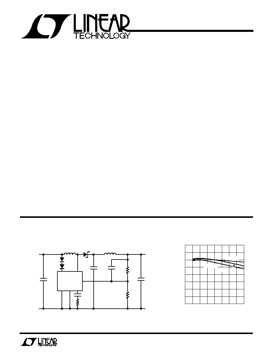
Boost Regulator with 5.3V
±
1% Output
LOAD CURRENT (A)
0
EFFICIENCY (%)
80
90
4
LT1268 ∑ TA02
70
60
1
2
3
100
V
IN
= 5.3V
V
IN
= 4.7V
V
IN
= 5V
Efficiency of 5.3V Boost Converter
V
IN
V
SW
LT1268B
L1
8
µ
H, 5A*
D1
MBR1035
D2, D3
1N4001
C2
0.068
C3
390
µ
F
16V
R1
4.043k
0.1%
R2
1.24k
0.1%
R3
220
FB
GND
V
C
CASE
L2
2
µ
H, 5A**
C1
220
µ
F
16V
+
+
C4
390
µ
F
16V
V
OUT
5.3V ±1%
3.75A
V
IN
4.7V TO
5.3V
LT1268 ∑ TA01
COILTRONICS CTX8-5-52
COILTRONICS CTX2-5-52
OPTIONAL. D2 AND D3 ARE USED TO INCREASE
UNDERVOLTAGE LOCKOUT FROM 2.7V TO
4V.
*
**
+
C5
0.02
U
S
A
O
PPLICATI
s
High Efficiency Boost Converter
s
PC Power Supply with Multiple Outputs
s
Battery Upconverter
s
Negative-to-Positive Converter
2
LT1268B/LT1268
A
U
G
W
A
W
U
W
A
R
BSOLUTE
XI
TI
S
Supply Voltage ....................................................... 30V
Switch Output Voltage ............................................ 60V
Feedback Pin Voltage (Transient, 1ms) ................
±
15V
Operating Junction Temperature Range
Operating ............................................... 0
∞
C to 125
∞
C
Short-Circuit ......................................... 0
∞
C to 140
∞
C
Storage Temperature Range ................. ≠ 65
∞
C to 150
∞
C
Lead Temperature (Soldering, 10 sec).................. 300
∞
C
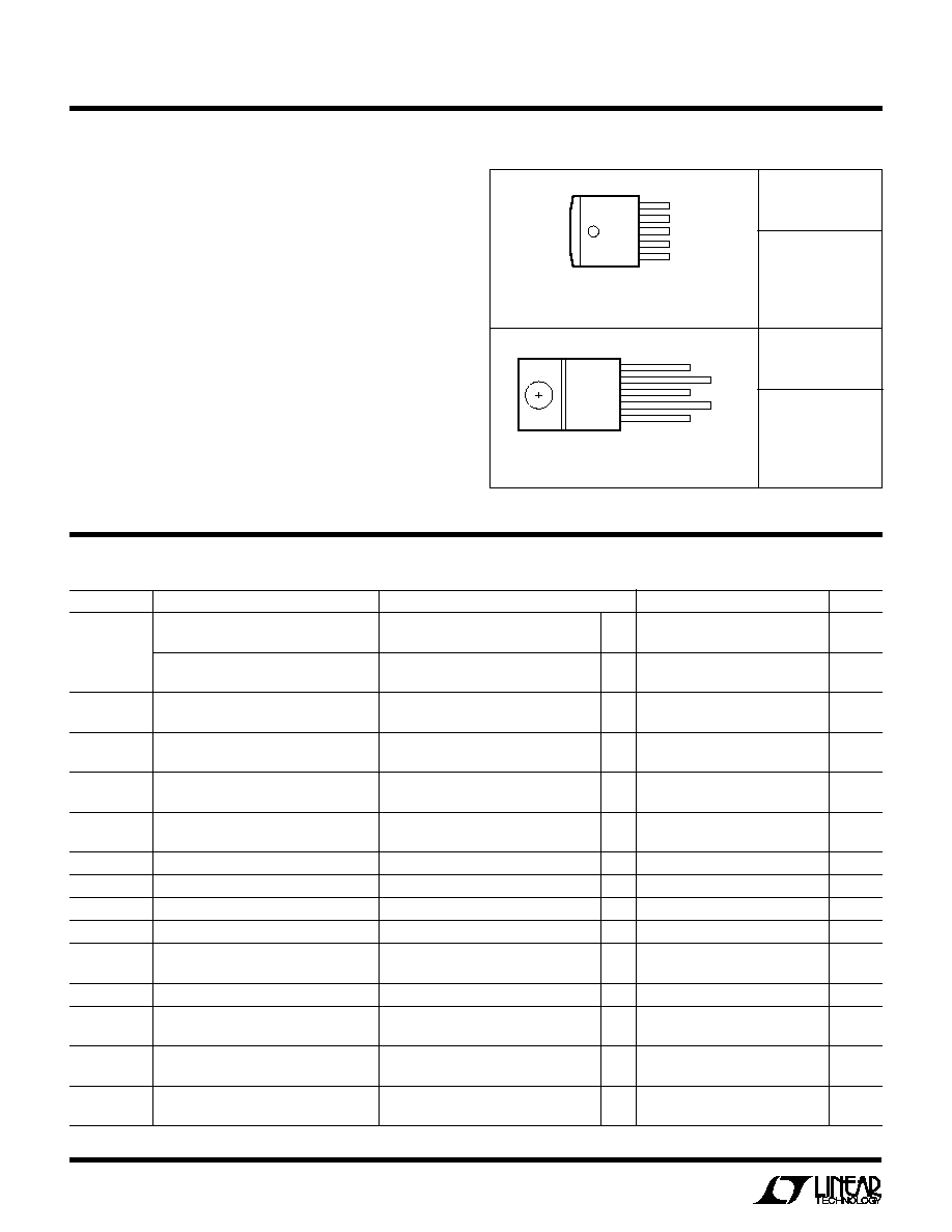
ORDER PART
NUMBER
W
U
U
PACKAGE/ORDER I FOR ATIO
ORDER PART
NUMBER
T
JMAX
= 125
∞
C,
JC
= 2
∞
C/W,
JA
= 50
∞
C/W
LT1268CT
LT1268BCT
T
JMAX
= 125
∞
C,
JC
= 2
∞
C/ W,
JA
= See Notes 5 and 6
Q PACKAGE
5-LEAD DD
FRONT VIEW
V
IN
V
SW
GND
FB
V
C
5
4
3
2
1
LT1268CQ
LT1268BCQ
T PACKAGE
5-LEAD TO-220
V
IN
V
SW
GND
FB
V
C
FRONT VIEW
5
4
3
2
1
SYMBOL
PARAMETER
CONDITIONS
MIN
TYP
MAX
UNITS
V
REF
Reference Voltage Measured at
LT1268B
1.235
1.244
1.253
V
Feedback Pin (Note 4)
q
1.224
1.244
1.264
V
Reference Voltage
LT1268
1.224
1.244
1.264
V
q
1.214
1.244
1.274
V
I
B
Feedback Input Current
V
FB
= V
REF
350
750
nA
q
1100
nA
g
m
Error Amplifier Transconductance
I
C
=
±
25
µ
A
3000
4400
6000
µ
mho
q
2400
7000
µ
mho
Error Amplifier Source or Sink Current
V
C
= 1.5V
150
200
350
µ
A
q
120
400
µ
A
Error Amplifier Clamp Voltage
Hi Clamp, V
FB
= 1V
1.80
2.30
V
Lo Clamp, V
FB
= 1.5V
0.25
0.38
0.52
V
Reference Voltage Line Regulation
3V
V
IN
V
MAX
, V
C
= 0.8V
q
0.03
%/V
A
V
Error Amplifier Voltage Gain
0.9V
V
C
1.4V
500
800
V/V
Minimum Input Voltage
q
2.8
3.0
V
I
Q
Supply Current
3V
V
IN
V
MAX
, V
C
= 0.6V
7
10
mA
Control Pin Threshold
Duty Cycle = 0
0.7
0.9
1.08
V
q
0.5
1.25
V
BV
Output Switch Breakdown Voltage
3V
V
IN
V
MAX
, I
SW
= 1.5mA
q
60
75
V
V
SAT
Output Switch-ON Resistance
T
J
100
∞
C
0.12
0.18
(Note 1, 3)
T
J
125
∞
C
0.22
Control Voltage to Switch
12
A/V
Current Transconductance
I
LIM
Switch Current Limit (Note 3, 6)
Duty Cycle = 50%, T
J
100
∞
C
q
7.50
15
A
Duty Cycle = 65%, T
J
100
∞
C
q
6.50
14
A
V
IN
= 15V, V
C
= 0.5V, V
FB
= V
REF
, switch pin open, unless otherwise noted.
ELECTRICAL C
C
HARA TERISTICS
Consult factory for Industrial and Military parts
3
LT1268B/LT1268
Information furnished by Linear Technology Corporation is believed to be accurate and reliable. However,
no responsibility is assumed for its use. Linear Technology Corporation makes no representation that
the interconnection of its circuits as described herein will not infringe on existing patent rights.
SYMBOL
PARAMETER
CONDITIONS
MIN
TYP
MAX
UNITS
I
IN
Supply Current Increase
25
45
mA/A
I
SW
During Switch-ON Time
f
Switching Frequency
120
150
180
kHz
q
120
180
kHz
DC
MAX
Maximum Switch Duty Cycle
65
85
92
%
Shutdown Mode Supply Current
3V
V
IN
V
MAX
, V
C
= 0.05V
100
500
µ
A
Shutdown Mode Threshold Voltage
3V
V
IN
V
MAX
100
150
250
mV
q
50
300
mV
V
IN
= 15V, V
C
= 0.5V, V
FB
= V
REF
, switch pin open, unless otherwise noted.
ELECTRICAL C
C
HARA TERISTICS
The
q
denotes specifications which apply over the full operating
temperature range.
Note 1: Measured with V
C
in hi clamp, V
FB
= 0.8V.
Note 2: For duty cycles (DC) between 50% and 65%, minimum guaranteed
switch current is given by I
LIM
= 6.25 (1.7 ≠ DC).
Note 3: Minimum current limit is reduced by 0.5A at 125
∞
C. 100
∞
C test
limits are guaranteed by correlation to 125
∞
C tests.
Note 4: LT1268B reference voltage is specified at
±
9mV to guarantee
±
1%
output voltage accuracy when 0.1% external resistors are used to set
output voltage. To maintain output accuracy under load, load current
should be taken from the case and the ground pin should be connected
separately to output ground. See AN19 for details.
Note 5: The Q package is intended for surface mount without a separate
heat sink. See graph for thermal resistance as a function of the mounting
area. This curve assumes no other heat dissipators adjacent to package.
Note 6: Maximum switch current may be limited by package power
dissipation, especially for the surface mount (Q) package. This package
has a thermal resistance of 20
∞
C/W to 50
∞
C/W (see graph). The following
formula will allow an estimate of maximum continuous switch current as a
function of power loss and duty cycle. See AN19 for more details.
I
MAX
=
P
R
SW
◊
DC
P = Power dissipation due to switch current
R
SW
= Switch-ON resistance
0.15
DC = Switch duty cycle
In a typical application where thermal resistance is 30
∞
C/W, maximum
power might be limited to 2W and power allocated to switch loss is 1.5W.
For a duty cycle of 40%, this yields
I
MAX
=
= 5A
1.5
0.15
◊
0.4
Obviously, a combination of high thermal resistance and high duty cycle
may restrict switch current to a value well below the 7.5A electrical limit.
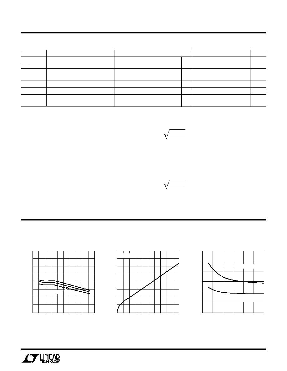
TYPICAL PERFOR A CE CHARACTERISTICS
W U
DUTY CYCLE (%)
0
SWITCH CURRENT (A)
18
24
80
LT1268 ∑ TPC01
12
6
0
20
40
60
100
70
10
30
50
90
≠55∞C
125∞C
25∞C
Switch Current Limit vs Duty Cycle
TOP SURFACE COPPER AREA (cm
2
)
0
0
(∞C/
W)
10
20
30
40
60
5
10
15
20
LT1268 ∑ 603
25
30
50
SINGLE-SIDED BOARD, 1oz COPPER
DOUBLE-SIDED BOARD, 1oz COPPER
BOTTOM COPPER AREA >100cm
2
SWITCH CURRENT (A)
0
SWITCH SATURATION VOLTAGE (V)
1.2
1.6
8
LT1268 ∑ TPC02
0.8
0.4
1.0
1.4
0.6
0.2
0
2
4
6
10
7
1
3
5
9
T
J
= 25∞C
Switch Saturation Voltage
Q Package Thermal Resistance
4
LT1268B/LT1268
Linear Technology Corporation
1630 McCarthy Blvd., Milpitas, CA 95035-7487
(408) 432-1900
q
FAX
: (408) 434-0507
q
TELEX
: 499-3977
©
LINEAR TECHNOLOGY CORPORATION 1994
1268fs, sn1268 LT/GP 0194 10K REV 0 ∑ PRINTED IN THE USA
U
A
O
PPLICATI
TYPICAL
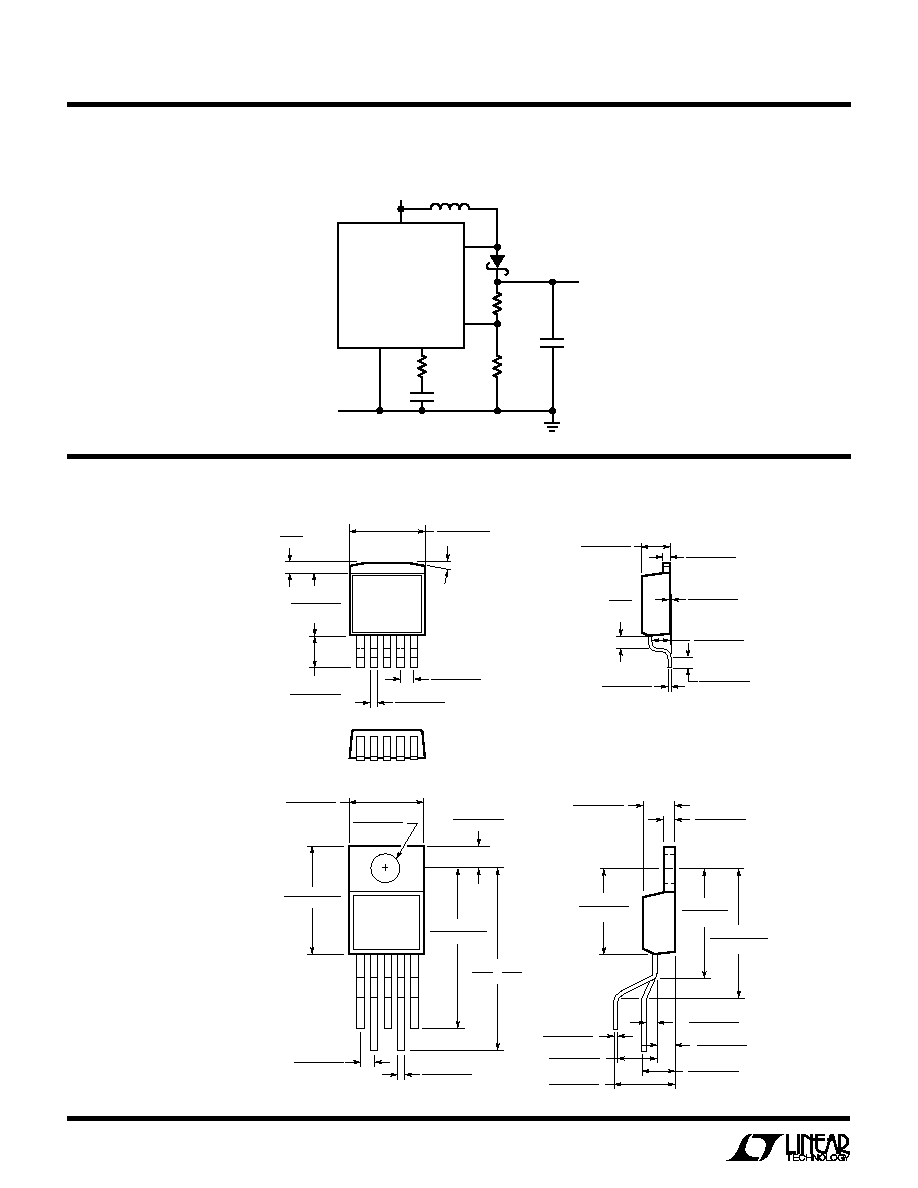
Boost Converter (5V TO 12V)
Q Package
5-Lead DD
T Package
5-Lead TO-220
V
IN
20
µ
H
5V
V
SW
LT1268CT
LT1268 ∑ TA03
FB
1k
1.24k
10.7k
12V, 1.5A
MBR1020
1
µ
F
1000
µ
F
25V
V
C
GND
+
+
PACKAGE DESCRIPTIO
U
Dimensions in inches (millimeters) unless otherwise noted.
0.022 ± 0.005
(0.559 ± 0.127)
0.105 ± 0.008
(2.667 ± 0.203)
0.004
+0.008
≠0.004
(
)
0.102
+0.203
≠0.102
0.050 ± 0.012
(1.270 ± 0.305)
0.059
(1.499)
TYP
0.050 ± 0.008
(1.270 ± 0.203)
0.175 ± 0.008
(4.445 ± 0.203)
0.060
(1.524)
0.401 ± 0.015
(10.185 ± 0.381)
15∞ TYP
0.032 ± 0.008
(0.813 ± 0.203)
0.331
+0.012
≠0.020
(
)
8.407
+0.305
≠0.508
0.143
+0.012
≠0.020
(
)
3.632
+0.305
≠0.508
0.067 ± 0.010
(1.702 ± 0.254)
0.028 ≠ 0.035
(0.711 ≠ 0.889)
0.057 ≠ 0.077
(1.448 ≠ 1.956)
0.139 ≠ 0.153
(3.531 ≠ 3.886)
DIA
0.079 ≠ 0.135
(2.007 ≠ 3.429)
0.380 ≠ 0.420
(9.652 ≠ 10.668)
0.560 ≠ 0.650
(14.224 ≠ 16.510)
0.866 ≠ 0.913
(21.996 ≠ 23.190)
0.970 ≠ 1.050
(24.64 ≠ 26.67)
0.304 ≠ 0.380
(7.722 ≠ 9.652)
0.700 ≠ 0.728
(17.780 ≠ 18.491)
0.035 ≠ 0.055
(0.889 ≠ 1.397)
0.169 ≠ 0.185
(4.293 ≠ 4.699)
0.079 ≠ 0.115
(2.007 ≠ 2.921)
0.149 ≠ 0.230
(3.785 ≠ 5.842)
0.620 ± 0.020
(15.75 ± 0.508)
0.460 ≠ 0.500
(11.68 ≠ 12.70)
0.210 ≠ 0.240
(5.334 ≠ 6.096)
0.055 ≠ 0.090
(1.397 ≠ 2.286)
0.015 ≠ 0.025
(0.381 ≠ 0.635)